EP0075924A2 - Dispositif capteur d'image à l'état solide présentant une grande résolution et une grande sensitivité - Google Patents
Dispositif capteur d'image à l'état solide présentant une grande résolution et une grande sensitivité Download PDFInfo
- Publication number
- EP0075924A2 EP0075924A2 EP82108964A EP82108964A EP0075924A2 EP 0075924 A2 EP0075924 A2 EP 0075924A2 EP 82108964 A EP82108964 A EP 82108964A EP 82108964 A EP82108964 A EP 82108964A EP 0075924 A2 EP0075924 A2 EP 0075924A2
- Authority
- EP
- European Patent Office
- Prior art keywords
- image pick
- state image
- solid state
- semiconductor layer
- semiconductor
- Prior art date
- Legal status (The legal status is an assumption and is not a legal conclusion. Google has not performed a legal analysis and makes no representation as to the accuracy of the status listed.)
- Withdrawn
Links
- 239000007787 solid Substances 0.000 title claims abstract description 23
- 230000035945 sensitivity Effects 0.000 title abstract description 12
- 239000004065 semiconductor Substances 0.000 claims abstract description 48
- 239000000758 substrate Substances 0.000 claims abstract description 20
- 239000012212 insulator Substances 0.000 claims abstract description 15
- 230000004888 barrier function Effects 0.000 claims abstract description 8
- 108091006146 Channels Proteins 0.000 description 18
- 239000000969 carrier Substances 0.000 description 17
- 238000000034 method Methods 0.000 description 10
- 238000004519 manufacturing process Methods 0.000 description 6
- 229910052581 Si3N4 Inorganic materials 0.000 description 5
- HQVNEWCFYHHQES-UHFFFAOYSA-N silicon nitride Chemical compound N12[Si]34N5[Si]62N3[Si]51N64 HQVNEWCFYHHQES-UHFFFAOYSA-N 0.000 description 5
- 230000003247 decreasing effect Effects 0.000 description 3
- 238000006243 chemical reaction Methods 0.000 description 2
- 238000005229 chemical vapour deposition Methods 0.000 description 2
- 230000006866 deterioration Effects 0.000 description 2
- 150000002500 ions Chemical class 0.000 description 2
- SYQQWGGBOQFINV-FBWHQHKGSA-N 4-[2-[(2s,8s,9s,10r,13r,14s,17r)-10,13-dimethyl-17-[(2r)-6-methylheptan-2-yl]-3-oxo-1,2,6,7,8,9,11,12,14,15,16,17-dodecahydrocyclopenta[a]phenanthren-2-yl]ethoxy]-4-oxobutanoic acid Chemical compound C1CC2=CC(=O)[C@H](CCOC(=O)CCC(O)=O)C[C@]2(C)[C@@H]2[C@@H]1[C@@H]1CC[C@H]([C@H](C)CCCC(C)C)[C@@]1(C)CC2 SYQQWGGBOQFINV-FBWHQHKGSA-N 0.000 description 1
- ZOXJGFHDIHLPTG-UHFFFAOYSA-N Boron Chemical compound [B] ZOXJGFHDIHLPTG-UHFFFAOYSA-N 0.000 description 1
- 108010075750 P-Type Calcium Channels Proteins 0.000 description 1
- 206010034972 Photosensitivity reaction Diseases 0.000 description 1
- VYPSYNLAJGMNEJ-UHFFFAOYSA-N Silicium dioxide Chemical compound O=[Si]=O VYPSYNLAJGMNEJ-UHFFFAOYSA-N 0.000 description 1
- 238000000137 annealing Methods 0.000 description 1
- 239000012298 atmosphere Substances 0.000 description 1
- QVGXLLKOCUKJST-UHFFFAOYSA-N atomic oxygen Chemical compound [O] QVGXLLKOCUKJST-UHFFFAOYSA-N 0.000 description 1
- 230000015572 biosynthetic process Effects 0.000 description 1
- 229910052796 boron Inorganic materials 0.000 description 1
- 238000009792 diffusion process Methods 0.000 description 1
- BHEPBYXIRTUNPN-UHFFFAOYSA-N hydridophosphorus(.) (triplet) Chemical compound [PH] BHEPBYXIRTUNPN-UHFFFAOYSA-N 0.000 description 1
- 239000012535 impurity Substances 0.000 description 1
- 239000012299 nitrogen atmosphere Substances 0.000 description 1
- 230000003647 oxidation Effects 0.000 description 1
- 238000007254 oxidation reaction Methods 0.000 description 1
- 239000001301 oxygen Substances 0.000 description 1
- 229910052760 oxygen Inorganic materials 0.000 description 1
- 230000036211 photosensitivity Effects 0.000 description 1
- 238000001020 plasma etching Methods 0.000 description 1
- 238000005036 potential barrier Methods 0.000 description 1
- 238000005215 recombination Methods 0.000 description 1
- 230000006798 recombination Effects 0.000 description 1
- 229910052814 silicon oxide Inorganic materials 0.000 description 1
Images
Classifications
-
- H—ELECTRICITY
- H10—SEMICONDUCTOR DEVICES; ELECTRIC SOLID-STATE DEVICES NOT OTHERWISE PROVIDED FOR
- H10F—INORGANIC SEMICONDUCTOR DEVICES SENSITIVE TO INFRARED RADIATION, LIGHT, ELECTROMAGNETIC RADIATION OF SHORTER WAVELENGTH OR CORPUSCULAR RADIATION
- H10F39/00—Integrated devices, or assemblies of multiple devices, comprising at least one element covered by group H10F30/00, e.g. radiation detectors comprising photodiode arrays
- H10F39/10—Integrated devices
- H10F39/12—Image sensors
- H10F39/15—Charge-coupled device [CCD] image sensors
- H10F39/152—One-dimensional array CCD image sensors
-
- H—ELECTRICITY
- H10—SEMICONDUCTOR DEVICES; ELECTRIC SOLID-STATE DEVICES NOT OTHERWISE PROVIDED FOR
- H10F—INORGANIC SEMICONDUCTOR DEVICES SENSITIVE TO INFRARED RADIATION, LIGHT, ELECTROMAGNETIC RADIATION OF SHORTER WAVELENGTH OR CORPUSCULAR RADIATION
- H10F39/00—Integrated devices, or assemblies of multiple devices, comprising at least one element covered by group H10F30/00, e.g. radiation detectors comprising photodiode arrays
- H10F39/10—Integrated devices
- H10F39/12—Image sensors
- H10F39/15—Charge-coupled device [CCD] image sensors
Definitions
- the present invention relates to a solid state image pick-up device and more particularly to a structure of the solid state image pick-up device by which its resolution is improved without impairing its photosensitivity.
- Solid state image pick-up devices have become more and more useful in that it is small in size, light. in weight, highly reliable and has a long life time, in addition to the fact that it can be fabricated under the same process as a MOS integrated circuit.
- Solid state image pick-up devices are classified into two types; those of MOS type and those of a charge transfer device type (hereinafer called a CCD type).
- a principle aim of development currently being carried out is to obtain high resolution and high sensitivity.
- the number of photosensitive elements is increased without increasing the total area, each photosensitive element must be made smaller, resulting in a decrease in sensitivity.
- a solid state image pick-up device which includes a semiconductor substrate of one conductivity type, a semiconductor layer of the other conductivity type which is formed on the semiconductor substrate, an insulator layer dividing the semiconductor layer into a plurality of photosensitive element areas, and a region of the one conductivity type formed under the insulator layer, the semiconductor layer under the one conductivity type region being thinner than the semiconductor layer of the photosensitive element areas.
- the semiconductor layer under the one conductivity type region forms a potential profile functioning as a barrier against charges accumulated in the photosensitive element areas, charges produced in the region of the semiconductor layer under the one conductivity type region shift to and are accumulated in the photosensitive element areas. Therefore, the charges produced under the one conductivity type region are used to improve the sensitivity. In other words, the areas of the photosensitive elements can be made small to obtain a high resolution without sacrificing sensitivity.
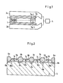
- a solid-state image pick-up device will be generally explained as an example of CCD image pick-up device with reference to Fig. 1.
- a photosensitive section 1 including a plurality of photosensitive elements S 1 , S 2 , S3...S n-2 , S n-1 and S n , a transfer gate electrode 3, two CCD shift registers 2a and 2b and an output circuit 4 are formed on a semiconductor substrate.
- the output circuit 4 may be formed on a different semiconductor substrate, if the CCD shift registers are arranged to externally output an electrical signal.
- Photo carriers are produced and are accumulated in the photosensitive elements S 1 , S 2 , S3...S n-2 , S n-1 and S n , when these elements are exposed to light.
- the transfer gate electrode 3 opens to transfer the carriers accumulated in the respective photosensitive elements to the shift registers 2a and 2b.
- the carriers in the even- numbered photosensitive elements S 2 , S 4 ... are transferred to the shift register 2a, while the carriers in the odd- numbered photosensitive elements S1, S 3 ... are transferred to the shift register 2b.
- the transfer gate electrode 3 closes the gate, and the shift registers 2a and 2b begin to shift the carriers transferred from the respective photosensitive elements to the output circuit 4.
- the carriers shifted along the respective shift registers 2a and 2b are alternately input to the output circuit 4, which converts the amount of carriers into a voltage and outputs successive electrical signals corresponding to -the charges in the respective photosensitive elements in sequence starting from the n-th element.
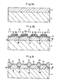
- FIG. 2 is a part-sectional view along the line connecting respective centers of photosensitive elements S 1 , S 2 , S 3 ...S n-2 , S n -1 and S n .
- Each photosensitive element corresponds to one of N-type regions 9a, 9b, 9c and 9d which are disposed on a P-type semiconductor substrate 5.
- the N-type regions 9a, 9b, 9c and 9d are separated from each other by P +- type channel stopper regions 8a, 8b, 8c, 8d and 8e and field insulator layers 6a, 6b, 6c, 6d and 6e having a large thickness.
- P -type channel stopper regions 8a...8e are parts of a continuous region which is formed in a zig-zag or serpentine pattern to allow the charges accumulated in adjacent N-type regions 9a...9d to be taken out in different directions.
- N-type regions 9a, 9b, 9c and 9d are covered by transparent insulator films 7a, 7b, 7c and 7d.
- the field insulator layers 6a, 6c, 6c, 6d and 6e and the insulator films 7a, 7b, 7c and 7d are typically made of silicon oxide.
- the P-type semiconductor substrate 5 and the N-type regions 9a, 9b, 9c and 9d form P-N junctions 10a, lOb, lOc and lOd. Carriers produced by irradiated light are accumulated in depletion layers caused by these P-N junctions 10a, 10b, 10c and 10d.
- the width of the P +- type channel stopper regions 8a ⁇ 8e is usually designed to be slightly above this limit. Therefore, increasing the number of photosensitive elements without increasing the occupation area must be accompanied by decrease in the area of the P-N junctions 10a ⁇ 10d, resulting in the deterioration of sensitivity.
- a ratio of the junction area to cell area (where the cell area is the sum of the areas of the junctions 10a ⁇ 10d and the channel stopper regions 8a ⁇ 8e), which is a so-called quantum efficiency, would be lowered.
- the proportion of photo-carriers which are produced under the channel stopper region becomes high and, since most of these photo-carriers are absorbed through recombination without any contribution to the photoelectric conversion, the photoelectric conversion becomes inefficient.
- some of these photo-carriers are likely to drift to the CCD shift-registers 2a and 2b and the output circuit 4, resulting in a deterioration of the coherence of output with the input light information.
- a semiconductor substrate 5 having an impurity density of about 1 x 1 0 15 cm- 3 is prepared.
- An ion implanation of phosphorous is effected to the substrate 12 -2 with an energy of 100 KeV and a dose of 1 x 10 cm .
- This is followed by an annealing process within a nitrogen atmosphere at 1,100 - 1,200°C to obtain an N-type region 9 having a depth of about 1.5 ⁇ m.
- an oxide layer 11 having a thickness of 500 - 700i is formed on the N-type region 9, and a silicon nitride layer 12 having a thickness of 1,000i is formed on the oxide layer 11 by a CVD (Chemical Vapor Deposition) method.
- a CVD Chemical Vapor Deposition
- photo-resist layers 13a - 13d each having a predetermined shape are formed on the silicon nitride layer 12
- the silicon nitride layer 12 is partly etched away by a plasma etching method using a mask of the photo-resist layers 13a - 13d. This is followed by ion implanation with boron at an energy of 100 KeV and a dose of 1 x 10 13 cm -3 to form P + -type channel stopper regions 8a - 8e.
- field oxide layers 6a ⁇ 6e having a thickness of about 1 ⁇ m are formed in a wet oxygen atmosphere at 1,000°C.
- the remaining silicon nitride layer 12 operates as a mask.for oxidation. This is important in order to retain some thickness of the N-type layer 9 under the P + -type regions. 8a ⁇ 8e whose positions are lowered as a result of the field oxide layer formation.
- new gate oxide layers 7a - 7d of about 1,OOOA are regrown on the surface of the N-type layer 9 between the P + -type channel stopper regions 8a ⁇ 8e to complete the fabrication.
- the regrowth of the new gate oxide layers 7a ⁇ 7d may be omitted while instead leaving the oxide layer 11 between the P + -type channel stopper regions 8a - 8e, since the oxide layer 11 is contaminated during the manufacturing procedure, it is preferable for the electrical characteristics of the photosensitive section to regrow the new gate oxide layers 7a - 7d.
- the N-type layer 9 exists under the P -type regions 8a - 8e so that the P-N junctions between the N-type region 9 and the substrate 5 exists not only under the gate oxide films 7a-7d but also under the channel stopper regions 8a - 8e. Further, since the region 9 is formed under the stopper regions, a P-N junction is also formed between the region 9 and each stopper region 8a-8e.
- each of these additional P-N junctions faces the junction between regions 9 and 5
- the potential profile of the N-type region 9 between these facing P-N junctions has a potential well shallower than that of the N-type region.9 between the channel stopper regions 8a - 8e so that the regions of layer 9 under the stopper regions 8a-8e act as barrier regions to prevent carriers from drifting between adjacent photosensitive regions under the oxide films 7a-7e.
- This shallow potential well not operates as a potential barrier preventing photo-carriers produced in the N-type layer 9 between the channel stopper regions 8a- 8e from drifting to the adjacent regions, but also improves the sensitivity.
- the photo-carriers produced in the N-type layer 9 under the channel stopper regions 8a - 8e drift to the N-type layer 9 between the channel stopper regions 8a- 8e which has a deeper potential well, and these are collected, together with the photo-carriers produced in the N-type layer 9, between the channel stopper regions 8a - 8e.
- the light information irradiated through the channel stopper regions which is ignored in the photosensitive section in the prior art, is effectively used to improve the sensitivity. Due to this fact, the resolution can be improved, without impairing the sensitivity, by increasing the number of photosensitive elements while decreasing the respective areas thereof. Further, since the number of photosensitive elements may be increased without enlarging the overall area of the semiconductor chip, the production yield of the solid-state image pick-up device is not degraded.
- the photo-carriers produced under the channel stoppers 8a - 8e are introduced to the N-type layer 9 between the stopper regions without free diffusion. Therefore, the photo-carriers do not affect the electrical characteristics of the shift registers 2a and 2b and the output circuit 4 (Fig. 1). Thus, an output faithful to the input light information is obtained.
Landscapes
- Solid State Image Pick-Up Elements (AREA)
- Transforming Light Signals Into Electric Signals (AREA)
- Light Receiving Elements (AREA)
Applications Claiming Priority (2)
| Application Number | Priority Date | Filing Date | Title |
|---|---|---|---|
| JP153238/81 | 1981-09-28 | ||
| JP56153238A JPS5854671A (ja) | 1981-09-28 | 1981-09-28 | 固体撮像素子 |
Publications (2)
| Publication Number | Publication Date |
|---|---|
| EP0075924A2 true EP0075924A2 (fr) | 1983-04-06 |
| EP0075924A3 EP0075924A3 (fr) | 1985-04-17 |
Family
ID=15558070
Family Applications (1)
| Application Number | Title | Priority Date | Filing Date |
|---|---|---|---|
| EP82108964A Withdrawn EP0075924A3 (fr) | 1981-09-28 | 1982-09-28 | Dispositif capteur d'image à l'état solide présentant une grande résolution et une grande sensitivité |
Country Status (2)
| Country | Link |
|---|---|
| EP (1) | EP0075924A3 (fr) |
| JP (1) | JPS5854671A (fr) |
Cited By (5)
| Publication number | Priority date | Publication date | Assignee | Title |
|---|---|---|---|---|
| WO1987003140A1 (fr) * | 1985-11-12 | 1987-05-21 | Eastman Kodak Company | Photodiode a grande surface et faible capacitance, et telemetre l'utilisant |
| DE4116694A1 (de) * | 1990-05-31 | 1991-12-05 | Fuji Electric Co Ltd | Mit einer fotodiode versehene halbleitervorrichtung und verfahren zu ihrer herstellung |
| FR2669146A1 (fr) * | 1990-11-09 | 1992-05-15 | Thomson Composants Militaires | Capteur photosensible a photodiodes, notamment a photodiodes de faibles dimensions, et procede de fabrication d'un tel capteur. |
| WO1993000710A1 (fr) * | 1991-06-25 | 1993-01-07 | Dalsa Inc. | Capteur d'images a couplage de charge, de grande vitesse, a large gamme dynamique et hautement photosensible |
| GB2432418A (en) * | 1982-07-02 | 2007-05-23 | Secr Defence | Optical sensing system |
Families Citing this family (2)
| Publication number | Priority date | Publication date | Assignee | Title |
|---|---|---|---|---|
| FR2633101B1 (fr) * | 1988-06-16 | 1992-02-07 | Commissariat Energie Atomique | Photodiode et matrice de photodiodes sur hgcdte et leurs procedes de fabrication |
| US10903258B2 (en) * | 2017-10-11 | 2021-01-26 | Kla Corporation | Image sensors with grounded or otherwise biased channel-stop contacts |
Family Cites Families (2)
| Publication number | Priority date | Publication date | Assignee | Title |
|---|---|---|---|---|
| NL7311600A (nl) * | 1973-08-23 | 1975-02-25 | Philips Nv | Ladingsgekoppelde inrichting. |
| JPS5436126A (en) * | 1977-08-26 | 1979-03-16 | Toshiba Corp | Solidstate pick up device |
-
1981
- 1981-09-28 JP JP56153238A patent/JPS5854671A/ja active Pending
-
1982
- 1982-09-28 EP EP82108964A patent/EP0075924A3/fr not_active Withdrawn
Cited By (8)
| Publication number | Priority date | Publication date | Assignee | Title |
|---|---|---|---|---|
| GB2432418A (en) * | 1982-07-02 | 2007-05-23 | Secr Defence | Optical sensing system |
| GB2432418B (en) * | 1982-07-02 | 2008-01-09 | Secr Defence | Optical sensing systems |
| WO1987003140A1 (fr) * | 1985-11-12 | 1987-05-21 | Eastman Kodak Company | Photodiode a grande surface et faible capacitance, et telemetre l'utilisant |
| DE4116694A1 (de) * | 1990-05-31 | 1991-12-05 | Fuji Electric Co Ltd | Mit einer fotodiode versehene halbleitervorrichtung und verfahren zu ihrer herstellung |
| US5243215A (en) * | 1990-05-31 | 1993-09-07 | Fuji Electric Co., Ltd. | Semiconductor photodiode device with reduced junction area |
| DE4116694C2 (de) * | 1990-05-31 | 2001-10-18 | Fuji Electric Co Ltd | Mit einer Fotodiode versehene Halbleitervorrichtung und Verfahren zu ihrer Herstellung |
| FR2669146A1 (fr) * | 1990-11-09 | 1992-05-15 | Thomson Composants Militaires | Capteur photosensible a photodiodes, notamment a photodiodes de faibles dimensions, et procede de fabrication d'un tel capteur. |
| WO1993000710A1 (fr) * | 1991-06-25 | 1993-01-07 | Dalsa Inc. | Capteur d'images a couplage de charge, de grande vitesse, a large gamme dynamique et hautement photosensible |
Also Published As
| Publication number | Publication date |
|---|---|
| EP0075924A3 (fr) | 1985-04-17 |
| JPS5854671A (ja) | 1983-03-31 |
Similar Documents
| Publication | Publication Date | Title |
|---|---|---|
| US4231149A (en) | Narrow band-gap semiconductor CCD imaging device and method of fabrication | |
| US5191399A (en) | Solid-state imaging device with improved photodetector | |
| EP0247942B1 (fr) | Capteur d'images semi-conducteur et son procédé de fabrication | |
| US5338691A (en) | Method of making a photodiode with reduced junction area | |
| GB2095905A (en) | Infra-red radiation imaging devices and methods for their manufacture | |
| US4742027A (en) | Method of fabricating a charge coupled device | |
| US5238864A (en) | Method of making solid-state imaging device | |
| EP0570090B1 (fr) | Détecteur d'images et son procédé de fabrication | |
| KR950014687B1 (ko) | 고체촬상장치 | |
| US4377904A (en) | Method of fabricating a narrow band-gap semiconductor CCD imaging device | |
| US5210049A (en) | Method of making a solid state image sensor | |
| JPH05226378A (ja) | 電荷転送素子の製法 | |
| JPS6057780A (ja) | 固体撮像装置およびその製造方法 | |
| JPS60263459A (ja) | Ccd画像感知器 | |
| US6338978B1 (en) | Image sensor and method for fabricating the same | |
| US20050145905A1 (en) | Solid-state imaging device and production method of the same | |
| EP0037244A2 (fr) | Procédé de fabrication d'un dispositif de formation d'image semiconducteur utilisant un film photoconducteur | |
| US6333525B1 (en) | Charge transfer apparatus and manufacture method thereof | |
| JPS5854671A (ja) | 固体撮像素子 | |
| JP2842066B2 (ja) | 固体撮像装置及びその製造方法 | |
| JP2000106425A (ja) | 固体撮像素子及びその製造方法 | |
| JPH0465133A (ja) | 電荷結合装置 | |
| JPH03259570A (ja) | 電荷転送素子およびその製造方法 | |
| KR100259064B1 (ko) | Ccd 영상소자 제조방법 | |
| EP0607874A1 (fr) | Détecteur d'image à l'état solide |
Legal Events
| Date | Code | Title | Description |
|---|---|---|---|
| PUAI | Public reference made under article 153(3) epc to a published international application that has entered the european phase |
Free format text: ORIGINAL CODE: 0009012 |
|
| AK | Designated contracting states |
Designated state(s): DE FR GB |
|
| RAP1 | Party data changed (applicant data changed or rights of an application transferred) |
Owner name: NEC CORPORATION |
|
| PUAL | Search report despatched |
Free format text: ORIGINAL CODE: 0009013 |
|
| AK | Designated contracting states |
Designated state(s): DE FR GB |
|
| 17P | Request for examination filed |
Effective date: 19851017 |
|
| 17Q | First examination report despatched |
Effective date: 19861110 |
|
| STAA | Information on the status of an ep patent application or granted ep patent |
Free format text: STATUS: THE APPLICATION HAS BEEN WITHDRAWN |
|
| 18W | Application withdrawn |
Withdrawal date: 19870310 |
|
| RIN1 | Information on inventor provided before grant (corrected) |
Inventor name: ABE, HIROSHIC/O NIPPON ELECTRIC CO., LTD. |