EP0075985B1 - Dispositif de traitement de données pour le traitement de mots de données à symboles multiples, basé sur un code correcteur de symboles et ayant des modes de fonctionnement multiples - Google Patents
Dispositif de traitement de données pour le traitement de mots de données à symboles multiples, basé sur un code correcteur de symboles et ayant des modes de fonctionnement multiples Download PDFInfo
- Publication number
- EP0075985B1 EP0075985B1 EP82201153A EP82201153A EP0075985B1 EP 0075985 B1 EP0075985 B1 EP 0075985B1 EP 82201153 A EP82201153 A EP 82201153A EP 82201153 A EP82201153 A EP 82201153A EP 0075985 B1 EP0075985 B1 EP 0075985B1
- Authority
- EP
- European Patent Office
- Prior art keywords
- code
- symbols
- symbol
- error
- bits
- Prior art date
- Legal status (The legal status is an assumption and is not a legal conclusion. Google has not performed a legal analysis and makes no representation as to the accuracy of the status listed.)
- Expired
Links
Images


Classifications
-
- G—PHYSICS
- G06—COMPUTING OR CALCULATING; COUNTING
- G06F—ELECTRIC DIGITAL DATA PROCESSING
- G06F11/00—Error detection; Error correction; Monitoring
- G06F11/07—Responding to the occurrence of a fault, e.g. fault tolerance
- G06F11/08—Error detection or correction by redundancy in data representation, e.g. by using checking codes
- G06F11/10—Adding special bits or symbols to the coded information, e.g. parity check, casting out 9's or 11's
-
- H—ELECTRICITY
- H03—ELECTRONIC CIRCUITRY
- H03M—CODING; DECODING; CODE CONVERSION IN GENERAL
- H03M13/00—Coding, decoding or code conversion, for error detection or error correction; Coding theory basic assumptions; Coding bounds; Error probability evaluation methods; Channel models; Simulation or testing of codes
- H03M13/03—Error detection or forward error correction by redundancy in data representation, i.e. code words containing more digits than the source words
- H03M13/05—Error detection or forward error correction by redundancy in data representation, i.e. code words containing more digits than the source words using block codes, i.e. a predetermined number of check bits joined to a predetermined number of information bits
- H03M13/13—Linear codes
Definitions
- the invention relates to a data processing device according to the preamble of Claim 1.
- a device of this kind is known from EP-A-0031183 (Application No. 80201185.8) in the name of Applicant.
- the known device specifically concerns a multiprocessor computer system in which the digital data processing is organized according to n parallel processors for each processing the data word and in which the data storage is organized according to n memories which each store one respective code symbol of a resulting code word.
- the known device implements an error-correcting code which can operate in two modes:
- a data-processing device in accordance with the invention is characterized according to the characterizing part of Claim 1.
- the mode register contains n bits, each of which is assigned to a respective code symbol within the code word in order to control the erasure mode for this code symbol. Encoding and decoding of the mode register thus remains simple.
- an error register which comprises at least n bit locations and an eleventh input which is connected in parallel with the third input of the mode register in order to receive, upon detection of a correctable error in a symbol, a symbol indicator which is to be stored in an associated position of the error register, the symbol indicators received being continuously combined with a stored symbol indicator by means of a symbol-wise logic OR-function, the error register having an eleventh output for connection to an updating and control device, and also a reset input for receiving a reset signal from the control device.
- long-term signalling can also be updated. In cases of doubt a more qualified judgement can thus be given concerning the reliability of a symbol having a given sequence number within the code word.
- the mode register has an additional data input and a load control input for receiving a control word from the control device in order to control the data processing device in a gating mode so that a data word is reconstructed by the selective erasure of (n-k) code symbols on the basis of the k code symbols then remaining, without correction of errors.
- the data processing device can thus continue even if (n-k) code symbols or code symbol locations contain more or less permanently unreliable data.
- a detector for detecting a multi-bit one-symbol error in the normal mode and for directly switching over the mode register to the erasure mode in reaction thereto, code symbols having the same symbol number as that in which the multi-bit one-symbol error occurred being subsequently erased. It has been found that such a multi-bit symbol error can be advantageously used to indicate an unreliable code symbol position.
- a multiprocessor system according to the state of the art can be advantageously extended when each sub-system also comprises its own mode register and its own error register for controlling the processing of the code symbols and for temporarily storing a detected error. Comparatively large sections of the system may then exhibit substantial faults for a more or less prolonged period of time, without the operation of the entire system being endangered.
- a symbol consists of a fixed number of, for example, m bits and may then have 2m different values.
- the set of 2m symbols then forms a Galois field GF(2m) for which the algebraic operations are defined; for example, see the article by T. C. Bartee et al, Information and Control, Vol. 61 (1963), pages 79-98.
- Figure 1 shows the sixteen elements of the Galois field GF(2 4 ), that is to say once written as a series of powers and once as respective bit groups.
- the data words in the embodiment described consist of two symbols of four bits; the (redundant) code words consist of four symbols of four bits.
- Figure 2 shows the generator matrix [G] and the parity check matrix [H] whose elements are each four-bit symbols. Multiplication of the parity matrix [H] according to [S] - [H] by a non-singular matrix [S] of 2x2 symbols produces a transformed parity check matrix which imparts the same properties to the code as the original matrix [H].
- W s is the symbol weight of a code word, that is to say the number of symbols of a code word which are not equal to the symbol 0 (0000).
- W b is the bit weight of a symbol, that is to say the number of bits of a symbol which are not equal to 0.
- d s is the symbol weight of the code, that is to say the minimum symbol weight over all code words. In this respect it is assumed that the code words (0000) and the symbol 0 (0000) are permissible. However, the occurrence of the code word (0000) does not influence symbol weight of the code, which is based on the other code words only.
- the code has the following properties:
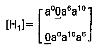
- i may have an arbitrary value (modulo-15), that is to say i e ⁇ 0, 1, 2... 14 ⁇ . It follows directly from the differences between the exponents of a that if one of the exponents has the value 0, 1, 2 or 3, the other two can never have one of these four values.
- modulo-2 sum of a one-symbol error and two one-bit errors could occur only in the following cases:
- Figure 3 shows all possibilities for obtaining, by multiplication of the same matrix, all parity check matrices having the attractive properties described.
- Other (2x2) matrices can also be used for the multiplication, but no systematic codes are then obtained. Even though such codes have exactly the same error-correcting properties, the implementation thereof requires additional components. Further members of the same code family, having, therefore, the same error-correcting properties, can be found by:
- the encoder for such a code implements the multiplication of the data words by the generator matrix (which is derived each time from the parity check matrix in an elementary manner). This multiplication can be performed, for example, by means of a read-only memory (ROM).
- ROM read-only memory
- the decoder is more complex. It has been found that with the systematic codes of Figure 3 the data words can always be reconstructed from an arbitrary set of two (k) undisturbed code symbols. It is advantageous to use this principle for the construction of the decoder.
- Figure 4 first of all shows the formation of the code symbols (c0, c1, c2, c3) from the data symbols (d0, d1) by means of the generator matrix ( Figure 3, second line). Also shown are the formation of feasible sets of two code symbols and, using the inverted generator matrix, the reconstruction of the data symbols from the respective sets of code symbols.
- the set of possibly disturbed code symbols received is multiplied in the decoder by an extended parity check matrix [Q].
- This matrix is shown in Figure 5 and is derived from the original parity check matrix by multiplication by an auxiliary matrix [A].
- the matrix [A] is determined on the basis of the following requirements:
- Combinations which do not satisfy one of the above relations for the syndrome symbols cannot be corrected in the normal mode. Combinations which satisfy one of the above relations for the syndrome symbols, however, may also be due to a non-correctable fault or even by a non-detectable fault.
- the block 102 of Figure 6 thus forms the four syndrome words s0, s1, s2, s3 on its relevant outputs for each code word. These syndrome words are applied to the blocks 104 and 106.
- Block 104 is the data reconstruction device, for which purpose it receives the four syndrome symbols and, moreover the (possibly disturbed) code symbols on input 100.
- the data word Y 32 which has been reconstructed on the basis of only the code symbols c2 and c3 appears on output 108; the same is applicable to the other outputs of the block 104.
- Figure 7a shows the binary representation of the matrix of Figure 7b (a binary representation of such a transformation matrix is customary); each of the "1" bits represents a term which must taken into account for the ultimate result by way of an EXCLUSIVE-OR operation.
- block 106 six signals are derived from the four syndrome symbols received in order to indicate which of the six versions of the data word reconstructed by the block 104 have been derived from non-disturbed code symbols.
- Figure 9 indicates symbolically which logic functions of the syndrome symbols are formed. For example, if the syndrome symbol s1 must form part of the set (a4, a 5 , a°, a'), this symbol is compared bit-wise with each of the four relevant elements of the Galois field GF(2 4 ) of Figure 1. This condition has already been mentioned with respect to the localizing of two one-bit errors. When this condition is satisfied, the corresponding output signal bit in Figure 9 becomes "true".
- the decoder can operate in nine different modes, that is to say:
- Element 110 of Figure 6 is a control and signalling register.
- Figure 10 shows the embodiment comprising a four-bit mode register and the necessary decoding.
- Figure 11 shows the criteria to be satisfied by the signals p and q described and the mode signals to be formed, and also the filling of the error signalling register which also contains four bits.
- the abbreviations used have the following meaning:
- the error is actually not corrected but the appropriate pair of code symbols on the basis of which the data symbols must be recovered is selected by error localization.
- Each correctable error occurs once in the table.
- the case NE (mo errors) occurs twice: the system can thus utilize the first two code symbols (y10) in parallel as well as the last two code symbols (y32) in parallel.
- the AND-gate 116 as well as 118 of the AND-gates 112 to 122 in Figure 6 are conductive (these AND-gates each operate over a width of 8 bits).
- the interface unit 124 comprises, for each bit-line of the 8-bit wide output 126, an OR-gate having six inputs: each of these inputs is fed by a different one of the AND-gates 112 to 122. If there is no error, the two results y32 and y10 are identical. This double definition of the case "NE" saves components as well as time in comparison with other solutions.
- Figure 12 shows the conditions to be satisfied for the respective selections from the data y32, y31, y30, y21, y20, y10; these conditions are first shown as a sum of products which follows directly from the table of Figure 11. Subsequently, they are each shown again as a product of sum terms. This conversion also utilizes the property that the signals RM, EM ; and MOS I , are disjunct: at any instant only one of these eleven signals can be true. These rewritten functions can be realized by means of fewer components and with a small signal delay time.
- the respective circuits for forming the control signals for the gates 112 to 122 in Figure 6 are shown in the Figures 13,14,15, 16, 17, 18. The parts of the functions which depend only on the content of the mode register are shown in Figure 19.
- the error register forming part of the element 110 in Figure 6, contains the following information:
- the mode register serves for the (co) control of the actual operating mode and the selection from the data y32 ... y10.
- both registers comprise as many bit positions as there are code symbols in the code word.
- other choices are also feasible. For example, in a double-length error register of eight bits, one half is used for signalling the one-bit errors and the other half for signalling one-symbol errors. This extended embodiment will not be elaborated upon herein.
- an error-signalling tetrade is supplied to the error register each time in order to be combined bit-wise with the information already stored.
- the word to be supplied to the error register is shown in Figure 11 (extreme right-hand column) which illustrates the relationship between the content of the mode register, the various criteria described and the type of error.
- the selection functions have already been derived from the table of Figure 11. These functions indicate which version (of the six feasible versions) of the data word is to be used.
- the content of the error register is partly.
- Figures 21a ... 21f thus show the functions to be derived from configurations shown in Figures 13, 14, 15, 16, 17, 18, respectively.
- the variable RM, EM and MOS are mutually disjunct: at any given instant, at the most one of these variables can have the value "1".
- Mo... M 3 indicate the values of the relevant mode register bits; a stroke over a variable indicates the inverted value.
- a stroke over a variable indicates the inverted value.
- Figure 23 shows a realization involving twelve AND-gates (&) 2000 ... 222, four OR-gates (OR) 225 ... 230 and a NOR-gate 232 for forming the set conditions.
- the error register comprises four data flipflops 234... 240, whose clock control is not shown. These flipflops also comprise a reset input (not shown).
- the formation of the OR-function between the old content of the data flipflops and a new error-indicating word is realized by means of the OR-gates 242 ... 248. When a detectable, non-correctable error arises, all syndrome symbols SO, S1, S2, S3 are different from zero. On the other hand, no "one" bit is applied to the error register (by way of the preceding OR-functions).
- the error register is periodically read and reset to zero by a supervision device. This does not have a direct effect on the content of the mode register, as will appear hereinafter.
- the supervision device operates, for example, under software control.
- the content of the error register is then used, for example, for long-term updating: the number of error indications occurring over a given period of time is summed for each code symbol.
- the code symbols whose sums are the lowest can then be evaluated as being the most reliable, so that these symbols are used in the gating mode.
- the signalling of an uncorrectable error (gate 232) can be used to generate an interrupt signal or to control a retry. Such retries are customary in data processing devices. The sub-operations required for such a retry depend on the kind of device and the actual data processing; for the sake of brevity, they will not be elaborated upon herein.
- Figure 24 shows a computer system in which the invention is implemented; the interconnection of the sub-systems has already been partly disclosed in said EP-A-0031183 (PHN 9652), be it for use with a less effective error-correcting code.
- the data words consist of 8 bits which are assumed to be two symbols of four bits.
- each data word is processed in each processor and is represented each time by four code bits in the associated memory or on the output of the sub-computer.
- the data words appear on the lines 62, 64, 66, 68. They are processed in the respective processor elements 12, 14, 16, 18.
- the processor elements generate data result words on the lines 90, 92, 94, 96 or address words on the lines 70, 72, 74, 76.
- a known memory management unit may be provided for each of the relevant memories.
- the local memories 28, 30, 32, 34 are addressed via the address decoders 27, 29, 31, 33. From each 8-bit data word received, a 4-bit code symbol is formed in each of the code generators 20, 22, 24, 26, so that the code symbols formed from one data word together form one code word. These code symbols are presented to the memories 28, 30, 32, 34 in order to be stored.
- the code symbols read are regenerated in the read amplifiers 36, 38, 40, 42. The regeneration can alternatively be realized without intermediate storage in the memories.
- the code symbols can all be applied to all registers 46, 48, 50, 52.
- registers are connected to the reconstruction devices or decoders 54, 56, 58, 60 for reconstructing the data words from the code words for presentation to the lines 62, 64, 66, 68.
- the combination of elements 46, 54, 12, 20, 28 and 36 is included in a single separate error isolation zone and correspondingly for further zones. It is assumed that the errors in two different error isolation zones are independent; in many cases this requirement is satisfied for many categories of errors if each error-isolation zone covers, for example, a separate printed circuit board plus components, or alternatively a separate integrated circuit.
- the circuit shown in the Figure thus forms four respective error isolation zones. The synchronization of the operations in the four error isolation zones has been omitted for the sake of clarity.
- the processors operate in accordance with relevant programs.
- the data reconstruction device may be constructed in accordance with the principle described with reference to Figure 6.
- FAA selectable error isolation zone
- the normal mode which is capable of correcting two arbitrarily situated bit errors or a one-symbol error is very well suited for the correction of errors occurring in the memory. These latter errors usually are mutually independent and, moreover, are often so-called "soft errors”.
- Symbol errors which render an entire symbol unreliable are usually caused by a faulty processor. It has been found that such symbol errors are usually of a permanent nature. However, they need not be repaired at short notice in this computer system, because the decoders can switch over to the erasure mode.
- each error-isolation zone in Figure 24 comprises a separate error register (148, 150, 152, 154) which is controlled by output signals from the relevant decoder (54, 56, 58, 60) and whose output signals are applied to the central control device 44. Finally there are shown the relevant reset lines for the error registers from the central control unit 44. The multiplicity of these control lines is not shown.
- each error-isolation zone in Figure 24 comprises a respective 4-bit mode register 140, 142, 144, 146.
- the mode registers are controlled by output signals from the associated decoders (54, 56, 58, 60).
- the content of each mode register controls the operating mode of the associated decoder.
- the setting of the error register is co-controlled by the content of the associated mode register. This relation is indicated each time by an additional arrow (parts of the circuit of Figure 23 would thus be situated in the error register in Figure 24).
- each mode register receives control signals from the central control device 44. The composition of these control lines will be described hereinafter. In the error-free condition, the same program is executed in all isolation zones. This is also applicable in the normal mode.
- Figure 25 shows the four-bit mode register and the associated control circuit.
- the condition signals are formed for the relevant mode bits by means of the four AND-gates 250 ... 256. These condition signals are applied, via the OR-gates 258... 264, to the register proper which is formed by four data flip-flops 266 ... 272. The clock control of these data flipflops is not shown separately.
- the output data are combined in NOR-gate 274: the output signal thereof (RM) indicates the normal mode.
- the circuit furthermore comprises an additional control input 276 and a four-bit data input 278.
- four AND-gates 280-286 random external information can be input, for example, under the control of the residential software of the control device 44 of Figure 24. For example, the gating mode can be initiated under the influence of the long-term updating of the detected errors.
- a "1" signal on the control input 288 then acts as an enable signal. This signal may be formed only in given data processing phases, for example when all detection signals (p,, SEL jj ) have come to a rest.
- Figure 26 shows a first alternative for the decoder, which alternative utilizes a preprogrammed read-only memory (ROM).
- ROM read-only memory
- an 8-bit syndrome is formed from the 16-bit code word by means of an exclusive OR-matrix (300). This syndrome contains the complete information concerning the error. Therefore, an 8-bit correction word can be formed by means of a read-only memory 302. This correction word can be added bit-wise modulo-2 to the two data symbols (304) in order to reconstruct the non-disturbed data word.
- the four signal bits to be applied to the error register 306 are to be formed at the same time. Since the system can operate in different modes, the read-only memory must also receive the four bits from the mode register 308, because the interpretation of the syndrome is co-determined by the mode.
- Figure 25 also shows the binary version of the parity check matrix. This can be implemented by means of 38 two-input EXCLUSIVE OR gates. When these gates are arranged in a tree-like configuration, the implementation of this matrix introduces a delay of only three gate delay times. The interaction between mode register and error register takes place in the manner of Figure 23 and is not shown separately; the further control of the mode register 308 is not shown separately either. It is alternatively possible to implement the parity check matrix with a further read-only memory.
Landscapes
- Engineering & Computer Science (AREA)
- Theoretical Computer Science (AREA)
- Physics & Mathematics (AREA)
- Quality & Reliability (AREA)
- General Engineering & Computer Science (AREA)
- General Physics & Mathematics (AREA)
- Probability & Statistics with Applications (AREA)
- Error Detection And Correction (AREA)
- Detection And Correction Of Errors (AREA)
- Detection And Prevention Of Errors In Transmission (AREA)
- Hardware Redundancy (AREA)
- Multi Processors (AREA)
Claims (8)



Priority Applications (1)
| Application Number | Priority Date | Filing Date | Title |
|---|---|---|---|
| AT82201153T ATE14947T1 (de) | 1981-09-21 | 1982-09-17 | Datenverarbeitungsvorrichtung zur verarbeitung von datenwoertern mit mehreren symbolen, auf einem symbolkorrigierenden kode basiert und mit mehreren betriebsweisen. |
Applications Claiming Priority (2)
| Application Number | Priority Date | Filing Date | Title |
|---|---|---|---|
| NL8104342A NL8104342A (nl) | 1981-09-21 | 1981-09-21 | Rekenmachinesysteem, gebaseerd op een symboolkorrigerende kode met twee werkmodes. |
| NL8104342 | 1981-09-21 |
Publications (2)
| Publication Number | Publication Date |
|---|---|
| EP0075985A1 EP0075985A1 (fr) | 1983-04-06 |
| EP0075985B1 true EP0075985B1 (fr) | 1985-08-14 |
Family
ID=19838096
Family Applications (1)
| Application Number | Title | Priority Date | Filing Date |
|---|---|---|---|
| EP82201153A Expired EP0075985B1 (fr) | 1981-09-21 | 1982-09-17 | Dispositif de traitement de données pour le traitement de mots de données à symboles multiples, basé sur un code correcteur de symboles et ayant des modes de fonctionnement multiples |
Country Status (8)
| Country | Link |
|---|---|
| US (1) | US4512020A (fr) |
| EP (1) | EP0075985B1 (fr) |
| JP (1) | JPS58127252A (fr) |
| AT (1) | ATE14947T1 (fr) |
| AU (1) | AU552984B2 (fr) |
| CA (1) | CA1190655A (fr) |
| DE (1) | DE3265431D1 (fr) |
| NL (1) | NL8104342A (fr) |
Families Citing this family (31)
| Publication number | Priority date | Publication date | Assignee | Title |
|---|---|---|---|---|
| NL8204038A (nl) * | 1982-10-20 | 1984-05-16 | Philips Nv | Multiprocessorrekenmachinesysteem, bevattende n parallel werkende rekenmachinemodules, en rekenmachinemodule te gebruiken in zo een multiprocessorrekenmachinesysteem. |
| NL8400630A (nl) * | 1984-02-29 | 1985-09-16 | Philips Nv | Decodeerinrichting voor een stroom van codesymbolen die woordsgewijze beschermd zijn door een dubbele reed-solomon-code met een minimum hamming-afstand van 5 over de codesymbolen en een verbladeringsmechanisme tussen de beide codes, alsmede speler voorzien van zo een decodeerinrichting. |
| NL8403147A (nl) * | 1984-10-16 | 1986-05-16 | Philips Nv | Dataverwerkingssysteem dat is opgebouwd uit drie dataverwerkingsmodules. |
| US4835713A (en) * | 1985-08-06 | 1989-05-30 | Pitney Bowes Inc. | Postage meter with coded graphic information in the indicia |
| GB2189970B (en) * | 1986-05-01 | 1990-03-28 | British Broadcasting Corp | Data conversion |
| GB2194850B (en) * | 1986-09-05 | 1990-10-31 | Philips Nv | Data processing device |
| DE3752367T2 (de) * | 1986-09-30 | 2004-02-19 | Canon K.K. | Fehlerkorrekturgerät |
| US4775978A (en) * | 1987-01-12 | 1988-10-04 | Magnetic Peripherals Inc. | Data error correction system |
| JPS649539A (en) * | 1987-07-02 | 1989-01-12 | Hitachi Denshi Service Kk | Protecting method for storing data |
| JP2881773B2 (ja) * | 1988-07-30 | 1999-04-12 | ソニー株式会社 | 誤り訂正装置 |
| EP0386506A3 (fr) * | 1989-03-06 | 1991-09-25 | International Business Machines Corporation | Codage et décodage de symboles à correction d'erreurs à peu de frais |
| EP0481128B1 (fr) * | 1990-10-16 | 1998-01-14 | Koninklijke Philips Electronics N.V. | Système de traitement de données basé sur un code de symbole (N,K) avec possibilités de correction d'erreurs des symboles et de réparation d'erreurs multiples |
| EP0597511B1 (fr) * | 1992-10-09 | 1999-04-07 | Koninklijke Philips Electronics N.V. | Méthode de correction d'erreurs et d'éffacements d'information digitals, et dispositif approprié à la mise en oeuvre du procédé |
| US6118873A (en) * | 1998-04-24 | 2000-09-12 | International Business Machines Corporation | System for encrypting broadcast programs in the presence of compromised receiver devices |
| FR2814612B1 (fr) * | 2000-09-26 | 2003-02-07 | St Microelectronics Sa | Code de detection et/ou de correction d'erreurs a haute efficacite |
| US9520993B2 (en) | 2001-01-26 | 2016-12-13 | International Business Machines Corporation | Renewable traitor tracing |
| US8108429B2 (en) * | 2004-05-07 | 2012-01-31 | Quest Software, Inc. | System for moving real-time data events across a plurality of devices in a network for simultaneous data protection, replication, and access services |
| US7565661B2 (en) | 2004-05-10 | 2009-07-21 | Siew Yong Sim-Tang | Method and system for real-time event journaling to provide enterprise data services |
| US7680834B1 (en) | 2004-06-08 | 2010-03-16 | Bakbone Software, Inc. | Method and system for no downtime resychronization for real-time, continuous data protection |
| US7681104B1 (en) | 2004-08-09 | 2010-03-16 | Bakbone Software, Inc. | Method for erasure coding data across a plurality of data stores in a network |
| US7681105B1 (en) * | 2004-08-09 | 2010-03-16 | Bakbone Software, Inc. | Method for lock-free clustered erasure coding and recovery of data across a plurality of data stores in a network |
| US8046661B2 (en) * | 2004-09-08 | 2011-10-25 | Temarylogic Llc | Symbol error correction by error detection and logic based symbol reconstruction |
| US7979404B2 (en) | 2004-09-17 | 2011-07-12 | Quest Software, Inc. | Extracting data changes and storing data history to allow for instantaneous access to and reconstruction of any point-in-time data |
| US7904913B2 (en) | 2004-11-02 | 2011-03-08 | Bakbone Software, Inc. | Management interface for a system that provides automated, real-time, continuous data protection |
| US7788521B1 (en) | 2005-07-20 | 2010-08-31 | Bakbone Software, Inc. | Method and system for virtual on-demand recovery for real-time, continuous data protection |
| US7689602B1 (en) * | 2005-07-20 | 2010-03-30 | Bakbone Software, Inc. | Method of creating hierarchical indices for a distributed object system |
| WO2008076214A2 (fr) * | 2006-12-14 | 2008-06-26 | Regents Of The University Of Minnesota | Détection d'erreur et correction faisant appel à des codes de correction de configuration d'erreurs |
| US8131723B2 (en) | 2007-03-30 | 2012-03-06 | Quest Software, Inc. | Recovering a file system to any point-in-time in the past with guaranteed structure, content consistency and integrity |
| US8364648B1 (en) | 2007-04-09 | 2013-01-29 | Quest Software, Inc. | Recovering a database to any point-in-time in the past with guaranteed data consistency |
| JP5665725B2 (ja) * | 2011-12-13 | 2015-02-04 | 株式会社東芝 | 符号化装置及びこれを用いた半導体メモリシステム |
| JP2023045450A (ja) * | 2021-09-22 | 2023-04-03 | キオクシア株式会社 | シンドローム計算回路、誤り訂正回路およびメモリシステム |
Family Cites Families (8)
| Publication number | Priority date | Publication date | Assignee | Title |
|---|---|---|---|---|
| US4077028A (en) * | 1976-06-14 | 1978-02-28 | Ncr Corporation | Error checking and correcting device |
| GB1597218A (en) * | 1976-12-11 | 1981-09-03 | Nat Res Dev | Apparatus for electronic encypherment of digital data |
| US4117458A (en) * | 1977-03-04 | 1978-09-26 | Grumman Aerospace Corporation | High speed double error correction plus triple error detection system |
| NL7909178A (nl) * | 1979-12-20 | 1981-07-16 | Philips Nv | Rekenmachine met verspreide redundantie welke is verdeeld over verschillende isolatiegebieden voor fouten. |
| US4355391A (en) * | 1980-03-31 | 1982-10-19 | Texas Instruments Incorporated | Apparatus and method of error detection and/or correction in a data set |
| CA1170776A (fr) * | 1980-07-18 | 1984-07-10 | Yoichiro Sako | Methode de correction d'erreurs dans des blocs de donnees |
| US4382300A (en) * | 1981-03-18 | 1983-05-03 | Bell Telephone Laboratories Incorporated | Method and apparatus for decoding cyclic codes via syndrome chains |
| US4414667A (en) * | 1981-11-27 | 1983-11-08 | Gte Products Corporation | Forward error correcting apparatus |
-
1981
- 1981-09-21 NL NL8104342A patent/NL8104342A/nl not_active Application Discontinuation
-
1982
- 1982-09-13 US US06/416,992 patent/US4512020A/en not_active Expired - Lifetime
- 1982-09-17 DE DE8282201153T patent/DE3265431D1/de not_active Expired
- 1982-09-17 AT AT82201153T patent/ATE14947T1/de not_active IP Right Cessation
- 1982-09-17 EP EP82201153A patent/EP0075985B1/fr not_active Expired
- 1982-09-17 CA CA000411702A patent/CA1190655A/fr not_active Expired
- 1982-09-21 JP JP57164813A patent/JPS58127252A/ja active Granted
- 1982-09-21 AU AU88592/82A patent/AU552984B2/en not_active Ceased
Also Published As
| Publication number | Publication date |
|---|---|
| ATE14947T1 (de) | 1985-08-15 |
| CA1190655A (fr) | 1985-07-16 |
| EP0075985A1 (fr) | 1983-04-06 |
| AU552984B2 (en) | 1986-06-26 |
| DE3265431D1 (en) | 1985-09-19 |
| JPH045214B2 (fr) | 1992-01-30 |
| JPS58127252A (ja) | 1983-07-29 |
| AU8859282A (en) | 1983-03-31 |
| US4512020A (en) | 1985-04-16 |
| NL8104342A (nl) | 1983-04-18 |
Similar Documents
| Publication | Publication Date | Title |
|---|---|---|
| US4512020A (en) | Data processing device for processing multiple-symbol data-words based on a symbol-correcting code and having multiple operating modes | |
| US4402045A (en) | Multi-processor computer system | |
| US5754563A (en) | Byte-parallel system for implementing reed-solomon error-correcting codes | |
| US4486882A (en) | System for transmitting binary data via a plurality of channels by means of a convolutional code | |
| EP0026516B1 (fr) | Appareil pour le traitement d'un flot d'information à l'aide d'un code correcteur d'erreur convolutionnel et pour la détection d'une erreur irrémédiable dans ce traitement | |
| US4928280A (en) | Fast processor for multi-bit error correction codes | |
| US5856987A (en) | Encoder and decoder for an SEC-DED-S4ED rotational code | |
| US4504948A (en) | Syndrome processing unit for multibyte error correcting systems | |
| US6219817B1 (en) | Error correction and detection for faults on time multiplexed data lines | |
| JP2612000B2 (ja) | データ処理装置 | |
| US6519736B1 (en) | Generating special uncorrectable error codes for failure isolation | |
| US4633472A (en) | Multiprocessor computer system comprising n parallel operating computer modules, and computer module for use in such a multiprocessor computer system | |
| US6539513B1 (en) | Dual functioning symbol error correction code | |
| US5745507A (en) | Systematic symbol level ECC for use in digital memory systems | |
| US7093183B2 (en) | Symbol level error correction codes which protect against memory chip and bus line failures | |
| Gils | A triple modular redundancy technique providing multiple-bit error protection without using extra redundancy | |
| US5956351A (en) | Dual error correction code | |
| Bruck et al. | New techniques for constructing EC/AUED codes | |
| US5754562A (en) | Method and apparatus for encoding certain double-error correcting and triple-error detecting codes | |
| US9191029B2 (en) | Additional error correction apparatus and method | |
| US6405339B1 (en) | Parallelized programmable encoder/syndrome generator | |
| EP0481128B1 (fr) | Système de traitement de données basé sur un code de symbole (N,K) avec possibilités de correction d'erreurs des symboles et de réparation d'erreurs multiples | |
| EP0341851A2 (fr) | Méthode et appareil de codage entrelacé | |
| EP0178726B1 (fr) | Système de traitement de données composé de trois modules de traitement de données | |
| Stiffler | Coding for random-access memories |
Legal Events
| Date | Code | Title | Description |
|---|---|---|---|
| PUAI | Public reference made under article 153(3) epc to a published international application that has entered the european phase |
Free format text: ORIGINAL CODE: 0009012 |
|
| 17P | Request for examination filed |
Effective date: 19830121 |
|
| AK | Designated contracting states |
Designated state(s): AT BE DE FR GB IT NL SE |
|
| ITF | It: translation for a ep patent filed | ||
| GRAA | (expected) grant |
Free format text: ORIGINAL CODE: 0009210 |
|
| AK | Designated contracting states |
Designated state(s): AT BE DE FR GB IT NL SE |
|
| REF | Corresponds to: |
Ref document number: 14947 Country of ref document: AT Date of ref document: 19850815 Kind code of ref document: T |
|
| REF | Corresponds to: |
Ref document number: 3265431 Country of ref document: DE Date of ref document: 19850919 |
|
| ET | Fr: translation filed | ||
| PLBE | No opposition filed within time limit |
Free format text: ORIGINAL CODE: 0009261 |
|
| STAA | Information on the status of an ep patent application or granted ep patent |
Free format text: STATUS: NO OPPOSITION FILED WITHIN TIME LIMIT |
|
| 26N | No opposition filed | ||
| PGFP | Annual fee paid to national office [announced via postgrant information from national office to epo] |
Ref country code: BE Payment date: 19890912 Year of fee payment: 8 |
|
| PGFP | Annual fee paid to national office [announced via postgrant information from national office to epo] |
Ref country code: AT Payment date: 19890920 Year of fee payment: 8 |
|
| PGFP | Annual fee paid to national office [announced via postgrant information from national office to epo] |
Ref country code: NL Payment date: 19890930 Year of fee payment: 8 |
|
| PG25 | Lapsed in a contracting state [announced via postgrant information from national office to epo] |
Ref country code: AT Effective date: 19900917 |
|
| PG25 | Lapsed in a contracting state [announced via postgrant information from national office to epo] |
Ref country code: BE Effective date: 19900930 |
|
| BERE | Be: lapsed |
Owner name: N.V. PHILIPS' GLOEILAMPENFABRIEKEN Effective date: 19900930 |
|
| PG25 | Lapsed in a contracting state [announced via postgrant information from national office to epo] |
Ref country code: NL Effective date: 19910401 |
|
| NLV4 | Nl: lapsed or anulled due to non-payment of the annual fee | ||
| ITTA | It: last paid annual fee | ||
| EAL | Se: european patent in force in sweden |
Ref document number: 82201153.2 |
|
| ITPR | It: changes in ownership of a european patent |
Owner name: CAMBIO RAGIONE SOCIALE;PHILIPS ELECTRONICS N.V. |
|
| REG | Reference to a national code |
Ref country code: FR Ref legal event code: CD |
|
| REG | Reference to a national code |
Ref country code: FR Ref legal event code: CD |
|
| PGFP | Annual fee paid to national office [announced via postgrant information from national office to epo] |
Ref country code: FR Payment date: 20000925 Year of fee payment: 19 |
|
| PGFP | Annual fee paid to national office [announced via postgrant information from national office to epo] |
Ref country code: SE Payment date: 20000926 Year of fee payment: 19 |
|
| PGFP | Annual fee paid to national office [announced via postgrant information from national office to epo] |
Ref country code: GB Payment date: 20000929 Year of fee payment: 19 |
|
| PGFP | Annual fee paid to national office [announced via postgrant information from national office to epo] |
Ref country code: DE Payment date: 20001122 Year of fee payment: 19 |
|
| PG25 | Lapsed in a contracting state [announced via postgrant information from national office to epo] |
Ref country code: GB Free format text: LAPSE BECAUSE OF NON-PAYMENT OF DUE FEES Effective date: 20010917 |
|
| PG25 | Lapsed in a contracting state [announced via postgrant information from national office to epo] |
Ref country code: SE Free format text: LAPSE BECAUSE OF NON-PAYMENT OF DUE FEES Effective date: 20010918 |
|
| REG | Reference to a national code |
Ref country code: GB Ref legal event code: IF02 |
|
| PG25 | Lapsed in a contracting state [announced via postgrant information from national office to epo] |
Ref country code: DE Free format text: LAPSE BECAUSE OF NON-PAYMENT OF DUE FEES Effective date: 20020501 |
|
| EUG | Se: european patent has lapsed |
Ref document number: 82201153.2 |
|
| GBPC | Gb: european patent ceased through non-payment of renewal fee |
Effective date: 20010917 |
|
| PG25 | Lapsed in a contracting state [announced via postgrant information from national office to epo] |
Ref country code: FR Free format text: LAPSE BECAUSE OF NON-PAYMENT OF DUE FEES Effective date: 20020531 |
|
| REG | Reference to a national code |
Ref country code: FR Ref legal event code: ST |