EP0076099A2 - Circuit TTL - Google Patents
Circuit TTL Download PDFInfo
- Publication number
- EP0076099A2 EP0076099A2 EP82305013A EP82305013A EP0076099A2 EP 0076099 A2 EP0076099 A2 EP 0076099A2 EP 82305013 A EP82305013 A EP 82305013A EP 82305013 A EP82305013 A EP 82305013A EP 0076099 A2 EP0076099 A2 EP 0076099A2
- Authority
- EP
- European Patent Office
- Prior art keywords
- transistor
- circuit
- electrode
- ttl
- buffer
- Prior art date
- Legal status (The legal status is an assumption and is not a legal conclusion. Google has not performed a legal analysis and makes no representation as to the accuracy of the status listed.)
- Granted
Links
Images

Classifications
-
- H—ELECTRICITY
- H03—ELECTRONIC CIRCUITRY
- H03K—PULSE TECHNIQUE
- H03K19/00—Logic circuits, i.e. having at least two inputs acting on one output; Inverting circuits
- H03K19/0008—Arrangements for reducing power consumption
- H03K19/001—Arrangements for reducing power consumption in bipolar transistor circuits
-
- H—ELECTRICITY
- H03—ELECTRONIC CIRCUITRY
- H03K—PULSE TECHNIQUE
- H03K19/00—Logic circuits, i.e. having at least two inputs acting on one output; Inverting circuits
- H03K19/02—Logic circuits, i.e. having at least two inputs acting on one output; Inverting circuits using specified components
- H03K19/08—Logic circuits, i.e. having at least two inputs acting on one output; Inverting circuits using specified components using semiconductor devices
- H03K19/082—Logic circuits, i.e. having at least two inputs acting on one output; Inverting circuits using specified components using semiconductor devices using bipolar transistors
- H03K19/088—Transistor-transistor logic
Definitions
- the present invention relates to a transistor--transistor logic 1TTL) circuit. More particularly, it relates to a TTL inverter having a transient state of a high impedance output for reducing the transient current.
- Transistor-transistor logic inverters are generally used as basic elements in semiconductor integrated circuits. Inverters constructed by PNP transistors or NPN transistors are known. In the following description, TTL inverters constructed with NPN transistors are explained. However, the present invention is also applicable to TTL inverters constructed with PNP transistors.
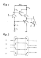
- a conventional TTL inverter comprises a single phase--splitter transistor for splitting the phase of an input signal, which is applied to the base of the phase splitter transistor, into a noninverted phase given at its emitter and an inverted phase given at its ccllector; an inverted signal output transistor for inverting the signal of the noninverted phase; and an off buffer circuit connected in series with the inverting transistor and for receiving the inverted phase signal from the collector of the phase splitter transistor, whereby input signal applied to the input end is inverted and output at the output end.
- the off buffer circuit and the inverted signal output transistor are alternatively turned on and off in response to the outputs of the phase splitter transistor.
- a conventional TTL inverter requires a non-inventing gate connected between the collector of the phase splitter transistor and the off buffer circuit.
- the non-inverting gate comprises .a number of elements. Because of the number of elements, the conventional TTL inverter of this type has a low integration degree and a low operating speed.
- a TTL circuit comprising an input end for receiving an input signal, an output end for providing a logic output in response to the input signal, an inverted signal output circuit including a first transistor having a first control electrode connected to the input end and a second transistor connected between the first transistor and the output end, the inverted signal output circuit having a first threshold voltage and being turned on when the input signal is at a high logic level to make the output end a low logic level, an off-buffer circuit connected to the output end, the off-buffer circuit being turned on to make the output end a high logic level when the input signals are at a low logic level, and an off-buffer driving circuit comprising a third transistor connected between the input end and the off-buffer circuit and having a second control electrode connected to the input end, the off-buffer driving circuit having a second threshold voltage lower than the first threshold voltage of the inverted signal output circuit, whereby the off-buffer circuit is turned off before the turning on of theinverted signal output circuit and is turned on after the inverted signal
- An embodiment of the present invention can provide a TTL circuit which prevents the flow of transient current therethrough.
- An embodiment of the present invention can provide a TTL circuit such that error operations in various circuits having a common power supply line with the TTL circuit (the error operations being caused by the fluctuation of the power supply voltage due to the transient current flowing through the TTL circuit) are prevented.
- An embodiment of the present invention can provide a TTL circuit with reduced power consumption.
- An embodiment of the present invention can provide for an increase in the integration degree in a TTL circuit.
- An embodiment of the present invention can provide for an increase in the operating speed of the TTL circuit.
- Tr is a phase splitter transistor, the base of which operatively receives an input signal applied to an input end A connected to its base, the collector C of which provides an output having a phase inverted from that of the input signal, and the emitter of which provides another output having the same phase as the input signal.
- Transistors-Tr 2 and Tr 3 in a Darlington connection constitute an off buffer circuit. "Off buffer" circuit will be described later.
- a transistor Tr 4 connected in series with the transistor Tr 3 is an inverted signal output transistor, the base B of which is connected to the emitter of the phase splitter transistor Tr l .
- a diode D 1 and a resistor R 1 are connected in series.
- the diode D 1 and the resistor R 1 function to increase the switching speed of the inverted signal output transistor Tr 4 when it turns off, by drawing charges on its base to ground.
- An output end D is connected to a node commonly connected to the emitter of the transistor Tr 3 and the collector of the transistor Tr 4 .
- a capacitor Cc connected to the output end D is a load capacitor of the output line.
- a load resistor L is connected to the output end D.
- Vcc is power supply potential
- R 2 and R 3 are resistors.
- phase splitter transistor Tr 1 When the input signal applied to the input end A is at the "H”level, the phase splitter transistor Tr 1 is in the on state so that its collector C is at the “L” level and its emitter connected to the base B of the inverted signal output transistor Tr 4 is at the “H” level. Accordingly, the output end D is at the "L" level.
- V BE (about 0.8 V) is the base-emitter voltage when the transistor Tr 1 , Tr 2 , Tr 3 , or Tr 4 is conductive
- V CE is the collector-emitter voltage of the transistor when it is saturated
- V f (about 0.5 V), which is lower than V BE , is the anode--cathode voltage of the diode D 1 when it is conductive.
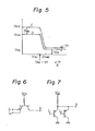
- the transistors Tr 2 and Tr 3 are conductive, and the transistor Tr 4 is not conductive, with the result that the output potential at the output end D is at a high logic level VOH , which is nearly equal to V CC - 2V BE , i.e., the base potential of the transistor Tr 2 minus the base-emitter voltage of the two stages of the transistors Tr 2 and Tr 3 .
- the transistor Tr l begins to be turned on so that the potential at its collector C begins to be lowered, and, accordingly, the transistors Tr 2 and Tr 3 become unsaturated, with the result that the potential at the output end D is gradually lowered.
- the transistors; Tr 1 and Tr 4 are saturated so that they are completely turned on, with the result that the potential at the collector C is lowered to the sum of the collector-emitter voltage V CE of the transistor Tr 1 and the base-emitter voltage of the transistor Tr 4 and the potential at the output end D is lowered to the collector-emitter voltage V CE of the transistor Tr 4 .
- FIG. 3 illustrates input voltage at the input end A going higher than 2V BE , it cannot be increased to higher than 2 VBE because it is clamped to 2V BE by the on--state transistors Tr 1 and Tr 4 .
- the primary object of the present invention is to prevent the above-mentioned instantaneous current from flowing through the transistors Tr 3 and Tr 4 during a transient period.
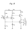
- Fig. 4 the main difference between the conventional circuit of Fig. 1 and the circuit of Fig. 4 is that, in Fig. 4, instead of the single-phase splitter transistor Tr l in Fig. 1, two transistors Tr 5 and Tr 6 are employed.
- the transistor Tr 5 is used for driving only the inverted signal output transistor Tr 4 .
- the transistor Tr 6 is used for driving only the off buffer circuit, including the transistors Tr 2 and Tr 3 .
- the base of the transistor Tr 5 is connected to the input end A, its collector is connected through a resistor R 4 to the power supply line V CC , and its emitter is connected to the base of the inverted signal output transistor Tr 4 and, through a diode D 2 and a resistor R 6 connected in series for drawing the charges on the base of the transistor Tr 4 when it turns on, to the ground.
- a single resistor may alternatively be used.
- the base of the transistor T r6 is connected through a resistor R s to the input end A, its collector is connected to the base of the transistor Tr 2 in the.off buffer circuit and, through a load resistor R 2 , to the power supply line V CC , and its emitter is connected through a diode D 3 to the ground.
- the resistor R 5 is provided for preventing the base potential of the transistor Tr 6 from being clamped to V BE + V f . That is, by providing the resistor R 5 , the potential at the input end A can be increased to 2V BE .
- the transistors Tr 2 and Tr 3 constituting the off buffer circuit, the inverted signal output transistor Tr 4 , the load capaci- tanceCc, and the load resistance L are the same as those in the circuit of Fig. 1.
- the transistors Tr 2 and Tr 3 are in the on state as long as the transistor Tr 6 is not saturated. Therefore, the potential at the emitter of the transistor Tr 3 connected to the output end D is lowered, as is the potential at the base of the transistor Tr 2 connected to the collector C of the transistor Tr 6 .
- the transistor Tr 2 is not supplied with the base current so that the transistor Tr 2 and then the transistor Tr 3 are turned off.
- the transistor Tr 4 is turned on so that the output potential at the output end D is clamped to the low logic level V OL equal to V CE of the transistor Tr 4 . Since the transistor Tr 3 is in the off state after the transistor Tr 6 is saturated, no transient current flows through the transistors Tr 3 and Tr 4 .
- the transistor Tr 4 is first turned off and then the transistor Tr6 is turned off. Accordingly, the transistor Tr 3 is turned on only after the transistor Tr 4 is turned off. Thus, in this case also, no transient current flows through the transistors Tr 3 and Tr 4 .
- a multiemitter transistor as illustrated in Fig. 6, or an AND circuit comprising the PNP transistors, as illustrated in Fig. 7, may be connected.
- I 1 and I 2 are input terminals.
- Schottky barrier transistors are employed as the transistors Tr 2 , Tr 4 , Tr 5 , and Tr 6 .
- the scope of the present invention also covers the case when these transistors are not Schottky barrier transistors.
- the transistors Tr 2 through Tr 6 may alternatively be PNP transistors.
- barrier diode D 3 a conventional transistor having a base--emitter voltage lower than V BE may be used by connecting its collector to its base.
- Figure 8 shows another embodiment of the present invention.
- the single transistor Tr 3 instead of the two transistors Tr 2 and Tr 3 of the off buffer circuit in Fig. 4, constitutes an off buffer circuit.
- the high logic level at the output end D of Fig. 8 is nearly equal to V CC - V DE , which is higher by V BE than the high logic level V CC - 2V BE at the output end D of Fig. 4.
- a TTL inverter having such a high "H" level output cannot be formed as simply as the circuit of Fig. 8. That is, in Fig.
- the circuit 90 acts as a noninverting gate.
- the noninverting gate 90 comprises a number of elements such as transistors Tr 91 , Tr 92 , and Tr 93 , resistors R 91 , R 92 , and R 93 , and a diode D 91 .
- transistors Tr 91 , Tr 92 , and Tr 93 resistors R 91 , R 92 , and R 93
- a diode D 91 As mentioned before, such a number of elements as the above-mentioned ones not only deteriorate the in-, tegration degree but also lower the operating speed.
- a TTL inverter by separately providing two transistors for driving an off buffer circuit and for driving an inverted signal output transistor, respectively, and by making the input threshold voltage for turning on or off the one transistor different from that of another transistor, no transient current flows through the TTL inverter so that fluctuation of the power supply voltage due to the transient current can be prevented. Consequently, error operations of various circuits having a common power supply line with the TTL inverter can be prevented.
- a TTL inverter having a relatively high "H" level output can easily be formed without decreasing the integration degree and the operating speed.
Landscapes
- Engineering & Computer Science (AREA)
- Physics & Mathematics (AREA)
- Computer Hardware Design (AREA)
- Computing Systems (AREA)
- General Engineering & Computer Science (AREA)
- Mathematical Physics (AREA)
- Power Engineering (AREA)
- Logic Circuits (AREA)
Applications Claiming Priority (4)
| Application Number | Priority Date | Filing Date | Title |
|---|---|---|---|
| JP152674/81 | 1981-09-26 | ||
| JP15267481A JPS5853227A (ja) | 1981-09-26 | 1981-09-26 | 論理回路 |
| JP151999/81 | 1981-09-28 | ||
| JP15199981A JPS5854732A (ja) | 1981-09-28 | 1981-09-28 | Ttl論理回路 |
Publications (3)
| Publication Number | Publication Date |
|---|---|
| EP0076099A2 true EP0076099A2 (fr) | 1983-04-06 |
| EP0076099A3 EP0076099A3 (en) | 1984-05-16 |
| EP0076099B1 EP0076099B1 (fr) | 1987-03-25 |
Family
ID=26481052
Family Applications (1)
| Application Number | Title | Priority Date | Filing Date |
|---|---|---|---|
| EP82305013A Expired EP0076099B1 (fr) | 1981-09-26 | 1982-09-23 | Circuit TTL |
Country Status (3)
| Country | Link |
|---|---|
| US (1) | US4562364A (fr) |
| EP (1) | EP0076099B1 (fr) |
| DE (1) | DE3275895D1 (fr) |
Cited By (2)
| Publication number | Priority date | Publication date | Assignee | Title |
|---|---|---|---|---|
| EP0321052A3 (en) * | 1987-12-18 | 1989-12-06 | N.V. Philips' Gloeilampenfabrieken | Ttl compatible switching circuit having controlled ramp output |
| EP0480414A3 (en) * | 1990-10-10 | 1992-05-27 | Nippondenso Co., Ltd. | An output circuit including an integrated circuit |
Families Citing this family (4)
| Publication number | Priority date | Publication date | Assignee | Title |
|---|---|---|---|---|
| US4661727A (en) * | 1984-07-19 | 1987-04-28 | Fairchild Semiconductor Corporation | Multiple phase-splitter TTL output circuit with improved drive characteristics |
| US4754172A (en) * | 1986-12-16 | 1988-06-28 | Texas Instruments Incorporated | STL low impedance buffer/driver |
| FR2643761B1 (fr) * | 1989-02-24 | 1994-09-09 | Sgs Thomson Microelectronics | Circuit de sortie compatible ttl a vitesse de commutation elevee |
| US5023481A (en) * | 1989-12-27 | 1991-06-11 | North American Philips Corporation | Totem pole circuit with additional diode coupling |
Family Cites Families (6)
| Publication number | Priority date | Publication date | Assignee | Title |
|---|---|---|---|---|
| FR1532506A (fr) * | 1967-05-29 | 1968-07-12 | Csf | Nouveau circuit intégré semi-conducteur monolithique pour logique ttl |
| DE2627339C2 (de) * | 1976-06-18 | 1978-06-01 | Deutsche Itt Industries Gmbh, 7800 Freiburg | Bipolar-monolithisch integrierte Gegentakt-Endstufe für Digitalsignale |
| US4132906A (en) * | 1977-02-28 | 1979-01-02 | Motorola, Inc. | Circuit to improve rise time and/or reduce parasitic power supply spike current in bipolar transistor logic circuits |
| US4228371A (en) * | 1977-12-05 | 1980-10-14 | Rca Corporation | Logic circuit |
| JPS5560339A (en) * | 1978-10-31 | 1980-05-07 | Fujitsu Ltd | Logic circuit |
| US4413194A (en) * | 1981-07-10 | 1983-11-01 | Motorola, Inc. | TTL Output circuit having means for preventing output voltage excursions induced by negative current reflections |
-
1982
- 1982-09-23 EP EP82305013A patent/EP0076099B1/fr not_active Expired
- 1982-09-23 DE DE8282305013T patent/DE3275895D1/de not_active Expired
- 1982-09-27 US US06/423,716 patent/US4562364A/en not_active Expired - Fee Related
Cited By (3)
| Publication number | Priority date | Publication date | Assignee | Title |
|---|---|---|---|---|
| EP0321052A3 (en) * | 1987-12-18 | 1989-12-06 | N.V. Philips' Gloeilampenfabrieken | Ttl compatible switching circuit having controlled ramp output |
| EP0480414A3 (en) * | 1990-10-10 | 1992-05-27 | Nippondenso Co., Ltd. | An output circuit including an integrated circuit |
| US5218236A (en) * | 1990-10-10 | 1993-06-08 | Nippondenso Co., Ltd. | Output circuit having an integrated circuit with a plurality of output transistors connected to an external elements |
Also Published As
| Publication number | Publication date |
|---|---|
| EP0076099A3 (en) | 1984-05-16 |
| US4562364A (en) | 1985-12-31 |
| EP0076099B1 (fr) | 1987-03-25 |
| DE3275895D1 (en) | 1987-04-30 |
Similar Documents
| Publication | Publication Date | Title |
|---|---|---|
| US5041743A (en) | Emitter-follower circuit with reduced delay time | |
| JPH0328850B2 (fr) | ||
| US4112314A (en) | Logical current switch | |
| US4376900A (en) | High speed, non-saturating, bipolar transistor logic circuit | |
| US3473047A (en) | High speed digital logic circuit having non-saturating output transistor | |
| US4356409A (en) | Level conversion circuit | |
| US4562364A (en) | TTL Circuit in which transient current is prevented from flowing therethrough | |
| US4623803A (en) | Logic level translator circuit for integrated circuit semiconductor devices having transistor-transistor logic output circuitry | |
| US4037115A (en) | Bipolar switching transistor using a Schottky diode clamp | |
| US4507575A (en) | NAND Logic gate circuit having improved response time | |
| EP0098155B1 (fr) | Bascule de Schmitt | |
| US4883975A (en) | Schmitt trigger circuit | |
| JPH0633715Y2 (ja) | トランジスタ−トランジスタ論理回路 | |
| US4931673A (en) | ECL-to-TTL translator circuit with ground bounce protection | |
| US5034631A (en) | TTL compatible output circuit with a high switching speed | |
| WO1985001164A1 (fr) | Bascule ttl | |
| US3792291A (en) | Circuit arrangement for improving the short circuit resistance of the slower interference-free logic circuits | |
| US5159213A (en) | Logic gate circuit with limited transient bounce in potential of the internal voltage supply lines | |
| US4535258A (en) | Transistor-transistor logic circuit with improved switching times | |
| US4584490A (en) | Input circuit for providing discharge path to enhance operation of switching transistor circuits | |
| KR0165986B1 (ko) | BiCMOS 논리 회로 | |
| US3934157A (en) | TTL circuit | |
| US4967106A (en) | Emitter-coupled logic circuit | |
| JPS6281120A (ja) | 半導体装置 | |
| US4777391A (en) | Bipolar multiplexer having a select buffer circuit with a charging and discharging circuit |
Legal Events
| Date | Code | Title | Description |
|---|---|---|---|
| PUAI | Public reference made under article 153(3) epc to a published international application that has entered the european phase |
Free format text: ORIGINAL CODE: 0009012 |
|
| AK | Designated contracting states |
Designated state(s): DE FR GB |
|
| PUAL | Search report despatched |
Free format text: ORIGINAL CODE: 0009013 |
|
| AK | Designated contracting states |
Designated state(s): DE FR GB |
|
| 17P | Request for examination filed |
Effective date: 19840525 |
|
| GRAA | (expected) grant |
Free format text: ORIGINAL CODE: 0009210 |
|
| AK | Designated contracting states |
Kind code of ref document: B1 Designated state(s): DE FR GB |
|
| ET | Fr: translation filed | ||
| REF | Corresponds to: |
Ref document number: 3275895 Country of ref document: DE Date of ref document: 19870430 |
|
| PLBE | No opposition filed within time limit |
Free format text: ORIGINAL CODE: 0009261 |
|
| STAA | Information on the status of an ep patent application or granted ep patent |
Free format text: STATUS: NO OPPOSITION FILED WITHIN TIME LIMIT |
|
| 26N | No opposition filed | ||
| PGFP | Annual fee paid to national office [announced via postgrant information from national office to epo] |
Ref country code: GB Payment date: 19920707 Year of fee payment: 11 |
|
| PGFP | Annual fee paid to national office [announced via postgrant information from national office to epo] |
Ref country code: FR Payment date: 19920929 Year of fee payment: 11 |
|
| PGFP | Annual fee paid to national office [announced via postgrant information from national office to epo] |
Ref country code: DE Payment date: 19921125 Year of fee payment: 11 |
|
| PG25 | Lapsed in a contracting state [announced via postgrant information from national office to epo] |
Ref country code: GB Effective date: 19930923 |
|
| GBPC | Gb: european patent ceased through non-payment of renewal fee |
Effective date: 19930923 |
|
| PG25 | Lapsed in a contracting state [announced via postgrant information from national office to epo] |
Ref country code: FR Free format text: LAPSE BECAUSE OF NON-PAYMENT OF DUE FEES Effective date: 19940531 |
|
| PG25 | Lapsed in a contracting state [announced via postgrant information from national office to epo] |
Ref country code: DE Effective date: 19940601 |
|
| REG | Reference to a national code |
Ref country code: FR Ref legal event code: ST |