EP0076139A2 - Cellule de mémoire à double diode lambda - Google Patents
Cellule de mémoire à double diode lambda Download PDFInfo
- Publication number
- EP0076139A2 EP0076139A2 EP82305098A EP82305098A EP0076139A2 EP 0076139 A2 EP0076139 A2 EP 0076139A2 EP 82305098 A EP82305098 A EP 82305098A EP 82305098 A EP82305098 A EP 82305098A EP 0076139 A2 EP0076139 A2 EP 0076139A2
- Authority
- EP
- European Patent Office
- Prior art keywords
- voltage
- memory cell
- conductive means
- transistor
- lambda
- Prior art date
- Legal status (The legal status is an assumption and is not a legal conclusion. Google has not performed a legal analysis and makes no representation as to the accuracy of the status listed.)
- Withdrawn
Links
Images


Classifications
-
- G—PHYSICS
- G11—INFORMATION STORAGE
- G11C—STATIC STORES
- G11C11/00—Digital stores characterised by the use of particular electric or magnetic storage elements; Storage elements therefor
- G11C11/21—Digital stores characterised by the use of particular electric or magnetic storage elements; Storage elements therefor using electric elements
- G11C11/34—Digital stores characterised by the use of particular electric or magnetic storage elements; Storage elements therefor using electric elements using semiconductor devices
- G11C11/39—Digital stores characterised by the use of particular electric or magnetic storage elements; Storage elements therefor using electric elements using semiconductor devices using thyristors or the avalanche or negative resistance type, e.g. PNPN, SCR, SCS, UJT
-
- G—PHYSICS
- G11—INFORMATION STORAGE
- G11C—STATIC STORES
- G11C11/00—Digital stores characterised by the use of particular electric or magnetic storage elements; Storage elements therefor
- G11C11/21—Digital stores characterised by the use of particular electric or magnetic storage elements; Storage elements therefor using electric elements
- G11C11/34—Digital stores characterised by the use of particular electric or magnetic storage elements; Storage elements therefor using electric elements using semiconductor devices
- G11C11/36—Digital stores characterised by the use of particular electric or magnetic storage elements; Storage elements therefor using electric elements using semiconductor devices using diodes, e.g. as threshold elements, i.e. diodes assuming a stable ON-stage when driven above their threshold (S- or N-characteristic)
Definitions
- This invention relates to static semiconductor memories for storing digital information; and more particularly it relates to such memories constructed out of Lambda diodes.
- a static semiconductor memory is a memory in which stored information does not deteriorate as a function of time.
- a digital "one” or a digital "zero” is stored in a static memory cell, that information remains unchanged until it is written differently or until power is removed from the memory cell.
- information in a dynamic semiconductor memory must be periodically "refreshed”; otherwise, the information deteriorates and becomes lost.
- a Lambda diode is a two-terminal device consisting of a pair of interconnected complementary depletion mode field effect transistors. One of those terminals is interconnected to the drain of the N-channel transistor and the gate of the P-channel transistor; and the other terminal is interconnected to the drain of the P-channel transistor and the gate of the N-channel transistor. Both the P-channel transistor and the N-channel transistor also have their sources interconnected together.
- the Lambda diode is described in "The Lambda Diode: A Versatile Negative Resistance Device", Kano et al, Electronics, June 26, 1975, pp. 105-109.
- JFET junction field effect transistors
- I-V current-voltage
- the Lambda diode is indicated by reference numeral 10; one of its terminals is indicated by reference numeral 11; and the other terminal is indicated by reference numeral 12.
- Symbol Q N indicates the N-channel transistor in the Lambda diode and symbol Qp indicates the P-channel transistor in the Lambda diode.
- transistor 13 Current into terminal 11 is supplied through an enhancement mode P-channel transistor 13. That transistor has both-its source and its gate connected to a conductor 14 to receive a bias voltage V dd . Thus, since transistor 13 is a P-channel device, that transistor is always turned off; and so only a leakage current passes through transistor 13 to terminal 11.
- Terminal 11 is also where information is held in the memory cell. That information is in the form of either a "high” voltage or a "low” voltage. This voltage is stored during a write operation and read during a read operation by means of an access transistor 15, a bit line 16, and a word line 17.
- Transistor 15 is an enhancement mode P-channel field effect transistor having its source connected to terminal 11, its drain connected to bit line 16, and its gate connected to word line 17. Bit line 16 is electrically connected to terminal 11 wherever the voltage on word line 17 is at least one threshold voltage below the voltage on bit line 16. Otherwise, terminal 11 is electrically isolated from bit line 16.
- Voltage V v is thus defined as the magnitude of the threshold voltage for transistor Q N plus the magnitude of the threshold voltage for transistor Qp.
- transistor 13 is a P-channel device so it therefore needs a negative gate-to-source voltage to turn on. But since the gate of transistor 13 is connected to voltage V dd' the gate-to-source voltage of transistor 13 is always zero.
- Point 23b is an unstable operating point; so it is not used to store information in the cell. Instead, point 23b is entered when information is read from the cell.
- bit line 16 is charged like a capacitor to the voltage at point 23b. Then transistor 15 is turned on so the charged bit line 16 is interconnected to node 11. Then, if a low voltage is stored on node 11, bit line 16 discharges slightly; whereas if a high voltage is stored on node 11, then bit line 16 charges slightly.
- bit line 16 is charged to the voltage at point 23b and transistor 15 is turned on, the voltage on bit line 16 will be reduced slightly to a voltage such as that indicated in Figure 2 by reference numeral 23b'..
- bit-line 16 drops even further. But at this new voltage, the current through Lambda diode 10 is even greater than the current through transistor 13. So bit line 16 discharges even faster. This process continues until after a relatively short time interval, point 23a is reached.
- Curves 20 and 21 show that at voltage 23b", transistor 13 supplies slightly more current than Lambda diode 10 can sink. Therefore, the extra current passing through transistor 13 operates to further charge bit line 16. Thus the voltage on bit line 16 rises slightly to another voltage. This process then continues until bit line 16 is charged to the voltage at point 23c.
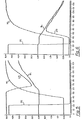
- Curve 22 intersects curve 20 at three points, 24a, 24b, and 24c.
- Points 24a and 24c are stable operating points and thus represent information stored in the memory cell; whereas point 24b is an unstable operating point.
- Information would be read from this modified memory cell by precharging the bit line to the voltage corresponding to point 24b, and thereafter turning on transistor 15.
- an improved static memory cell which includes first and second conductive means for carrying respective bias voltages in the cell, a third conductive means for carrying an input/output voltage signal in the cell, and a Lambda diode coupled between the first and third conductive means for there producing a negative dynamic resistance whenever the input/output voltage signal is within a predetermined range between the bias voltages on the first and second conductive means.
- a voltage dependent resistance means coupled between the second and third conductive means for there producing a negative dynamic resistance in response to at least some of the input/output voltages within said range.
- this voltage dependent resistance means is another Lambda diode which consists of either a pair of insulated gate field effect transistors or a pair of junction field effect transistors.
- This embodiment includes a pair of Lambda diodes 30 and 40 which are interconnected as illustrated.
- Symbol Q N1 indicates the N-channel depletion mode field effect transistor within Lambda diode 30; and symbol Q P1 indicates the P-channel depletion mode field effect transistor within Lambda diode 30.
- symbol Q N2 indicates the N-channel field effect transistor within Lambda diode 40; and symbol Q P2 indicates the P-channel depletion mode transistor within Lambda diode 40.
- One terminal 31 of Lambda diode 30 connects to a conductor 51 which carries a bias voltage V dd . That terminal 31 also interconnects the gate of transistor Q Pl and the drain of transistor Q N1 .
- Another conductor 52 which carries an input/output voltage signal to the memory cell connects to the other terminal 32 of Lambda diode 30. Terminal 32, in turn, interconnects the gate of transistor Q N1 and the drain of transistor Q P1 .
- One terminal 41 of Lambda diode 40 also connects to conductor 52. And terminal 41 in turn interconnects the gate of transistor Qp 2 with the drain of transistor QN2.
- the other terminal 42 of Lambda diode 40 connects to another conductor 53 which carries a ground bias voltage. Terminal 42 also interconnects the gate of transistor Q N2 and the drain of transistor Qp 2 .
- Memory cell by means of an enhancement mode N-channel transistor 54, a bit line 55, and a word line 56.
- the voltage on word line 56 is made high to turn transistor 54 on: and simultaneously, the voltage on bit line 55 is selectively made either relatively high or relatively low, depending upon the voltage that is desired to be written into the memory cell.
- bit line 55 is precharged to a voltage midway between the "high” and “low” voltage states of the memory cells. Then transistor 54 is turned on. And then the precharged voltage on bit line 55 either increases or decreases depending upon whether a "high” voltage or "low” voltage was stored in the memory cell.
- curves 30a and 40a which respectively indicate the I-V characteristics of Lambda diodes 30 and 40. That is, curve 30a shows the current through Lambda diode 30 as the voltage on terminal 32 changes from ground to the bias voltage V dd . Similarly, curve 40a shows the current through Lambda diode 40 as the voltage on terminal 41 changes from ground to the bias voltage V dd .
- curve 40a its shape is identical to the shape of the previously described curve 20 of Figure 2. So how the shape of curve 40a comes about needs no further explanation. But by comparison, curve 30a is shaped as the mirror image of curve 40a. This is explained as follows.
- bias voltage V dd and voltage V' V equals the magnitude of the threshold voltage of transistor Q N1 plus the magnitude of the threshold voltage of transistor Q Pl .
- diode 30 exhibits a negative dynamic resistance.
- diode 30 acts as a high resistance device which passes only a leakage current.
- curves 30a and 40a in Figure 4 show that those curves intersect each other at three points, 60a, 60b, and 60c.
- Points 60a and 60c are stable operating points; and thus the voltage at terminals 32 and 41 at those points represents information stored in the memory cell. That is, the voltage at point 60a is the "low” voltage state of the memory cell whereas the voltage at point 60c is the "high" voltage state of the memory cell.
- Point 60b by comparison, is an unstable operating point. Thus, it is not utilized to store information in the memory cell; but instead it is entered to read information from that cell. This read operation occurs as follows.
- bit line 55 is precharged to the voltage corresponding to point 60b. Thereafter, the voltage on word line 56 is raised to turn on transistor 54. Consequently, if a "high" voltage was stored on terminals 32 and 41, that voltage will drop to a voltage just to the right of the voltage at point 60b.
- curves 30a and 40a show that if the voltage at terminals 32 and 41 moves just slightly to the right of point 60b, then the current through Lambda diode 30 will be substantially greater than the current through Lambda diode 40. Thus, a large excess current will flow through transistor 54 to charge bit line 55.
- bit line 55 further increases the voltage at terminals 32 and 41; which further increases the difference between the respective currents through Lambda diodes 30 and 40.
- bit line 55 quickly charges to the "high" point 60c.
- curves 30a and 40a show that when the voltage on terminals 32 and 41 is just slightly to the left of point 60b, Lambda diode 40 sinks substantially more current than Lambda diode 30 supplies. And this large excess current which Lambda diode 40 sinks operates to quickly discharge bit line 55. So the voltage on bit line 55 quickly drops to the voltage at point 60a.
- bias voltage V dd there is an upper limit to bias voltage V dd .
- the upper limit equals the sum of the magnitude of the respective threshold voltages for transistors Q N1 ,Q P1 , Q N2' and Qp 2 .
- This constraint ensures that voltage V' V of curve 30a is less than voltage V v of curve 40a. In other words, it ensures that the respective voltage ranges in which Lambda diodes 30 and 40 exhibit their negative dynamic resistance overlap.
- the crossover point 60b occurs as illustrated.
- bias voltage V dd must be greater than the sum of the threshold voltages for transistors Q N1 and Q P1 ; and it must also be greater than the sum of the threshold voltages for transistors Q N2 and Qp 2 . This ensures that when the memory cell is in its "low” voltage state, the voltage drop across Lambda diode 30 will be sufficient to turn that diode completely off; and when the memory cell is in its "high” voltage state, the voltage drop across Lambda diode 40 will be sufficient to turn that diode completely off.
- each of the transistors Q N1' Q P1 , Q N2 , and Q P2 had minimum length/width geometries of 2.5 um/2.5 um. Also, transistors Q N1 and Q N2 each had a threshold voltage of +2 volts; while transistors Q P1 and Q P2 each had a threshold of -2 volts.
- bit line 55 was assumed to have a capacitance of 0.5 pf. This is about the capacitance one would expect in a memory chip containing 64,000 of the Figure 3 memory cells. Also, bias voltage V dd was set at 5 volts.
- time is plotted on the horizontal axis and voltage is plotted on the vertical axis.
- the number 10 indicates 10 nanoseconds
- the number 20 indicates 20 nanoseconds
- the number 1 indicates 1 volt
- the number 2 indicates 2 volts, etc.
- Each of the Figures 5 and 6 contains a set of four curves which are respectively labeled WL, BL, I/O, and PC.
- Curve WL indicates the voltage on word line 56;
- curve BL indicates the voltage on bit line 55; and
- curve I/O indicates the voltage on terminals 32, 41, and conductor 52.
- the remaining curve PC indicates the gate voltage on a transistor (not shown) which is utilized to connect a precharge voltage to the bit line.
- bit line is precharged to 2.5 volts. Thereafter, signal PC goes low to isolate the precharging voltage source from the bit line. And then at a time of about 40 nanoseconds, the word line voltage WL goes high to turn on transistor 54.
- both the bit line voltage and the "low" voltage state that was stored in the memory cell move toward each other. Then, since Lambda diode 40 sinks more current than Lambda diode 30 supplies, both the bit line voltage and the 1/0 voltage decrease toward 0 volts.
Landscapes
- Engineering & Computer Science (AREA)
- Computer Hardware Design (AREA)
- Semiconductor Memories (AREA)
- Static Random-Access Memory (AREA)
- Solid State Image Pick-Up Elements (AREA)
Applications Claiming Priority (2)
| Application Number | Priority Date | Filing Date | Title |
|---|---|---|---|
| US307158 | 1981-09-30 | ||
| US06/307,158 US4376986A (en) | 1981-09-30 | 1981-09-30 | Double Lambda diode memory cell |
Publications (2)
| Publication Number | Publication Date |
|---|---|
| EP0076139A2 true EP0076139A2 (fr) | 1983-04-06 |
| EP0076139A3 EP0076139A3 (fr) | 1985-10-16 |
Family
ID=23188501
Family Applications (1)
| Application Number | Title | Priority Date | Filing Date |
|---|---|---|---|
| EP82305098A Withdrawn EP0076139A3 (fr) | 1981-09-30 | 1982-09-28 | Cellule de mémoire à double diode lambda |
Country Status (4)
| Country | Link |
|---|---|
| US (1) | US4376986A (fr) |
| EP (1) | EP0076139A3 (fr) |
| JP (1) | JPS58501607A (fr) |
| WO (1) | WO1983001335A1 (fr) |
Families Citing this family (5)
| Publication number | Priority date | Publication date | Assignee | Title |
|---|---|---|---|---|
| JPH04155693A (ja) * | 1990-10-18 | 1992-05-28 | Nec Ic Microcomput Syst Ltd | 半導体記憶装置のデータ出力回路 |
| JP3397516B2 (ja) * | 1995-06-08 | 2003-04-14 | 三菱電機株式会社 | 半導体記憶装置及び半導体集積回路装置 |
| US10205313B2 (en) | 2015-07-24 | 2019-02-12 | Symptote Technologies, LLC | Two-transistor devices for protecting circuits from sustained overcurrent |
| CN108292837B (zh) | 2015-09-21 | 2020-01-17 | 西普托特技术有限责任公司 | 用于保护电路的单晶体管器件以及方法 |
| US12614575B1 (en) * | 2023-09-07 | 2026-04-28 | Synopsys, Inc. | Half static random access memory (SRAM) cell |
Family Cites Families (5)
| Publication number | Priority date | Publication date | Assignee | Title |
|---|---|---|---|---|
| NL261224A (fr) * | 1960-02-15 | |||
| JPS5176945A (ja) * | 1974-12-27 | 1976-07-03 | Nippon Electric Co | Esakidaioodohikakuki |
| US4053798A (en) * | 1975-02-20 | 1977-10-11 | Matsushita Electronics Corporation | Negative resistance device |
| JPS52153630A (en) * | 1976-06-16 | 1977-12-20 | Matsushita Electric Ind Co Ltd | Semiconductor memory device |
| DE2916884C3 (de) * | 1979-04-26 | 1981-12-10 | Deutsche Itt Industries Gmbh, 7800 Freiburg | Programmierbare Halbleiterspeicherzelle |
-
1981
- 1981-09-30 US US06/307,158 patent/US4376986A/en not_active Expired - Lifetime
-
1982
- 1982-09-24 WO PCT/US1982/001327 patent/WO1983001335A1/fr not_active Ceased
- 1982-09-24 JP JP57503196A patent/JPS58501607A/ja active Pending
- 1982-09-28 EP EP82305098A patent/EP0076139A3/fr not_active Withdrawn
Also Published As
| Publication number | Publication date |
|---|---|
| WO1983001335A1 (fr) | 1983-04-14 |
| EP0076139A3 (fr) | 1985-10-16 |
| US4376986A (en) | 1983-03-15 |
| JPS58501607A (ja) | 1983-09-22 |
Similar Documents
| Publication | Publication Date | Title |
|---|---|---|
| US6469929B1 (en) | Structure and method for high speed sensing of memory arrays | |
| US4648074A (en) | Reference circuit with semiconductor memory array | |
| KR970006622B1 (ko) | 기준전압을 소정레벨에 클램핑 하는 클램프 회로 | |
| US4409496A (en) | MOS Device including a substrate bias generating circuit | |
| EP0643393A2 (fr) | Dispositif de mémoire à semi-conducteurs avec circuit élévateur de tension | |
| KR0155078B1 (ko) | 강전계용의 mos 회로를 갖춘 반도체 회로 | |
| US5859798A (en) | Read circuit for non-volatile memory working with a low supply voltage | |
| KR20020020266A (ko) | 강유전체 메모리 | |
| KR0140025B1 (ko) | 반도체 기억 장치 | |
| US3969708A (en) | Static four device memory cell | |
| EP0050529A2 (fr) | Circuit de mémoire semiconductrice | |
| EP0154547B1 (fr) | Mémoire dynamique écriture-lecture à accès aléatoire | |
| US6600672B2 (en) | Semiconductor memory device | |
| US4578781A (en) | MIS transistor circuit | |
| US6628162B2 (en) | Semiconductor integrated circuit | |
| US6404666B1 (en) | Read only memory having correction current supplying circuit | |
| US9558792B2 (en) | Voltage generating circuit | |
| US6198681B1 (en) | Sense amplifier for low voltage memory arrays | |
| KR19980064537A (ko) | 반도체 기억장치 | |
| US4376986A (en) | Double Lambda diode memory cell | |
| KR100409186B1 (ko) | 기록및독출에서독립적으로제어되는메모리셀회로 | |
| EP1324344B1 (fr) | Structure d'amplificateur de lecture pour des dispositifs de mémoire multibit et méthode de lecture associée | |
| US5199000A (en) | Semiconductor memory circuit having switched voltage supply for data bus lines | |
| US5623440A (en) | Multiple-bit random access memory cell | |
| KR102481452B1 (ko) | 강유전체 소자 기반 nor 타입 내용 주소화 메모리 셀 및 이를 포함하는 내용 주소화 메모리 |
Legal Events
| Date | Code | Title | Description |
|---|---|---|---|
| PUAI | Public reference made under article 153(3) epc to a published international application that has entered the european phase |
Free format text: ORIGINAL CODE: 0009012 |
|
| 17P | Request for examination filed |
Effective date: 19821002 |
|
| AK | Designated contracting states |
Designated state(s): BE DE FR GB IT NL SE |
|
| PUAL | Search report despatched |
Free format text: ORIGINAL CODE: 0009013 |
|
| AK | Designated contracting states |
Designated state(s): BE DE FR GB IT NL SE |
|
| RAP1 | Party data changed (applicant data changed or rights of an application transferred) |
Owner name: BURROUGHS CORPORATION (A DELAWARE CORPORATION) |
|
| 17Q | First examination report despatched |
Effective date: 19861125 |
|
| RAP1 | Party data changed (applicant data changed or rights of an application transferred) |
Owner name: UNISYS CORPORATION |
|
| STAA | Information on the status of an ep patent application or granted ep patent |
Free format text: STATUS: THE APPLICATION IS DEEMED TO BE WITHDRAWN |
|
| 18D | Application deemed to be withdrawn |
Effective date: 19880811 |
|
| RIN1 | Information on inventor provided before grant (corrected) |
Inventor name: ELMASRY, MOHAMED IBRAHIM Inventor name: PETERSON, LUVERNE RAY |