EP0076617A2 - Process and apparatus for identifying coins - Google Patents
Process and apparatus for identifying coins Download PDFInfo
- Publication number
- EP0076617A2 EP0076617A2 EP82305086A EP82305086A EP0076617A2 EP 0076617 A2 EP0076617 A2 EP 0076617A2 EP 82305086 A EP82305086 A EP 82305086A EP 82305086 A EP82305086 A EP 82305086A EP 0076617 A2 EP0076617 A2 EP 0076617A2
- Authority
- EP
- European Patent Office
- Prior art keywords
- magnetic field
- detector
- standard
- coin
- alternating magnetic
- Prior art date
- Legal status (The legal status is an assumption and is not a legal conclusion. Google has not performed a legal analysis and makes no representation as to the accuracy of the status listed.)
- Granted
Links
- 238000000034 method Methods 0.000 title claims abstract description 20
- 230000008569 process Effects 0.000 title claims abstract description 18
- 230000005291 magnetic effect Effects 0.000 claims abstract description 61
- 239000000463 material Substances 0.000 claims abstract description 37
- 239000004020 conductor Substances 0.000 claims abstract description 28
- 239000013078 crystal Substances 0.000 claims abstract description 14
- 230000008859 change Effects 0.000 claims description 29
- 238000012360 testing method Methods 0.000 claims description 17
- 230000004044 response Effects 0.000 claims 3
- 239000002184 metal Substances 0.000 description 8
- 229910052751 metal Inorganic materials 0.000 description 8
- 230000006870 function Effects 0.000 description 5
- 230000008901 benefit Effects 0.000 description 4
- 230000000694 effects Effects 0.000 description 4
- 229910045601 alloy Inorganic materials 0.000 description 3
- 239000000956 alloy Substances 0.000 description 3
- 238000001514 detection method Methods 0.000 description 3
- 150000002739 metals Chemical class 0.000 description 3
- 230000004048 modification Effects 0.000 description 3
- 238000012986 modification Methods 0.000 description 3
- 239000010409 thin film Substances 0.000 description 3
- 239000010408 film Substances 0.000 description 2
- 238000005259 measurement Methods 0.000 description 2
- 238000012544 monitoring process Methods 0.000 description 2
- 238000005096 rolling process Methods 0.000 description 2
- 229910000906 Bronze Inorganic materials 0.000 description 1
- RYGMFSIKBFXOCR-UHFFFAOYSA-N Copper Chemical compound [Cu] RYGMFSIKBFXOCR-UHFFFAOYSA-N 0.000 description 1
- 229910000570 Cupronickel Inorganic materials 0.000 description 1
- 239000010974 bronze Substances 0.000 description 1
- 229910052802 copper Inorganic materials 0.000 description 1
- 239000010949 copper Substances 0.000 description 1
- KUNSUQLRTQLHQQ-UHFFFAOYSA-N copper tin Chemical compound [Cu].[Sn] KUNSUQLRTQLHQQ-UHFFFAOYSA-N 0.000 description 1
- 230000003247 decreasing effect Effects 0.000 description 1
- 239000003302 ferromagnetic material Substances 0.000 description 1
- 230000006698 induction Effects 0.000 description 1
- 230000007246 mechanism Effects 0.000 description 1
- 230000000737 periodic effect Effects 0.000 description 1
- 230000035699 permeability Effects 0.000 description 1
- 230000008672 reprogramming Effects 0.000 description 1
Images


Classifications
-
- G—PHYSICS
- G07—CHECKING-DEVICES
- G07D—HANDLING OF COINS OR VALUABLE PAPERS, e.g. TESTING, SORTING BY DENOMINATIONS, COUNTING, DISPENSING, CHANGING OR DEPOSITING
- G07D5/00—Testing specially adapted to determine the identity or genuineness of coins, e.g. for segregating coins which are unacceptable or alien to a currency
- G07D5/08—Testing the magnetic or electric properties
-
- G—PHYSICS
- G07—CHECKING-DEVICES
- G07D—HANDLING OF COINS OR VALUABLE PAPERS, e.g. TESTING, SORTING BY DENOMINATIONS, COUNTING, DISPENSING, CHANGING OR DEPOSITING
- G07D5/00—Testing specially adapted to determine the identity or genuineness of coins, e.g. for segregating coins which are unacceptable or alien to a currency
- G07D5/02—Testing the dimensions, e.g. thickness, diameter; Testing the deformation
Definitions
- This invention relates to a process and apparatus particularly suitable for detecting, identifying, classifying and locating electrically conducting material.
- the process and apparatus are particularly suitable for identifying coins.
- Inductance techniques have been used for this purpose, such techniques being based on the change in inductance of a coil when a coin is introduced into close proximity. However, such systems detect only the overall effect of the coin as a whole.
- the present invention makes use of other detectors which, when an alternating magnetic field is applied to electrically conducting material, can detect.local changes in the magnetic field over selected areas of the electrically conducting materials.
- alternating includes any periodic change about a base line without necessarily involving a change in polarity of the field, i.e. it also includes a field which alternates between increasing and decreasing field strength without involving a change of direction of the field.
- the magnetoresistive effect in thin films of certain ferromagnetic material arises from an anisotropic contribution ⁇ , to the total resistitivy ⁇ .
- Hunt has analysed this effect (Transactions of Institute of Electrical and Electronic Engineer, Mag.7 (1971) pp 150-4) and has shown that the change in resistivity of an element of a film or thin sheet of the material, and hence the change in terminal voltage if a constant current is passed along the element, is a function of a magnetic field or the component thereof applied to the element in the plane of the film. Consequently, the detector can be thin and so very selective.
- Hall crystal When a Hall crystal is used to detect the local magnetic field applied to it, the field gives rise to an output voltage from the crystal. They can be used to product detectors which are substantially rectangular or square, the voltage generated being a function of the magnetic field or the component thereof normal to the plane of the crystal.
- magnetoresistive or Hall crystal detectors are applied to the detection of local changes in an alternating magnetic field which arise when an electrically conducting material is placed in the field, the resulting change in the electrical characteristics of the detector being used for example to identify, classify or locate the conducting material.
- the invention also provides apparatus for identifying, classifying or locating an electrically conducting material comprising means for applying an alternating magnetic field to the material and a magnetoresistive or Hall crystal detector arranged to detect local changes in the magnetic field resulting from the presence therein of the material.
- the invention is based on the fact that when an electrically conducting material is placed in a changing applied magnetic field, eddy currents are induced in the material which currents modify the local field in close proximity to the material.
- the nature of the modification over any particular area of the material will depend on such factors as the nature of the material and its dimension and may vary from area to area.
- the electrical signal thus produced by a magnetoresistor or a Hall crystal can readily be compared with a standard or a reference value and any differences or similarities between them can readily be determined by conventional means and the resulting determination can be used for identification, classification or location of the electrically conducting material.
- the change in the magnetic field in the vicinity of the material resulting from the induced eddy currents in the electrically conducting material is both in amplitude and in phase relative to the applied field or to a reference field and the above-mentioned detectors may be used to detect one or the other of these parameters and produce an appropriate signal.
- comparison may be made with a standard detector of the same type positioned within the applied magnetic field but outside the locality in which the change in magnetic field occurs.
- the voltage across the detector in the locality of the changed field is compared with the voltage across the standard detector and the change in voltage provides a measure of the local change in amplitude of the magnetic field.
- phase standard for comparison When measuring changes in phase of the local magnetic field the phase standard for comparison can be taken from the drive to the applied magnetic field or a reference field.
- This embodiment of the invention has the advantage that problems of drift, which may be present in amplitude detection systems, can be much reduced or even eliminated.
- the changed field resulting from placing a test sample of the material in it as compared with a reference field as changed by a standard sample of the material.
- the material is a coin
- a null difference between the fields when compared at one or more corresponding points on the two coins indicates that they are of the same type.
- a significant difference at one or more pairs of corresponding points indicates that the coins are dissimilar. Measurements at several different pairs of points across the two coins makes the comparison much more sensitive and reliable.
- the applied magnetic field is preferably a regularly alternating magnetic field and the most suitable frequency of such an alternating magnetic field applied to the electrically conducting material depends to some extent on the nature of the material.
- a frequency of 2 to 6 kH 2 , or preferably 3 to 5 kH z is particularly suitable for cupro- nickel coins.
- a frequency of 0.5 to 2 kH z , or preferably of 0.75 to 1.5 kH z is particuarly suitable.
- a first frequency say about 2 kH z
- a further frequency or frequencies most suitable for that alloy then being applied to further identify the coin, e.g. by dimensions.
- An advantage arising from the detectors used in the present invention is that they can be m ade very small, for example,from 5 mm to 1 mm in length and/or width, and in consequence can detect changes in magnetic fields over equivalently small areas. They can therefore be used to survey in much finer detail than say when using a larger conventional induction coil. They are particularly useful in locating an edge of the conducting material since there is a marked change in the local magnetic field at this point and because of the small thickness of the detector, say 400 ⁇ the edge can be located with a high degree of accuracy, possibly to as little as ⁇ 0.5 micro m. In this way, for example, the diameter of a coin may be identified, or the edge of a running strip of metal located.
- an array of detectors may be used in conjunction with an electronic multiplexing system to provide a simultaneous detailed survey of changes in local magnetic field.
- the array may be linear to provide a simultaneous survey.say across a whole diameter of a coin, or the multiplicity of detectors may be so spaced as to be capable of surveying-an area simultaneously.
- the detector output is a function of, inter alia:
- FIG.l An example of the changes in output of a magnetoresistor detector, when placed in an alternating magnetic field in close proximity to a coin, is shown in Fig.l.
- the figure shows the relative change in output (compared to the case with no coin present) as a function of frequency for various coins. These results were obtained with the detector perpendicular to the coin, and in intimate contact with the centre of the coin.
- the applied field was a uniform sinusoidal field applied perpendicular to the coin.
- the experimental arrangement is shown in Fig.2. in which a thin-film magnetoresistive detector 1 is positioned adjacent the centre of a coin 2 which is subjected to an alternating magnetic field H.
- the detector is 2 mm long, 300 A thick and 50 mm high.
- a constant current is passed through the detector, the leads also being used in measuring the change in voltage across the detector.
- the change in voltage is then compared against a standard provided by a similar magnetoresistor 4 with leads 5 which is located within the uniform applied field but outside the locality affected by eddy currents in the coin 2.
- the standard resistor was 10 mm away from the detector.
- the signals from the two magnetoresistors are amplified and filtered and then fed into a differential amplifier, the output from which is proportional to the local change in field due to eddy currents. The results show that by employing one or more applied field frequencies it is possible to discriminate between coins.
- Figure 3 shows the relative change in output of the detector as a function of the position of the detector on a line drawn through the diameter of two different coins.
- a single detector as employed in this case
- an array of detectors can be employed to discriminate between coins of different alloys, diameter and/or shape, i.e. by monitoring the output of detector(s) when placed at different points on the coin.
- the sharp upturn at the ends of the curves indicates the edge of the coin and it will be noted that these coincide quite closely with the ends of the indicated actual diameters of the coins.
- the detectors may thus be employed to discriminate between coins of different materials and size. Further, some difference in surface profiles can be employed to discriminate between different coins.
- a secure coin identification system based on either a single detector or an array of detectors.
- the system can be employed to discriminate between coins of a particular country and/or between coinage from different countries.
- the system can be made compatible with microprocessor-based vending machines including those dispensing change. All signals are electrical in nature at source. Since the identification can be carried out statically or dynamically, i. e. with the coin stationary or moving, the present invention can readily be applied to coin operated machines.
- FIG.4 An application of this invention using standard samples is illustrated in Fig.4 in which a test coin 1 and a standard sample coin 2 are located in an alternating magnetic field generated by coils 3 and 4 driven by identical drives.
- Magnetoresistor detectors 5 and 6 are provided adjacent each coin with facilities (not shown) for positioning the detectors synchronously at predetermined points on the coins.
- the signals generated by the resistors i.e. the voltage across the detectors when a constant current is passed through them, are amplified in amplifiers 7 and 8 and any phase difference between the signals is compared in phase difference circuit 9.
- the output is passed through a digital filter 10 which eliminates false pulses due to noise, the filter being adjusted by a tolerance control 11.
- the filtered output is then used to operate an accept/reject control 12. If the phase difference is significant the test coin is rejected.
- the detector 6 is fixed in relation to the standard sample coin 2, say at the centre of the coin.
- Detector 5 is located in a slide which conveys the test coin 1 and a reading of its output signal is taken at the moment when its position in relation to the test coin 1 is the same as that of detector 6 in relation to coin 2.. Again, if there is a null or acceptable difference between the signals from the two detectors, the test coin is accepted. If.there is a significant difference it is rejected.
- the process and apparatus of this invention can be applied to electrically conducting material where size, for example thickness, is to be classified. Such size classification can be applied to monitoring the size of material being produced.
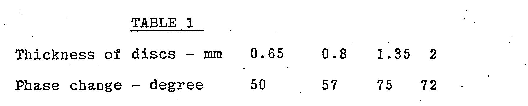
- Table 1 shows the results of measuring at the centre of copper discs of 2.6 mm diameter, the phase change of an alternating sinusoidal magnetic field of 2 kH z frequency applied perpendicularly to the discs.
- a Hall crystal detector approximately 2.5 mm square placed in the centre of the discs was used to detect the change in phase with reference to the drive to the applied magnetic field.
- the change in phase with any particular thickness varies with the frequency of the applied field.
- the most suitable frequency to use will therefore depend on the range of thicknesses to be measured and also on the other dimensions of the electrically conducting material to be checked, and on the nature of the material.
- the optimum frequency in any particular circumstances can readily be established by preliminary tests.
- the output from a detector of this invention used to detect change in thickness can be applied for example to control the thickness of metal strip or sheet produced by a rolling mill.
- the magnitude of the eddy currents generated in conductive material subjected to the alternating magnetic field, and consequently the local changes in the magnetic field, depends on the nature of the material and in another application of this invention the process and apparatus is used to identify different metals.
- Table 2 shows the results of measuring, by means of a magnetoresistor detector, the change in phase of an alternating magnetic field of 1 kH z frequency at the centre of discs of the same size but of different metals to which the alternating field was applied, the phase change being with reference to the drive of the magnetic field.
- T he discs were 2.6 mm diameter and 2 mm thick.
- the process and apparatus of this invention may also be used to locate the position of metals, particularly the edges of metal sheet, and another application is in guiding metal strip through, for example, a rolling mill.
- the detector is located over an edge of the strip, preferably one detector over each opposed edge of the strip.
- the signal from the detectors may be compared with a standard reference value or with the signal from a standard detector positioned over the centre of the strip. A sideways drift of the metal strip produces an imbalance between the signals which is used to control the direction of the strip to centre it again.
- the process and apparatus of this invention may be used to classify electrically conducting material by detecting cracks, flaws or discont'inuites in it.
- the surface of the material is-scanned by a magnetic field generator and two detectors spaced apart.
- the spaced detectors normally produce identical signals which when compared produce a null result.
- an imbalance of-the signal occurs and is used to operate a warning indicator.
Landscapes
- Physics & Mathematics (AREA)
- General Physics & Mathematics (AREA)
- Testing Of Coins (AREA)
- Investigating Or Analyzing Materials By The Use Of Magnetic Means (AREA)
- Crystals, And After-Treatments Of Crystals (AREA)
Abstract
Description
- This invention relates to a process and apparatus particularly suitable for detecting, identifying, classifying and locating electrically conducting material. The process and apparatus are particularly suitable for identifying coins.
- Since the advent of coin-operated mechanisms many different detector systems have been employed for discriminating between the materials and/or sizes of coins. Inductance techniques have been used for this purpose, such techniques being based on the change in inductance of a coil when a coin is introduced into close proximity. However, such systems detect only the overall effect of the coin as a whole.
- The present invention makes use of other detectors which, when an alternating magnetic field is applied to electrically conducting material, can detect.local changes in the magnetic field over selected areas of the electrically conducting materials. The term "alternating" includes any periodic change about a base line without necessarily involving a change in polarity of the field, i.e. it also includes a field which alternates between increasing and decreasing field strength without involving a change of direction of the field.
- The magnetoresistive effect in thin films of certain ferromagnetic material arises from an anisotropic contributionΔρ, to the total resistitivy ρ. Hunt has analysed this effect (Transactions of Institute of Electrical and Electronic Engineer, Mag.7 (1971) pp 150-4) and has shown that the change in resistivity of an element of a film or thin sheet of the material, and hence the change in terminal voltage if a constant current is passed along the element, is a function of a magnetic field or the component thereof applied to the element in the plane of the film. Consequently, the detector can be thin and so very selective.
- When a Hall crystal is used to detect the local magnetic field applied to it, the field gives rise to an output voltage from the crystal. They can be used to product detectors which are substantially rectangular or square, the voltage generated being a function of the magnetic field or the component thereof normal to the plane of the crystal.
- Both detectors can be made small with the advantage described Lter.
- According to this invention, magnetoresistive or Hall crystal detectors, are applied to the detection of local changes in an alternating magnetic field which arise when an electrically conducting material is placed in the field, the resulting change in the electrical characteristics of the detector being used for example to identify, classify or locate the conducting material.
- The invention also provides apparatus for identifying, classifying or locating an electrically conducting material comprising means for applying an alternating magnetic field to the material and a magnetoresistive or Hall crystal detector arranged to detect local changes in the magnetic field resulting from the presence therein of the material.
- The invention is based on the fact that when an electrically conducting material is placed in a changing applied magnetic field, eddy currents are induced in the material which currents modify the local field in close proximity to the material. The nature of the modification over any particular area of the material will depend on such factors as the nature of the material and its dimension and may vary from area to area.
- We have found that in the case of a coin the local modification of the applied field varies from a point just outside one end of the coin to a point just outside the opposite edge of the coin and that, for example, a profile of these variations across a diameter of the coin can be prepared from a multiplicity of measurements across the coin using a detector comprising a magnetoresistor or Hall crystal.
- These modifications in the field can be detected using thin film magnetoresistors, the resistance of which changes when a magnetic field is applied thereto. The change in resistance resulting from a change in the applied magnetic field can be detected and in known manner can be used, to identify, and optionally reject or accept, to classify or to locate the electrically conductive material present in the field. Usually, a constant current is passed through the magnetoresistor and the different resistance due to the different characteristics of that part of the field in which it is located is evidenced by a different voltage over the terminals of the resistor.
- Similarly, when a Hall crystal is used as the detector, a difference in the magnetic field in the vicinity of the- material give rise to a difference in the output voltage of the crystal.
- The electrical signal thus produced by a magnetoresistor or a Hall crystal can readily be compared with a standard or a reference value and any differences or similarities between them can readily be determined by conventional means and the resulting determination can be used for identification, classification or location of the electrically conducting material.
- The change in the magnetic field in the vicinity of the material resulting from the induced eddy currents in the electrically conducting material is both in amplitude and in phase relative to the applied field or to a reference field and the above-mentioned detectors may be used to detect one or the other of these parameters and produce an appropriate signal.
- When measuring changes in amplitude of the local magnetic field comparison may be made with a standard detector of the same type positioned within the applied magnetic field but outside the locality in which the change in magnetic field occurs. The voltage across the detector in the locality of the changed field is compared with the voltage across the standard detector and the change in voltage provides a measure of the local change in amplitude of the magnetic field.
- When measuring changes in phase of the local magnetic field the phase standard for comparison can be taken from the drive to the applied magnetic field or a reference field. This embodiment of the invention has the advantage that problems of drift, which may be present in amplitude detection systems, can be much reduced or even eliminated.
- In another embodiment of the invention which is particularly suitable for identifying coins, the changed field resulting from placing a test sample of the material in it as compared with a reference field as changed by a standard sample of the material. When the material is a coin a null difference between the fields when compared at one or more corresponding points on the two coins, indicates that they are of the same type. On the other hand, a significant difference at one or more pairs of corresponding points indicates that the coins are dissimilar. Measurements at several different pairs of points across the two coins makes the comparison much more sensitive and reliable.
- Advantages of this embodiment using standard samples are:
- 1. the applied magnetic field need not be so accurately controlled since changes in the field would affect both coins.
- 2. a memory unit which otherwise may be needed to provide standard reference values for comparison will not be required.
- 3. simpler electronic circuitry may be used.
- 4. the detection unit may be-less sensitive to the effects of external magnetic fields or variations in voltage supply.
- 5. reprogramming of the process or apparatus for a different standard or set of standards, is simply effected by changing the standard sample or samples. In multiple coin detector units for example, sample coins of the acceptable types may be located in a sample block and an inserted coin may be compared sequentially with each standard sample coin in the block until a true comparison is encountered, failing which the inserted coin is rejected.
- The applied magnetic field is preferably a regularly alternating magnetic field and the most suitable frequency of such an alternating magnetic field applied to the electrically conducting material depends to some extent on the nature of the material. For example, when this invention is used in identification, followed by acceptance or rejection, of coins a frequency of 2 to 6 kH2, or preferably 3 to 5 kHz, is particularly suitable for cupro- nickel coins. When applied to bronze coins, a frequency of 0.5 to 2 kHz, or preferably of 0.75 to 1.5 kHz, is particuarly suitable.
- In identifying coins, a first frequency, say about 2 kHz, may be applied in order to identify the alloy of the coin, a further frequency or frequencies most suitable for that alloy then being applied to further identify the coin, e.g. by dimensions.
- An advantage arising from the detectors used in the present invention is that they can be m ade very small, for example,from 5 mm to 1 mm in length and/or width, and in consequence can detect changes in magnetic fields over equivalently small areas. They can therefore be used to survey in much finer detail than say when using a larger conventional induction coil. They are particularly useful in locating an edge of the conducting material since there is a marked change in the local magnetic field at this point and because of the small thickness of the detector, say 400Å the edge can be located with a high degree of accuracy, possibly to as little as ± 0.5 micro m. In this way, for example, the diameter of a coin may be identified, or the edge of a running strip of metal located.
- Instead of a single detector, an array of detectors may be used in conjunction with an electronic multiplexing system to provide a simultaneous detailed survey of changes in local magnetic field. The array may be linear to provide a simultaneous survey.say across a whole diameter of a coin, or the multiplicity of detectors may be so spaced as to be capable of surveying-an area simultaneously.
- The detector output is a function of, inter alia:
- 1. ' The frequency and form of the applied field.
- 2. The amplitude and orientation of the applied field.
- 3. The dimensions of the conducting material.
- 4. The conductivity/resistivity permeability of the material.
- 5. The shape of the material.
- 6. The surface profile of the material.
- 7. The presence or absence, in the vicinity of the detector, of a conducting material.
- 8. The orientation and position of the detector relative to the conducting material and applied field.
- 9. The material, dimensions and current density employed in the detector.
- In the accompanying drawings the use of a magnetoresistor detector is illustrated by way of example in Figs. 1 - 3 of the accompanying drawings in which:
- Fig. 1 shows the changes in amplified (x 1000) output voltage of an unbiased magnetoresistor. detector when placed in a uniform alternating applied field, in close proximity to the centre of various coins.
- Fig. 2 shows the experimental arrangement employed to obtain the results shown in Fig.l
- Fig. 3 shows the relative changes in output of a magnetoresistor detector as it is traversed across the diameter of two different coins.
- The use of a standard sample for comparison is illustrated by way of example in Fig.4.
- An example of the changes in output of a magnetoresistor detector, when placed in an alternating magnetic field in close proximity to a coin, is shown in Fig.l. The figure shows the relative change in output (compared to the case with no coin present) as a function of frequency for various coins. These results were obtained with the detector perpendicular to the coin, and in intimate contact with the centre of the coin. The applied field was a uniform sinusoidal field applied perpendicular to the coin. The experimental arrangement is shown in Fig.2. in which a thin-film magnetoresistive detector 1 is positioned adjacent the centre of a
coin 2 which is subjected to an alternating magnetic field H. The detector is 2 mm long, 300 A thick and 50 mm high. Through leads 3 a constant current is passed through the detector, the leads also being used in measuring the change in voltage across the detector. The change in voltage is then compared against a standard provided by asimilar magnetoresistor 4 withleads 5 which is located within the uniform applied field but outside the locality affected by eddy currents in thecoin 2. In this case the standard resistor was 10 mm away from the detector. The signals from the two magnetoresistors are amplified and filtered and then fed into a differential amplifier, the output from which is proportional to the local change in field due to eddy currents. The results show that by employing one or more applied field frequencies it is possible to discriminate between coins. - Figure 3 shows the relative change in output of the detector as a function of the position of the detector on a line drawn through the diameter of two different coins. The results show that a single detector (as employed in this case) or an array of detectors can be employed to discriminate between coins of different alloys, diameter and/or shape, i.e. by monitoring the output of detector(s) when placed at different points on the coin. In Fig.3, the sharp upturn at the ends of the curves indicates the edge of the coin and it will be noted that these coincide quite closely with the ends of the indicated actual diameters of the coins.
- These parameters of constitution, size and shape can be determined with the coin stationary in or moving through the applied magnetic field.
- Similar results are obtained when the detector used is a Hall crystal.
- In the application of the process and apparatus of this invention to coin identification, the detectors may thus be employed to discriminate between coins of different materials and size. Further, some difference in surface profiles can be employed to discriminate between different coins. By storing this information by way of reference values for example in a microprocessor system, it is possible to provide a secure coin identification system based on either a single detector or an array of detectors. The system can be employed to discriminate between coins of a particular country and/or between coinage from different countries. The system can be made compatible with microprocessor-based vending machines including those dispensing change. All signals are electrical in nature at source. Since the identification can be carried out statically or dynamically, i. e. with the coin stationary or moving, the present invention can readily be applied to coin operated machines.
- An application of this invention using standard samples is illustrated in Fig.4 in which a test coin 1 and a
standard sample coin 2 are located in an alternating magnetic field generated bycoils Magnetoresistor detectors amplifiers 7 and 8 and any phase difference between the signals is compared inphase difference circuit 9. The output is passed through adigital filter 10 which eliminates false pulses due to noise, the filter being adjusted by atolerance control 11. The filtered output is then used to operate an accept/reject control 12. If the phase difference is significant the test coin is rejected. - In another embodiment where a lower degree of discrimination may be acceptable the
detector 6 is fixed in relation to thestandard sample coin 2, say at the centre of the coin.Detector 5 is located in a slide which conveys the test coin 1 and a reading of its output signal is taken at the moment when its position in relation to the test coin 1 is the same as that ofdetector 6 in relation to coin 2.. Again, if there is a null or acceptable difference between the signals from the two detectors, the test coin is accepted. If.there is a significant difference it is rejected. - The process and apparatus of this invention can be applied to electrically conducting material where size, for example thickness, is to be classified. Such size classification can be applied to monitoring the size of material being produced.
- Table 1 shows the results of measuring at the centre of copper discs of 2.6 mm diameter, the phase change of an alternating sinusoidal magnetic field of 2 kHz frequency applied perpendicularly to the discs. A Hall crystal detector approximately 2.5 mm square placed in the centre of the discs was used to detect the change in phase with reference to the drive to the applied magnetic field.
- The change in phase with any particular thickness varies with the frequency of the applied field. The most suitable frequency to use will therefore depend on the range of thicknesses to be measured and also on the other dimensions of the electrically conducting material to be checked, and on the nature of the material. The optimum frequency in any particular circumstances can readily be established by preliminary tests. The output from a detector of this invention used to detect change in thickness can be applied for example to control the thickness of metal strip or sheet produced by a rolling mill.
- The magnitude of the eddy currents generated in conductive material subjected to the alternating magnetic field, and consequently the local changes in the magnetic field, depends on the nature of the material and in another application of this invention the process and apparatus is used to identify different metals.
- Table 2 shows the results of measuring, by means of a magnetoresistor detector, the change in phase of an alternating magnetic field of 1 kHz frequency at the centre of discs of the same size but of different metals to which the alternating field was applied, the phase change being with reference to the drive of the magnetic field. T he discs were 2.6 mm diameter and 2 mm thick.

- The process and apparatus of this invention may also be used to locate the position of metals, particularly the edges of metal sheet, and another application is in guiding metal strip through, for example, a rolling mill. In this application, the detector is located over an edge of the strip, preferably one detector over each opposed edge of the strip. The signal from the detectors may be compared with a standard reference value or with the signal from a standard detector positioned over the centre of the strip. A sideways drift of the metal strip produces an imbalance between the signals which is used to control the direction of the strip to centre it again.
- Further, because of the possibility of detecting the change in magnetic field at a discontinuity in a conductor, the process and apparatus of this invention may be used to classify electrically conducting material by detecting cracks, flaws or discont'inuites in it. In this case, the surface of the material is-scanned by a magnetic field generator and two detectors spaced apart. The spaced detectors normally produce identical signals which when compared produce a null result. When one detector encounters a crack, flaw or discontinuity an imbalance of-the signal occurs and is used to operate a warning indicator.
Claims (16)
means for comparing the electrical signal generated by the standard detector in response to the magnetic field to which it is subjected with the signal generated by the test detector.
Priority Applications (1)
| Application Number | Priority Date | Filing Date | Title |
|---|---|---|---|
| AT82305086T ATE41070T1 (en) | 1981-10-02 | 1982-09-27 | METHOD AND EQUIPMENT FOR IDENTIFICATION OF COINS. |
Applications Claiming Priority (2)
| Application Number | Priority Date | Filing Date | Title |
|---|---|---|---|
| GB8129871 | 1981-10-02 | ||
| GB8129871 | 1981-10-02 |
Publications (3)
| Publication Number | Publication Date |
|---|---|
| EP0076617A2 true EP0076617A2 (en) | 1983-04-13 |
| EP0076617A3 EP0076617A3 (en) | 1983-09-14 |
| EP0076617B1 EP0076617B1 (en) | 1989-03-01 |
Family
ID=10524925
Family Applications (1)
| Application Number | Title | Priority Date | Filing Date |
|---|---|---|---|
| EP82305086A Expired EP0076617B1 (en) | 1981-10-02 | 1982-09-27 | Process and apparatus for identifying coins |
Country Status (6)
| Country | Link |
|---|---|
| US (1) | US4870360A (en) |
| EP (1) | EP0076617B1 (en) |
| JP (1) | JPS5886452A (en) |
| AT (1) | ATE41070T1 (en) |
| CA (1) | CA1228134A (en) |
| DE (1) | DE3279488D1 (en) |
Cited By (5)
| Publication number | Priority date | Publication date | Assignee | Title |
|---|---|---|---|---|
| WO1993022747A1 (en) * | 1992-05-06 | 1993-11-11 | Mars Incorporated | Coin validator |
| WO1999012130A1 (en) | 1997-09-03 | 1999-03-11 | Azkoyen Industrial, S.A. | Process and apparatus for the identification of metal disc-shaped pieces |
| EP2779120A1 (en) * | 2013-03-11 | 2014-09-17 | Outerwall Inc. | Using linear discriminant analysis in coin discrimination |
| US9036890B2 (en) | 2012-06-05 | 2015-05-19 | Outerwall Inc. | Optical coin discrimination systems and methods for use with consumer-operated kiosks and the like |
| US9443367B2 (en) | 2014-01-17 | 2016-09-13 | Outerwall Inc. | Digital image coin discrimination for use with consumer-operated kiosks and the like |
Families Citing this family (7)
| Publication number | Priority date | Publication date | Assignee | Title |
|---|---|---|---|---|
| EP0193168A3 (en) * | 1985-02-25 | 1989-01-25 | Kubota Limited | Method of inspecting carburization and probe therefor |
| GB2266400B (en) * | 1991-09-28 | 1995-11-22 | Anritsu Corp | Coin discriminating apparatus |
| US5799768A (en) * | 1996-07-17 | 1998-09-01 | Compunetics, Inc. | Coin identification apparatus |
| US6822443B1 (en) * | 2000-09-11 | 2004-11-23 | Albany Instruments, Inc. | Sensors and probes for mapping electromagnetic fields |
| JP5209994B2 (en) * | 2008-03-04 | 2013-06-12 | 浜松光電株式会社 | Eddy current sensor |
| DE102010007586A1 (en) * | 2010-02-10 | 2011-08-11 | NGZ Geldzählmaschinengesellschaft mbH & Co. KG, 15827 | Sensor for money counting machines |
| CN104134269B (en) * | 2014-06-23 | 2017-07-07 | 江苏多维科技有限公司 | A kind of Detecting of coin system |
Family Cites Families (28)
| Publication number | Priority date | Publication date | Assignee | Title |
|---|---|---|---|---|
| US2987669A (en) * | 1959-01-19 | 1961-06-06 | Gulton Ind Inc | Hall effect electromechanical sensing device |
| US3373856A (en) * | 1966-01-18 | 1968-03-19 | Canadian Patents Dev | Method and apparatus for coin selection |
| US3450986A (en) * | 1966-04-06 | 1969-06-17 | Bell Inc F W | Magnetic reaction testing apparatus and method of testing utilizing semiconductor means for magnetic field sensing of an eddy-current-reaction magnetic field |
| US3449664A (en) * | 1966-05-16 | 1969-06-10 | Bell Inc F W | Magnetic reaction testing apparatus and method of testing utilizing semiconductor means for magnetic field sensing of an eddy-current-reaction magnetic field |
| GB1217066A (en) * | 1967-05-12 | 1970-12-23 | Tateisi Electronics Company | Coin detecting system |
| DE1774754A1 (en) * | 1968-08-28 | 1972-04-13 | Adolf Hinterstocker | Electronic coin validator |
| US3738469A (en) * | 1969-08-22 | 1973-06-12 | G Prumm | Tester for different types of coins |
| CH551056A (en) * | 1971-06-11 | 1974-06-28 | Berliner Maschinenbau Ag | PROCEDURE FOR TESTING METALLIC OBJECTS, IN PARTICULAR OF COINS. |
| US3749220A (en) * | 1971-10-06 | 1973-07-31 | Anritsu Electric Co Ltd | Coin discriminating apparatus |
| US3918565B1 (en) * | 1972-10-12 | 1993-10-19 | Mars, Incorporated | Method and apparatus for coin selection utilizing a programmable memory |
| GB1443934A (en) * | 1972-10-12 | 1976-07-28 | Mars Inc | Method and apparatus for use in an inductive sensor coin selector manufacture of carbon fibre |
| US3901367A (en) * | 1973-04-11 | 1975-08-26 | Mitani Shoji Co Ltd | Coin testing apparatus |
| US3933232A (en) * | 1974-06-17 | 1976-01-20 | Tiltman Langley Ltd. | Coin validator |
| FR2275829A1 (en) * | 1974-06-19 | 1976-01-16 | Automatisme Cie Gle | DEVICE FOR THE RECOGNITION OF A CATEGORY OF COINS |
| US3956692A (en) * | 1974-12-23 | 1976-05-11 | Wein Products, Inc. | Metal object comparator utilizing a ramp having a V-shaped slot for mounting the object accurately within the test coil |
| FR2305809A1 (en) * | 1975-03-25 | 1976-10-22 | Crouzet Sa | MONETARY SECURITIES AUTHENTICATION SYSTEM |
| JPS5224593A (en) * | 1975-08-19 | 1977-02-24 | Kubota Ltd | Material detecting device |
| JPS5224592A (en) * | 1975-08-19 | 1977-02-24 | Kubota Ltd | Material detecting device |
| JPS52130395A (en) * | 1976-04-26 | 1977-11-01 | Nippon Telegr & Teleph Corp <Ntt> | Coil selection device |
| US4066962A (en) * | 1976-12-08 | 1978-01-03 | The Singer Company | Metal detecting device with magnetically influenced Hall effect sensor |
| US4087749A (en) * | 1977-01-25 | 1978-05-02 | The United States Of America As Represented By The Secretary Of The Army | Method and apparatus for normalizing the outputs of sequentially scanned magnetic flaw detectors |
| US4119911A (en) * | 1977-04-22 | 1978-10-10 | Johnson Clark E Jun | Magnetoresistor displacement sensor using a magnetoresistor positioned between relatively moving magnetized toothed members |
| JPS542195A (en) * | 1977-06-07 | 1979-01-09 | Fuji Electric Co Ltd | Tamperproofing device for coin screening devices |
| US4190799A (en) * | 1978-08-21 | 1980-02-26 | Bell Telephone Laboratories, Incorporated | Noncontacting measurement of hall effect in a wafer |
| FI65501C (en) * | 1979-04-10 | 1984-05-10 | Cointest Oy | ANORDINATION FOR IDENTIFICATION AV MYNT ELLER LIKNANDE |
| US4364011A (en) * | 1979-05-16 | 1982-12-14 | Ransome Hoffmann Pollard Ltd. | Mechanical assemblies employing sensing means for sensing motion or position |
| US4469213A (en) * | 1982-06-14 | 1984-09-04 | Raymond Nicholson | Coin detector system |
| JPS59111587A (en) * | 1982-12-16 | 1984-06-27 | ロ−レルバンクマシン株式会社 | Money inspector for coin processing machine |
-
1982
- 1982-09-27 EP EP82305086A patent/EP0076617B1/en not_active Expired
- 1982-09-27 AT AT82305086T patent/ATE41070T1/en not_active IP Right Cessation
- 1982-09-27 DE DE8282305086T patent/DE3279488D1/en not_active Expired
- 1982-10-01 CA CA000412647A patent/CA1228134A/en not_active Expired
- 1982-10-01 JP JP57173099A patent/JPS5886452A/en active Granted
-
1985
- 1985-05-06 US US06/731,595 patent/US4870360A/en not_active Expired - Fee Related
Cited By (6)
| Publication number | Priority date | Publication date | Assignee | Title |
|---|---|---|---|---|
| WO1993022747A1 (en) * | 1992-05-06 | 1993-11-11 | Mars Incorporated | Coin validator |
| US5609234A (en) * | 1992-05-06 | 1997-03-11 | Walker; Robert S. | Coin validator |
| WO1999012130A1 (en) | 1997-09-03 | 1999-03-11 | Azkoyen Industrial, S.A. | Process and apparatus for the identification of metal disc-shaped pieces |
| US9036890B2 (en) | 2012-06-05 | 2015-05-19 | Outerwall Inc. | Optical coin discrimination systems and methods for use with consumer-operated kiosks and the like |
| EP2779120A1 (en) * | 2013-03-11 | 2014-09-17 | Outerwall Inc. | Using linear discriminant analysis in coin discrimination |
| US9443367B2 (en) | 2014-01-17 | 2016-09-13 | Outerwall Inc. | Digital image coin discrimination for use with consumer-operated kiosks and the like |
Also Published As
| Publication number | Publication date |
|---|---|
| US4870360A (en) | 1989-09-26 |
| JPH0474667B2 (en) | 1992-11-26 |
| EP0076617B1 (en) | 1989-03-01 |
| EP0076617A3 (en) | 1983-09-14 |
| ATE41070T1 (en) | 1989-03-15 |
| JPS5886452A (en) | 1983-05-24 |
| CA1228134A (en) | 1987-10-13 |
| DE3279488D1 (en) | 1989-04-06 |
Similar Documents
| Publication | Publication Date | Title |
|---|---|---|
| US5432444A (en) | Inspection device having coaxial induction and exciting coils forming a unitary coil unit | |
| US4488116A (en) | Inductive coin sensor for measuring more than one parameter of a moving coin | |
| US5541510A (en) | Multi-Parameter eddy current measuring system with parameter compensation technical field | |
| CA2095035C (en) | Unshielded horizontal magnetoresistive head and method of fabricating same | |
| EP0076617B1 (en) | Process and apparatus for identifying coins | |
| US5689183A (en) | Electromagnetic-induction type inspection device employing two induction coils connected in opposite phase relation | |
| US5548214A (en) | Electromagnetic induction inspection apparatus and method employing frequency sweep of excitation current | |
| JPH06274738A (en) | Device for confirmation of currency | |
| EP0639288B1 (en) | Coin validator | |
| AU696779B2 (en) | Method and devices for checking security documents | |
| EP1451781B1 (en) | Coin discriminator where frequencies of eddy currents are measured | |
| US6068102A (en) | Coin identification device for identifying a coin on the basis of change in magnetic field due to eddy currents produced in the coin | |
| US3588683A (en) | Method and apparatus for nondestructive testing of ferromagnetic articles,to determine the location,orientation and depth of defects in such articles utilizing the barkhausen effect | |
| US3659194A (en) | Magnetic sensor having a heat treated housing for collimating the sensor{40 s flux | |
| EP1123537B1 (en) | Bimetallic coin discriminating device and method | |
| JPH06180304A (en) | Magnetism sensing method | |
| KR940001954B1 (en) | Electronic coin discriminating apparatus | |
| CA1122656A (en) | Three phase eddy current instrument | |
| JP3001707U (en) | Metal discriminating device | |
| JP2000056001A (en) | Detecting method for nonmagnetic metal material by magnetoresistive element | |
| Collins et al. | Surface current distributions around surface flaws in metals | |
| SU1293620A1 (en) | Method of electromagnetic flaw detection of ferromagnetic objects | |
| Gunn | An eddy-current method of flaw detection in nonmagnetic metals | |
| SU954868A1 (en) | Method of magnetographic checking of ferromagnetic material articles | |
| RU2163014C2 (en) | Unit of eddy-current converters |
Legal Events
| Date | Code | Title | Description |
|---|---|---|---|
| PUAI | Public reference made under article 153(3) epc to a published international application that has entered the european phase |
Free format text: ORIGINAL CODE: 0009012 |
|
| AK | Designated contracting states |
Designated state(s): AT BE CH DE FR GB IT LI LU NL SE |
|
| PUAL | Search report despatched |
Free format text: ORIGINAL CODE: 0009013 |
|
| AK | Designated contracting states |
Designated state(s): AT BE CH DE FR GB IT LI LU NL SE |
|
| 17P | Request for examination filed |
Effective date: 19840218 |
|
| GRAA | (expected) grant |
Free format text: ORIGINAL CODE: 0009210 |
|
| AK | Designated contracting states |
Kind code of ref document: B1 Designated state(s): AT BE CH DE FR GB IT LI LU NL SE |
|
| REF | Corresponds to: |
Ref document number: 41070 Country of ref document: AT Date of ref document: 19890315 Kind code of ref document: T |
|
| ITF | It: translation for a ep patent filed | ||
| REF | Corresponds to: |
Ref document number: 3279488 Country of ref document: DE Date of ref document: 19890406 |
|
| ET | Fr: translation filed | ||
| PLBE | No opposition filed within time limit |
Free format text: ORIGINAL CODE: 0009261 |
|
| STAA | Information on the status of an ep patent application or granted ep patent |
Free format text: STATUS: NO OPPOSITION FILED WITHIN TIME LIMIT |
|
| 26N | No opposition filed | ||
| ITTA | It: last paid annual fee | ||
| PGFP | Annual fee paid to national office [announced via postgrant information from national office to epo] |
Ref country code: SE Payment date: 19930922 Year of fee payment: 12 |
|
| PGFP | Annual fee paid to national office [announced via postgrant information from national office to epo] |
Ref country code: BE Payment date: 19930928 Year of fee payment: 12 |
|
| PGFP | Annual fee paid to national office [announced via postgrant information from national office to epo] |
Ref country code: LU Payment date: 19930929 Year of fee payment: 12 Ref country code: AT Payment date: 19930929 Year of fee payment: 12 |
|
| PGFP | Annual fee paid to national office [announced via postgrant information from national office to epo] |
Ref country code: NL Payment date: 19930930 Year of fee payment: 12 Ref country code: FR Payment date: 19930930 Year of fee payment: 12 |
|
| PGFP | Annual fee paid to national office [announced via postgrant information from national office to epo] |
Ref country code: DE Payment date: 19931130 Year of fee payment: 12 |
|
| EPTA | Lu: last paid annual fee | ||
| PGFP | Annual fee paid to national office [announced via postgrant information from national office to epo] |
Ref country code: CH Payment date: 19931220 Year of fee payment: 12 |
|
| PG25 | Lapsed in a contracting state [announced via postgrant information from national office to epo] |
Ref country code: LU Free format text: LAPSE BECAUSE OF NON-PAYMENT OF DUE FEES Effective date: 19940927 Ref country code: AT Effective date: 19940927 |
|
| PG25 | Lapsed in a contracting state [announced via postgrant information from national office to epo] |
Ref country code: SE Effective date: 19940928 |
|
| PG25 | Lapsed in a contracting state [announced via postgrant information from national office to epo] |
Ref country code: LI Effective date: 19940930 Ref country code: CH Effective date: 19940930 Ref country code: BE Effective date: 19940930 |
|
| EAL | Se: european patent in force in sweden |
Ref document number: 82305086.9 |
|
| BERE | Be: lapsed |
Owner name: UNIVERSITY COLLEGE CARDIFF CONSULTANTS LTD Effective date: 19940930 |
|
| PG25 | Lapsed in a contracting state [announced via postgrant information from national office to epo] |
Ref country code: NL Effective date: 19950401 |
|
| NLV4 | Nl: lapsed or anulled due to non-payment of the annual fee | ||
| PG25 | Lapsed in a contracting state [announced via postgrant information from national office to epo] |
Ref country code: FR Effective date: 19950531 |
|
| REG | Reference to a national code |
Ref country code: CH Ref legal event code: PL |
|
| PG25 | Lapsed in a contracting state [announced via postgrant information from national office to epo] |
Ref country code: DE Effective date: 19950601 |
|
| EUG | Se: european patent has lapsed |
Ref document number: 82305086.9 |
|
| REG | Reference to a national code |
Ref country code: FR Ref legal event code: ST |
|
| PGFP | Annual fee paid to national office [announced via postgrant information from national office to epo] |
Ref country code: GB Payment date: 19980714 Year of fee payment: 17 |
|
| PG25 | Lapsed in a contracting state [announced via postgrant information from national office to epo] |
Ref country code: GB Free format text: LAPSE BECAUSE OF NON-PAYMENT OF DUE FEES Effective date: 19990927 |
|
| GBPC | Gb: european patent ceased through non-payment of renewal fee |
Effective date: 19990927 |