EP0076700A2 - Eingabe-Ausgabe-Abtastanlage für die Verarbeitung von Dokumenten - Google Patents
Eingabe-Ausgabe-Abtastanlage für die Verarbeitung von Dokumenten Download PDFInfo
- Publication number
- EP0076700A2 EP0076700A2 EP82305305A EP82305305A EP0076700A2 EP 0076700 A2 EP0076700 A2 EP 0076700A2 EP 82305305 A EP82305305 A EP 82305305A EP 82305305 A EP82305305 A EP 82305305A EP 0076700 A2 EP0076700 A2 EP 0076700A2
- Authority
- EP
- European Patent Office
- Prior art keywords
- electro
- input
- optic element
- electrodes
- data samples
- Prior art date
- Legal status (The legal status is an assumption and is not a legal conclusion. Google has not performed a legal analysis and makes no representation as to the accuracy of the status listed.)
- Granted
Links
Images

Classifications
-
- H—ELECTRICITY
- H04—ELECTRIC COMMUNICATION TECHNIQUE
- H04N—PICTORIAL COMMUNICATION, e.g. TELEVISION
- H04N1/00—Scanning, transmission or reproduction of documents or the like, e.g. facsimile transmission; Details thereof
- H04N1/024—Details of scanning heads ; Means for illuminating the original
- H04N1/032—Details of scanning heads ; Means for illuminating the original for picture information reproduction
- H04N1/036—Details of scanning heads ; Means for illuminating the original for picture information reproduction for optical reproduction
-
- G—PHYSICS
- G02—OPTICS
- G02F—OPTICAL DEVICES OR ARRANGEMENTS FOR THE CONTROL OF LIGHT BY MODIFICATION OF THE OPTICAL PROPERTIES OF THE MEDIA OF THE ELEMENTS INVOLVED THEREIN; NON-LINEAR OPTICS; FREQUENCY-CHANGING OF LIGHT; OPTICAL LOGIC ELEMENTS; OPTICAL ANALOGUE/DIGITAL CONVERTERS
- G02F1/00—Devices or arrangements for the control of the intensity, colour, phase, polarisation or direction of light arriving from an independent light source, e.g. switching, gating or modulating; Non-linear optics
- G02F1/29—Devices or arrangements for the control of the intensity, colour, phase, polarisation or direction of light arriving from an independent light source, e.g. switching, gating or modulating; Non-linear optics for the control of the position or the direction of light beams, i.e. deflection
- G02F1/31—Digital deflection, i.e. optical switching
- G02F1/315—Digital deflection, i.e. optical switching based on the use of controlled internal reflection
-
- H—ELECTRICITY
- H04—ELECTRIC COMMUNICATION TECHNIQUE
- H04N—PICTORIAL COMMUNICATION, e.g. TELEVISION
- H04N1/00—Scanning, transmission or reproduction of documents or the like, e.g. facsimile transmission; Details thereof
- H04N1/04—Scanning arrangements, i.e. arrangements for the displacement of active reading or reproducing elements relative to the original or reproducing medium, or vice versa
- H04N1/207—Simultaneous scanning of the original picture and the reproduced picture with a common scanning device
Definitions
- This invention relates to input/output scanners and, more particularly, to integrated input/output scanners for electronic document processors and the like.
- an electro-optic element having a plurality of individually addressable electrodes may be employed as a multigate light valve for electro-optic line printing. See United States Patent No. 4 282 904; "Light Gates Give Data Recorder Improved Hardcopy Resolution,” Electronic Design, July 19, 1979, pp. 31-32; “Polarizing Filters Plot Analog Waveforms,” Machine Design, Vol. 51, No. 17, July 26, 1979, p. 62; and “Data Recorder Eliminates Problem of Linearity,” Design News, February 4, 1980, pp. 56-57.
- an image represented by a serial input data stream may be printed on a standard photosensitive recording medium through the use of a multigate light valve that is illuminated by a more or less conventional light source. That disclosure is of interest primarily because it teaches input data sample-and-hold techniques for minimizing the output power required of the light source.
- the electrodes and the electro-optic element of a multigate light valve may be physically distinct components which are pressed or otherwise firmly held together to achieve "proximity coupling".
- Electrodes of a typical proximity-coupled multigate light valve It is relatively easy to make the necessary electrical connections to the many electrodes of a typical proximity-coupled multigate light valve if the electrodes are formed by suitably patterning a metallization layer of, say, a VLSI silicon electrode driver circuit.
- the number of electrodes required of a multigate light valve for line printing at a given resolution is reduced by a factor of two if the input data are differentially encoded.
- a multi-sate light valve of the foregoing type is configured to provide an integrated input/output scanner for electronic document processing and the like.
- the input/output scanner comprises a photodetector array and an array of individually addressable electrodes which are supported on a suitable substrate, such as a silicon integrated circuit, and held closely adjacent a longitudinal surface of an optically transparent electro-optic clement.
- a sheet-like light beam is transmitted through the electro-optic element in a generally longitudinal direction and is spatially modulated in accordance with data applied to the electrodes.
- Readout optics convert the spatial phase front or polarization modulation of the light beam into a correspondingly modulated intensity profile to expose a recording medium.
- a subject copy is imaged onto the photodetector array independently of or via the electro-optic element.
- the input imaging axis is selected to avoid any significant mixing between the input image and the output scanning beam so that there is little, if any, interference between the input scanning and output scanning functions.
- the input imaging axis is aligned to be substantially normal to the intervening surfaces of the electro-optic element to avoid unwanted distortion of the image detected by the photodctcctor array.
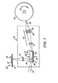
- the scanner 12 comprises an optically transparent electro-optic element 13, a linear photodetector array 14 or equivalent, and an array 15 of individually addressable electrodes 15a-15i (the arrays 14 and 15 can be seen in Figure 4).
- the photodetector array 14 and the electrode array 15 are supported on a separate substrate 16, such as a VLSI silicon circuit, and are held closely adjacent a longitudinal surface 17 of the electro-optic clement 13.
- the substrate 16 may be pressed against the electro-optic clement 13, as indicated by the arrows 18 and 19, essentially to butt the photodetector array 14 and the electrode array 15 against the surface 17.
- the document processor 11 For input scanning, the document processor 11 includes a transparent platen 21 for supporting a subject copy 22, such as an original document, which in operation is illuminated (by means not shown) and advanced (by means also not shown) in a cross line or scan pitch direction relative to the linear photodetector array 14 (i.e., longitudinally of the electro-optic element 13), as indicated by the arrow 23. Furthermore, there is an imaging lens 24 for imaging successive lines of the subject copy 22 onto the photodetector array 14 via the electro-optic element 13, thereby causing the photodetectors 14a-14i ( Figure 4) to generate data samples representing the information content of the subject copy 22. As will be seen, the optical axis 25 of the input scanner is aligned perpendicularly to the intervening pair of parallel opposed longitudinal surfaces 17 and 26 of the electro-optic clement 13 to minimize the image distorting effects of the electro-optic element 13.
- a 3 heet-like collimated light beam 31 is transmitted in a generally longitudinal direction through the electro-optic clement 13.
- the light beam 31 is supplied by a suitable source (not shown), such as a laser, and is laterally expanded to illuminate substantially the full width of the electro-optic element 13 ( Figure 3).
- Data applied to the electrodes 15a-15i create localized variations in the refractive index of the electro-optic element 13, thereby spatially modulating the phase front or polarization of the light beam 31 in accordance with such data.
- the input/output scanner 12 includes readout optics 32 for converting the phase or polarity modulation of the light beam 31 into a correspondingly modulated intensity profile, thereby providing an intensity modulated light beam 33 which is focused onto a photosensitive recording medium 34.
- the recording medium 34 is advanced in a cross line or line pitch direction relative to the light beam 33, as indicated by the arrow 35, and data samples sets representing picture elements for successive lines of an image are sequentially applied to the electrodes 15a-15i.
- the output scanner functions as a line printer.
- the electro-optic element 13 may be formed from any one of a variety of optically transparent electro-optic materials. As of now, the most promising electro-optic materials appear to be LiNbO 3 and LiTaO 3 , but there arc others which warrant consideration, including BSN, KDP, KD x P. Ba 2 NaNb 5 O 15 and PLZT.
- the input/output scanner 12 is operated in a total internal relection (TIR) mode for output scanning. Consequently, the electro-optic element 13 suitably is a y-cut crystal of, say, LiNbO 3 having opposed, optically polished input and output faces 38 and 39, respectively, and opposed, optically polished longitudinal surfaces 17 and 25, respectively. As will be seen, the longitudinal surface 17 of the crystal internally reflects the light beam 31 to achieve a TIR mode of operation.
- the light beam 31 is applied to the electro-optic clement 13 at a grazing angle of incidence relative to its longitudinal surface 17 (i.e.. an angle no greater than the critical angle of incidence for total internal reflectance therefrom) and is brought to a wedge shaped focus (by means not shown) on the reflecting surface 17 at approximately the longitudinal midline of the electrode array 15 ( Figure 4). Consequently, the light beam 31 totally internally reflects from the surface 17 and interacts, both before and after such reflection, with any electric fringe fields that have been coupled into the electro-optic clement 13 by the electrodes 15a-15i. As will be appreciated, proximity coupling is relied on in the illustrated embodiment to cause those fields to penetrate into the electro-optic element 13.
- the phase front of the light beam 31 is modulated in accordance with the data applied to the electrodes 15a-15i.
- Schlieren central dark field or bright field imaging optics are used to convert the spatial phase front modulation of the light beam 31 into a correspondingly modulated intensity profile and to supply any magnification that may be needed to obtain an image of the desired size on the recording medium 34.
- the readout optics 32 are central dark field optics comprising a field lens 41, a central stop 42, and an imaging lens 43.
- the field lens 41 is optically aligned between the output face 39 of the electro-optic element 17 and the stop 42 to focus substantially all of the zero order diffraction components of the modulated light beam 31 onto the stop 42.
- the higher order diffraction components of the light beam 31 scatter around the stop 42 and arc collected by the imaging lcns 43 to provide the intensity modulated light beam 33 for exposing the recording medium 34.
- the light beam 31 is polarized (by means not shown) before being applied to the electro-optic element 13, its polarization will be spatially modulated in accordance with the data applied to the electrodes 15a-15i.
- a polarization analyzer also not shown may be used to provide the intensity modulated light beam 33.
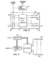
- the photodctcctor array 14 and the electrode array 15 preferably are components of a VLSI silicon circuit 16.
- Standard VLSI circuit fabrication techniques may be used to form a plurality of charge couple device (CCD) or photodiode cells 14a-14i in adjacent alignment on such a circuit, thereby defining the photodctcctor array 14.
- the metallization layer of such a circuit may be suitably patterned to define the individually addressable electrodes 15a-15i.
- the photdctcctor array 14 and the electrode array 15 are laid out in parallel spaced alignment on the VLSI circuit 16 to extend across substantially the full width of the electro-optic elcmcnt 13 ( Figure 2).
- each of the electrodes 15a-15i is about 10 ⁇ m wide, and the interelcctrodc gap spacing is about the same.
- any ratio of photodctcctor cells to individually addressable electrodes may be accommodated, even if the documcnt processor 11 is to be used for electronic copying.
- ground plane electrodes (not shown) could be interleaved with the individually addressable electrodes 15a-15i.
- the VLSI circuit 16 comprises an integrated or "on-board" parallel data processor 51 for digitizing the data samples generated-by the photodetector cells 14a-14i and for differentially encoding those samples for application to the electrodes 15a-15i, thereby enabling the document processor 11 ( Figure 1) to operate in an electronic copier mode.
- a function generator (not shown) also could be built into the data processor 51 to superimpose an electronic screening function on the differentially-encoded data for half-tone printing.
- the data processor 51 may perform, the data samples applied to the electrodes 15a-15i arc referred to hereinafter as "processed samples.” but that designation is not intended to imply that the data samples have been subjected to any particular transformation.
- serial data processor 52 which is connected to receive data samples which arc serially shifted out of the photodctector cells 14a-14i and to apply data samples to the electrodes 15a-15i via the processor 51.
- the scrial data processor 52 not only can perform the digitizing, encoding and screening functions of the parallel data processor 51, but also can accommodate communications to and from remote devices (not shown).
- a differential encoder 61 for differentially encoding the input samples on a line-by-line basis and a multiplexer 62 for rippling the encoded data samples onto the electrodes 15a-15i.
- a controller 63 synchronizes the encoder 61 and the multiplexer 62 to match the encoding rate and the ripple rate to the data rate of the serial data stream.
- data buffcrs (not shown) could be provided to allow for variations in those rates.
- each differentially encoded data sample other than the first sample for each line of the image, has a magnitude which differs from the magnitude of the previous differentially encoded sample by an amount corresponding to the magnitude of a particular input data sample.
- the first differentially encoded sample for each line of the image is referenced to a predetermined potential, such as ground.
- a predetermined potential such as ground.
- the differentially cncoded.data samples are binary digital data, but analog data may also be differentially encoded for application to the electrodes 15a-15i.
- the electrodes 15a15i could be tilted at the Bragg angle relative to the optical axis of the output scanner.
- the electrodes 15a-15i could be convergent on the entrance pupil of the imaging lens 43, thereby allowing for the use of non-telecentric imaging optics.
Landscapes
- Physics & Mathematics (AREA)
- Engineering & Computer Science (AREA)
- Multimedia (AREA)
- Signal Processing (AREA)
- Nonlinear Science (AREA)
- General Physics & Mathematics (AREA)
- Optics & Photonics (AREA)
- Facsimile Heads (AREA)
Applications Claiming Priority (2)
| Application Number | Priority Date | Filing Date | Title |
|---|---|---|---|
| US06/308,301 US4438461A (en) | 1981-10-05 | 1981-10-05 | Integrated input/output scanner for electronic document processing |
| US308301 | 1981-10-05 |
Publications (3)
| Publication Number | Publication Date |
|---|---|
| EP0076700A2 true EP0076700A2 (de) | 1983-04-13 |
| EP0076700A3 EP0076700A3 (en) | 1986-02-19 |
| EP0076700B1 EP0076700B1 (de) | 1989-03-08 |
Family
ID=23193412
Family Applications (1)
| Application Number | Title | Priority Date | Filing Date |
|---|---|---|---|
| EP82305305A Expired EP0076700B1 (de) | 1981-10-05 | 1982-10-05 | Eingabe-Ausgabe-Abtastanlage für die Verarbeitung von Dokumenten |
Country Status (3)
| Country | Link |
|---|---|
| US (1) | US4438461A (de) |
| EP (1) | EP0076700B1 (de) |
| DE (1) | DE3279528D1 (de) |
Cited By (3)
| Publication number | Priority date | Publication date | Assignee | Title |
|---|---|---|---|---|
| GB2186462A (en) * | 1985-12-23 | 1987-08-12 | Sharp Kk | Read/record head in facsimile |
| EP0634800A1 (de) * | 1993-07-12 | 1995-01-18 | Philips Electronics Uk Limited | Bildaufnahmevorrichtung |
| US7591971B2 (en) | 2002-01-22 | 2009-09-22 | Weidmann Plastics Technology Ag | Method for producing an adhesive molded body |
Families Citing this family (3)
| Publication number | Priority date | Publication date | Assignee | Title |
|---|---|---|---|---|
| US4679215A (en) * | 1985-12-06 | 1987-07-07 | Sperry Corporation | Exceedance counting integrating photo-diode array |
| FR2726422B1 (fr) * | 1994-10-31 | 1997-01-17 | Sgs Thomson Microelectronics | Detecteur de reception d'un signal de television couleur code selon la norme secam |
| KR100319206B1 (ko) * | 1998-10-20 | 2002-01-10 | 윤종용 | 박막트랜지스터 제조방법과 이에 의해 제조된 기판 및 박막트랜지스터 |
Family Cites Families (8)
| Publication number | Priority date | Publication date | Assignee | Title |
|---|---|---|---|---|
| US4060319A (en) * | 1975-06-20 | 1977-11-29 | Meaney Jr Daniel J | Coherent beam imaging apparatus and method |
| FR2404272A1 (fr) * | 1977-09-23 | 1979-04-20 | Thomson Csf | Dispositif de reproduction d'images monochromes et systeme de teletransmission d'images utilisant un tel dispositif |
| US4241990A (en) | 1979-03-05 | 1980-12-30 | Xerox Corporation | Multi-purpose optical data processor |
| US4281904A (en) | 1979-06-21 | 1981-08-04 | Xerox Corporation | TIR Electro-optic modulator with individually addressed electrodes |
| US4356347A (en) | 1980-08-25 | 1982-10-26 | Xerox Corporation | Integrated stylus array for printer operation |
| AU543324B2 (en) * | 1980-09-17 | 1985-04-18 | Xerox Corporation | Electro-optical line printer |
| US4367925A (en) | 1980-09-17 | 1983-01-11 | Xerox Corporation | Integrated electronics for proximity coupled electro-optic devices |
| US4374617A (en) | 1981-08-05 | 1983-02-22 | Xerox Corporation | Multi-function document processor |
-
1981
- 1981-10-05 US US06/308,301 patent/US4438461A/en not_active Expired - Fee Related
-
1982
- 1982-10-05 DE DE8282305305T patent/DE3279528D1/de not_active Expired
- 1982-10-05 EP EP82305305A patent/EP0076700B1/de not_active Expired
Cited By (5)
| Publication number | Priority date | Publication date | Assignee | Title |
|---|---|---|---|---|
| GB2186462A (en) * | 1985-12-23 | 1987-08-12 | Sharp Kk | Read/record head in facsimile |
| US4809080A (en) * | 1985-12-23 | 1989-02-28 | Sharp Kabushiki Kaisha | Read/record head in facsimile |
| GB2186462B (en) * | 1985-12-23 | 1989-12-06 | Sharp Kk | Facsimile apparatus read and record heads |
| EP0634800A1 (de) * | 1993-07-12 | 1995-01-18 | Philips Electronics Uk Limited | Bildaufnahmevorrichtung |
| US7591971B2 (en) | 2002-01-22 | 2009-09-22 | Weidmann Plastics Technology Ag | Method for producing an adhesive molded body |
Also Published As
| Publication number | Publication date |
|---|---|
| DE3279528D1 (en) | 1989-04-13 |
| EP0076700B1 (de) | 1989-03-08 |
| US4438461A (en) | 1984-03-20 |
| EP0076700A3 (en) | 1986-02-19 |
Similar Documents
| Publication | Publication Date | Title |
|---|---|---|
| US4636039A (en) | Nonuniformity of fringe field correction for electro-optic devices | |
| EP0550189B1 (de) | Bildgenerator mit elektrooptischen TIR-Lichtmodulator, der eine Vielzahl von Elektroden pro Bildpunkt aufweist | |
| EP0087970B1 (de) | Lineare Modulatoren | |
| US4367925A (en) | Integrated electronics for proximity coupled electro-optic devices | |
| CA1171508A (en) | Proximity coupled electro-optic devices | |
| US4450459A (en) | Differential encoding for fringe field responsive electro-optic line printers | |
| US4480899A (en) | Two dimensional electro-optic modulator and applications therefor | |
| US4673953A (en) | Interpixel null suppression for optical image bars | |
| EP0061926B1 (de) | Mehrweg-Lichtventil für elektrooptische Zeilendrucker mit nicht telezentrischen Abbildungssystemen | |
| US4560994A (en) | Two dimensional electro-optic modulator for printing | |
| US4421387A (en) | Extended thin film light modulator/scanner | |
| EP0076700B1 (de) | Eingabe-Ausgabe-Abtastanlage für die Verarbeitung von Dokumenten | |
| US4376568A (en) | Thick film line modulator | |
| CA1178326A (en) | Electro-optic line printer | |
| US4940314A (en) | Variable wavelength discrete optical image bars having passively enhanced spatial addressing capacity | |
| US4437106A (en) | Method and means for reducing illumination nulls in electro-optic line printers | |
| US4415915A (en) | Multilayer interleaved electrodes for multigate light valves | |
| JPH0356638B2 (de) | ||
| EP0229506B1 (de) | Optischer Bildgenerator | |
| US5191464A (en) | Electrooptic TIR light modulator image bar having spatial filter for optimizing spatial frequency response | |
| US5218469A (en) | Electrooptic TIR light modulator image bar having illumination conditions for optimizing spatial frequency response | |
| EP0048595B1 (de) | Vorrichtung zum zeilenweisen Drucken | |
| US5255118A (en) | Electrooptic TIR light modulator image bar having electrode length for optimizing spatial frequency response | |
| EP0072124A1 (de) | Lichtmodulationsvorrichtung mit einem Mehrtor-Lichtventil | |
| US20050116141A1 (en) | Method, assemblage, and scanner for optically sampling light by a photosensitive device |
Legal Events
| Date | Code | Title | Description |
|---|---|---|---|
| PUAI | Public reference made under article 153(3) epc to a published international application that has entered the european phase |
Free format text: ORIGINAL CODE: 0009012 |
|
| AK | Designated contracting states |
Designated state(s): DE FR GB |
|
| PUAL | Search report despatched |
Free format text: ORIGINAL CODE: 0009013 |
|
| AK | Designated contracting states |
Designated state(s): DE FR GB |
|
| 17P | Request for examination filed |
Effective date: 19860809 |
|
| 17Q | First examination report despatched |
Effective date: 19871105 |
|
| GRAA | (expected) grant |
Free format text: ORIGINAL CODE: 0009210 |
|
| AK | Designated contracting states |
Kind code of ref document: B1 Designated state(s): DE FR GB |
|
| REF | Corresponds to: |
Ref document number: 3279528 Country of ref document: DE Date of ref document: 19890413 |
|
| EN | Fr: translation not filed | ||
| PLBE | No opposition filed within time limit |
Free format text: ORIGINAL CODE: 0009261 |
|
| STAA | Information on the status of an ep patent application or granted ep patent |
Free format text: STATUS: NO OPPOSITION FILED WITHIN TIME LIMIT |
|
| 26N | No opposition filed | ||
| PGFP | Annual fee paid to national office [announced via postgrant information from national office to epo] |
Ref country code: FR Payment date: 19910823 Year of fee payment: 10 |
|
| PGFP | Annual fee paid to national office [announced via postgrant information from national office to epo] |
Ref country code: GB Payment date: 19940907 Year of fee payment: 13 |
|
| PGFP | Annual fee paid to national office [announced via postgrant information from national office to epo] |
Ref country code: DE Payment date: 19940915 Year of fee payment: 13 |
|
| PG25 | Lapsed in a contracting state [announced via postgrant information from national office to epo] |
Ref country code: GB Effective date: 19951005 |
|
| GBPC | Gb: european patent ceased through non-payment of renewal fee |
Effective date: 19951005 |
|
| PG25 | Lapsed in a contracting state [announced via postgrant information from national office to epo] |
Ref country code: DE Effective date: 19960801 |
|
| PG25 | Lapsed in a contracting state [announced via postgrant information from national office to epo] |
Ref country code: FR Free format text: LAPSE BECAUSE OF FAILURE TO SUBMIT A TRANSLATION OF THE DESCRIPTION OR TO PAY THE FEE WITHIN THE PRESCRIBED TIME-LIMIT Effective date: 20001031 |
|
| PG25 | Lapsed in a contracting state [announced via postgrant information from national office to epo] |
Ref country code: FR Free format text: LAPSE BECAUSE OF FAILURE TO SUBMIT A TRANSLATION OF THE DESCRIPTION OR TO PAY THE FEE WITHIN THE PRESCRIBED TIME-LIMIT Effective date: 19921031 |