EP0076736B1 - Integrierte Schaltung mit induktivem Verhalten und Filter mit einer solchen Schaltung - Google Patents
Integrierte Schaltung mit induktivem Verhalten und Filter mit einer solchen Schaltung Download PDFInfo
- Publication number
- EP0076736B1 EP0076736B1 EP82401753A EP82401753A EP0076736B1 EP 0076736 B1 EP0076736 B1 EP 0076736B1 EP 82401753 A EP82401753 A EP 82401753A EP 82401753 A EP82401753 A EP 82401753A EP 0076736 B1 EP0076736 B1 EP 0076736B1
- Authority
- EP
- European Patent Office
- Prior art keywords
- capacitor
- terminal
- circuit
- operational amplifier
- cycle
- Prior art date
- Legal status (The legal status is an assumption and is not a legal conclusion. Google has not performed a legal analysis and makes no representation as to the accuracy of the status listed.)
- Expired
Links
- 230000001939 inductive effect Effects 0.000 title 1
- 239000003990 capacitor Substances 0.000 claims description 39
- 230000000737 periodic effect Effects 0.000 claims description 3
- 238000010586 diagram Methods 0.000 description 4
- 238000005516 engineering process Methods 0.000 description 3
- 230000000903 blocking effect Effects 0.000 description 2
- 235000021183 entrée Nutrition 0.000 description 2
- 239000004065 semiconductor Substances 0.000 description 2
- 238000006842 Henry reaction Methods 0.000 description 1
- 238000004364 calculation method Methods 0.000 description 1
- 235000019994 cava Nutrition 0.000 description 1
- 238000007599 discharging Methods 0.000 description 1
- 230000000694 effects Effects 0.000 description 1
- 238000004519 manufacturing process Methods 0.000 description 1
- 238000000034 method Methods 0.000 description 1
- 230000003071 parasitic effect Effects 0.000 description 1
- 238000000819 phase cycle Methods 0.000 description 1
- 230000003252 repetitive effect Effects 0.000 description 1
- 239000007787 solid Substances 0.000 description 1
- 229910000648 terne Inorganic materials 0.000 description 1
- 230000017105 transposition Effects 0.000 description 1
Images

Classifications
-
- H—ELECTRICITY
- H03—ELECTRONIC CIRCUITRY
- H03H—IMPEDANCE NETWORKS, e.g. RESONANT CIRCUITS; RESONATORS
- H03H19/00—Networks using time-varying elements, e.g. N-path filters
- H03H19/004—Switched capacitor networks
- H03H19/006—Switched capacitor networks simulating one-port networks
Definitions
- the present invention relates to integrated circuits, and more particularly to the field of filters.
- inductors cannot be produced using integrated circuit manufacturing techniques, especially if they must be of high value.
- a fully integratable circuit element is produced in a particularly simple manner which has an inductance characteristic which can have a very high value (several henrys), this element being able to be associated with other circuit elements to produce filters built on ladder passive filter diagrams with inductances and capacities.
- patent EP-A-0024011 An example of an integrated simulated inductance diagram is presented in patent EP-A-0024011. It essentially comprises an operational amplifier, three capacities and five switches working in a cycle of four distinct phases.
- the present invention proposes an even simpler circuit since it essentially comprises, in addition to the operational amplifier, only two capacities and three switches working according to a three-phase cycle.
- the whole is preferably integrable according to a MOS (metal-oxide-semiconductor) technology: there have long been good operational amplifiers made in this technology, the switches can be made each by an MOS transistor, and the capacities, of the order of a few tens or hundreds of picofarads, can be produced by using as dielectric, between two conductive layers, the thin oxide used to form the MOS transistors.
- MOS metal-oxide-semiconductor
- the second terminal of the circuit can be confused with a ground terminal if, for example, the inductance is mounted between a signal terminal and ground.
- inductor is inserted in series in a circuit, two specific switches must be provided to connect the first capacitor either to earth (steps b, c) or to the second terminal of the circuit (steps a and d).
- the value of the inductance is equal to CI / Co 2 f z if Co and CI are the values of the first and second capacitances and f the frequency of the repetitive cycle for controlling the switches.
- the inductance being in principle used in combination with a capacity to produce plug circuits whose resonant frequency depends on the product of the inductance by the capacity, it is seen that this frequency will be essentially a function of a capacity ratio.
- this frequency will be essentially a function of a capacity ratio.
- the switching frequency f can also be very well known, so that the LC filters produced with this simulated inductance will have resonance frequencies which can be very precisely defined.
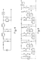
- the circuit of the invention represented in FIG. 1, has two terminals A and B, the terminal B here being connected to ground to produce a circuit simulating an inductance connected between a signal terminal (terminal A) and ground .
- the circuit comprises a first capacitor Co in series with a switch constituted here by an insulated gate transistor (MOS), T1, this assembly in series being connected between the terminals A and B.
- MOS insulated gate transistor
- a second switch also constituted and represented by a MOS transistor, T2 is connected between the junction point of the capacitor Co and of the transistor T1 and the inverting input of an operational amplifier AO (whose non-inverting input is at the mass).
- a third switch constituted and represented by a MOS transistor, T3, is connected between the output of the operational amplifier and the junction point between the first capacitor Co and the transistors T1 and T2.
- a second capacitor C1 is connected between the output and the inverting input of the operational amplifier A0 to serve as a capacitive feedback to this amplifier.
- a switching control logic circuit controls the gates of the three transistors to make them conductive or block them according to a periodic cycle at a switching frequency f significantly higher than the probable frequencies of the signals applied to terminal A.
- the control cycle is such that the transistors are made conductive during disjoint time intervals, that is to say that only one transistor at a time is conductive during each phase of the cycle.
- the conduction times of each transistor therefore correspond to a fraction of the period of the switching cycle.
- FIGS. 2a, 2b and 2c respectively represent the first, the second and the third phase of the switching cycle at the frequency f.
- the first phase of the following cycle that is to say of the cycle i + 1, consists in making the transistor T1 conductive (the others being blocked).
- the capacitor Co is then charged at the voltage E; this charge takes place very quickly because the capacitance has a low value, and it is terminated before the transistor turns off.
- the capacity is of the order of 100 picofarads,.
- a closing time of a fraction of a microsecond must be provided, which gives an overview of the maximum order of magnitude of the frequency f of. switching cycle.
- the output voltage V, of the amplifier AO did not vary because it is assumed that it is a perfect operational amplifier with infinite input impedance and high gain, and the capacity of C1, charged at voltage V, could not discharge.
- the charge for capacity C1 was initially C1V ; . It therefore becomes C1V i - CoE. As the voltage at the inverting input of the amplifier is brought back to zero (potential of the non-inverting input), it is the output voltage of the amplifier which varies and which becomes V ; + such that: or
- the third phase (FIG. 2c) then consists in applying this new voltage to the capacitor Co.
- the switch constituted by the transistor T2 is opened and the one constituted by the transistor T3 is closed.
- the capacitance Co is thus connected between the output (at V i + 1 ) of the amplifier and the ground. It will be noted that the capacitor Co charges at V i + 1 without the capacitor C1 discharging (and therefore without modifying the output voltage V i + 1 ) because the capacitor C1 is in series with the input impedance assumed to be infinite of the AO amplifier.
- FIG. 3 represents an alternative embodiment of a circuit intended to replace an inductor in series between two points, none of which constitutes a mass of the circuit or a fixed voltage reference point.
- FIG. 3 The circuit of FIG. 3 is the same as that of FIG. 2 with the exception of the connection between the first capacitor Co and the terminal B: this connection was direct in FIG. 2; in Figure 3, this connection is made through a fourth switch (transistor T4) to terminal B and through a fifth switch (transistor T5) to ground.
- the transistors T4 and T5 are controlled, like the transistors T1, T2 and T3, by the logic circuit CL not shown in FIG. 3.
- the operation differs from that of FIG. 2 in the sense that the first phase additionally comprises the blocking of the transistor T5 and the switching on of the transistor T4, while the second and the third phase comprise the switching on of the transistor T5 and blocking of transistor T4 after transistor T1 has been blocked.
- the conduction phases of transistors T4 and T5 are separated so that there is no risk of grounding of terminal B.
- those of conduction of T1 and T5 are dissociated, like those of T1, T2, those of T1, T3 and those of T2, T3.
- FIG. 4 shows by way of example a conventional passive filter of the 12th order (bandpass filter) using a network of inductances and capacitors in scale
- FIG. 5 shows a filter which is the transposition thereof according to the invention , in which the resistors have been replaced by switched capacitors and the inductors by circuits conforming to FIG. 1 or 3.
- the number of operational amplifiers of this twelfth order filter is only six ( in addition to the output impedance adapter).
- the logic circuit CL for switching control of the various switches is not shown in FIG. 5.
Landscapes
- Engineering & Computer Science (AREA)
- Power Engineering (AREA)
- Networks Using Active Elements (AREA)
- Filters That Use Time-Delay Elements (AREA)
Claims (4)
Applications Claiming Priority (2)
| Application Number | Priority Date | Filing Date | Title |
|---|---|---|---|
| FR8118636 | 1981-10-02 | ||
| FR8118636A FR2514216B1 (fr) | 1981-10-02 | 1981-10-02 | Circuit integre a caracteristique inductive et filtre utilisant ce circuit |
Publications (2)
| Publication Number | Publication Date |
|---|---|
| EP0076736A1 EP0076736A1 (de) | 1983-04-13 |
| EP0076736B1 true EP0076736B1 (de) | 1986-04-16 |
Family
ID=9262706
Family Applications (1)
| Application Number | Title | Priority Date | Filing Date |
|---|---|---|---|
| EP82401753A Expired EP0076736B1 (de) | 1981-10-02 | 1982-09-28 | Integrierte Schaltung mit induktivem Verhalten und Filter mit einer solchen Schaltung |
Country Status (5)
| Country | Link |
|---|---|
| US (1) | US4513265A (de) |
| EP (1) | EP0076736B1 (de) |
| JP (1) | JPS5871711A (de) |
| DE (1) | DE3270650D1 (de) |
| FR (1) | FR2514216B1 (de) |
Families Citing this family (3)
| Publication number | Priority date | Publication date | Assignee | Title |
|---|---|---|---|---|
| IT1220191B (it) * | 1987-12-22 | 1990-06-06 | Sgs Thomson Microelectronics | Filtro attivo passabasso del primo ordine integrato |
| USRE35494E (en) * | 1987-12-22 | 1997-04-22 | Sgs-Thomson Microelectronics, S.R.L. | Integrated active low-pass filter of the first order |
| EP1248367A1 (de) * | 2001-04-03 | 2002-10-09 | Alcatel | Aktive Schaltung zur Simulierung einer Induktivität |
Family Cites Families (2)
| Publication number | Priority date | Publication date | Assignee | Title |
|---|---|---|---|---|
| EP0024011B1 (de) * | 1979-08-09 | 1983-08-31 | Siemens Aktiengesellschaft | Elektrische Filterschaltung unter Verwendung von wenigstens einer simulierten Induktivität, die gesteuerte Schalter, Kondensatoren und Verstärker enthält |
| DE3001969C2 (de) * | 1980-01-21 | 1982-10-28 | Siemens AG, 1000 Berlin und 8000 München | Elektrische Filterschaltung unter Verwendung von wenigstens einer simulierten Induktivität, die gesteuerte Schalter, Kondensatoren und Verstärker enthält |
-
1981
- 1981-10-02 FR FR8118636A patent/FR2514216B1/fr not_active Expired
-
1982
- 1982-09-24 US US06/422,390 patent/US4513265A/en not_active Expired - Lifetime
- 1982-09-28 EP EP82401753A patent/EP0076736B1/de not_active Expired
- 1982-09-28 DE DE8282401753T patent/DE3270650D1/de not_active Expired
- 1982-10-02 JP JP57172548A patent/JPS5871711A/ja active Pending
Also Published As
| Publication number | Publication date |
|---|---|
| JPS5871711A (ja) | 1983-04-28 |
| US4513265A (en) | 1985-04-23 |
| DE3270650D1 (en) | 1986-05-22 |
| EP0076736A1 (de) | 1983-04-13 |
| FR2514216B1 (fr) | 1986-07-18 |
| FR2514216A1 (fr) | 1983-04-08 |
Similar Documents
| Publication | Publication Date | Title |
|---|---|---|
| EP0030173B1 (de) | Ladungsverschiebungsfilter mit geschalteten Kapazitäten | |
| CN101356731B (zh) | 电荷采样滤波器电路和电荷采样方法 | |
| EP1646147A1 (de) | Analoges Filter für zeitdiskrete Signale aus passiven Bauelementen | |
| EP0307276A1 (de) | Bemusterte Filtereinrichtung mit geschalteten Kapazitäten | |
| FR2597279A1 (fr) | Procede et circuit pour l'utilisation de condensateurs en temps partage | |
| WO2002054167A1 (fr) | Regulateur de tension a stablite amelioree | |
| EP0660512B1 (de) | Phasenschiebverstärker und seine Verwendung in einer Zusammenführungsschaltung | |
| EP0409747A1 (de) | Gate-Steuerschaltung für einen MOS-Transistor | |
| CH625373A5 (de) | ||
| EP0307275B1 (de) | Filter-Vierpol mit geschalteten Kapazitäten zur Linearisierung der Phasen/Frequenz-Wiedergabe dieses Filters | |
| EP0847626B1 (de) | Vorrichtung zur digitalverarbeitung eines analogsignals, welches auch wieder in analoger form ausgegeben werden soll | |
| FR2767977A1 (fr) | Etage de sortie pour pompe de charge faible courant et demodulateur integrant une telle pompe de charge | |
| FR2589266A1 (fr) | Integrateur differentiel a un seul condensateur | |
| EP0695035A1 (de) | Mehrfachvergleichs-A/D-Wandler unter Anwendung des Interpolationsprinzips | |
| EP0076736A1 (de) | Integrierte Schaltung mit induktivem Verhalten und Filter mit einer solchen Schaltung | |
| FR2472306A1 (fr) | Filtre elliptique a condensateurs commutes | |
| EP0143024B1 (de) | Mit geschalteten Kapazitäten durchgeführter exponentieller Integrator mit erhöhter Zeitkonstante | |
| EP0012667B1 (de) | Verfahren zum Filtern eines elektrischen Signals durch Ladungsübertragung in einem Halbleiter und Filter mit geschalteten Kondensatoren, das dieses Verfahren verwendet | |
| EP0757427B1 (de) | Phasengeneratorschaltung für eine negative Spannungsversorgungsschaltung des Ladungspumpen-Typs | |
| EP0076737A1 (de) | Symmetrischer Integrator und dessen Anwendung in einem Filter | |
| FR2838890A1 (fr) | Circuit de filtre a condensateur commute et procede pour sa fabrication | |
| EP0346988A2 (de) | Integrierte Halbleiterschaltung mit synchronisiertem Komparator | |
| FR2513832A1 (fr) | Dispositif de lecture en courant d'une quantite de charges electriques et filtre a transfert de charges muni d'un tel dispositif | |
| FR2575013A1 (fr) | Porte logique a coincidence, et circuits logiques sequentiels mettant en oeuvre cette porte a coincidence | |
| FR2604834A1 (fr) | Redresseur double alternance a capacites commutees |
Legal Events
| Date | Code | Title | Description |
|---|---|---|---|
| PUAI | Public reference made under article 153(3) epc to a published international application that has entered the european phase |
Free format text: ORIGINAL CODE: 0009012 |
|
| AK | Designated contracting states |
Designated state(s): DE FR GB IT NL |
|
| 17P | Request for examination filed |
Effective date: 19830420 |
|
| GRAA | (expected) grant |
Free format text: ORIGINAL CODE: 0009210 |
|
| AK | Designated contracting states |
Kind code of ref document: B1 Designated state(s): DE FR GB IT NL |
|
| ITF | It: translation for a ep patent filed | ||
| REF | Corresponds to: |
Ref document number: 3270650 Country of ref document: DE Date of ref document: 19860522 |
|
| PLBE | No opposition filed within time limit |
Free format text: ORIGINAL CODE: 0009261 |
|
| STAA | Information on the status of an ep patent application or granted ep patent |
Free format text: STATUS: NO OPPOSITION FILED WITHIN TIME LIMIT |
|
| 26N | No opposition filed | ||
| PGFP | Annual fee paid to national office [announced via postgrant information from national office to epo] |
Ref country code: NL Payment date: 19900930 Year of fee payment: 9 |
|
| ITTA | It: last paid annual fee | ||
| PG25 | Lapsed in a contracting state [announced via postgrant information from national office to epo] |
Ref country code: NL Effective date: 19920401 |
|
| NLV4 | Nl: lapsed or anulled due to non-payment of the annual fee | ||
| REG | Reference to a national code |
Ref country code: FR Ref legal event code: D6 |
|
| PGFP | Annual fee paid to national office [announced via postgrant information from national office to epo] |
Ref country code: FR Payment date: 20010911 Year of fee payment: 20 |
|
| PGFP | Annual fee paid to national office [announced via postgrant information from national office to epo] |
Ref country code: GB Payment date: 20010926 Year of fee payment: 20 |
|
| PGFP | Annual fee paid to national office [announced via postgrant information from national office to epo] |
Ref country code: DE Payment date: 20011015 Year of fee payment: 20 |
|
| REG | Reference to a national code |
Ref country code: GB Ref legal event code: IF02 |
|
| PG25 | Lapsed in a contracting state [announced via postgrant information from national office to epo] |
Ref country code: GB Free format text: LAPSE BECAUSE OF EXPIRATION OF PROTECTION Effective date: 20020927 |
|
| REG | Reference to a national code |
Ref country code: GB Ref legal event code: PE20 Effective date: 20020927 |