EP0077266B1 - Switched capacitor automatic gain control loop - Google Patents
Switched capacitor automatic gain control loop Download PDFInfo
- Publication number
- EP0077266B1 EP0077266B1 EP82401843A EP82401843A EP0077266B1 EP 0077266 B1 EP0077266 B1 EP 0077266B1 EP 82401843 A EP82401843 A EP 82401843A EP 82401843 A EP82401843 A EP 82401843A EP 0077266 B1 EP0077266 B1 EP 0077266B1
- Authority
- EP
- European Patent Office
- Prior art keywords
- output
- control circuit
- gain control
- automatic gain
- lead
- Prior art date
- Legal status (The legal status is an assumption and is not a legal conclusion. Google has not performed a legal analysis and makes no representation as to the accuracy of the status listed.)
- Expired
Links
- 239000003990 capacitor Substances 0.000 title claims description 135
- 230000007423 decrease Effects 0.000 claims description 11
- 230000003247 decreasing effect Effects 0.000 claims description 9
- 238000000034 method Methods 0.000 claims description 4
- 238000003491 array Methods 0.000 description 11
- 230000010354 integration Effects 0.000 description 9
- 230000005540 biological transmission Effects 0.000 description 5
- 238000010586 diagram Methods 0.000 description 5
- 230000000694 effects Effects 0.000 description 4
- 230000035945 sensitivity Effects 0.000 description 3
- 238000005516 engineering process Methods 0.000 description 2
- 230000001052 transient effect Effects 0.000 description 2
- XUIMIQQOPSSXEZ-UHFFFAOYSA-N Silicon Chemical compound [Si] XUIMIQQOPSSXEZ-UHFFFAOYSA-N 0.000 description 1
- 230000015572 biosynthetic process Effects 0.000 description 1
- 235000019994 cava Nutrition 0.000 description 1
- 230000007547 defect Effects 0.000 description 1
- 238000007599 discharging Methods 0.000 description 1
- 230000005669 field effect Effects 0.000 description 1
- 238000001914 filtration Methods 0.000 description 1
- 230000001771 impaired effect Effects 0.000 description 1
- 229910044991 metal oxide Inorganic materials 0.000 description 1
- 150000004706 metal oxides Chemical class 0.000 description 1
- 239000004065 semiconductor Substances 0.000 description 1
- 229910052710 silicon Inorganic materials 0.000 description 1
- 239000010703 silicon Substances 0.000 description 1
- 230000005236 sound signal Effects 0.000 description 1
Images


Classifications
-
- H—ELECTRICITY
- H03—ELECTRONIC CIRCUITRY
- H03G—CONTROL OF AMPLIFICATION
- H03G1/00—Details of arrangements for controlling amplification
- H03G1/0005—Circuits characterised by the type of controlling devices operated by a controlling current or voltage signal
- H03G1/0088—Circuits characterised by the type of controlling devices operated by a controlling current or voltage signal using discontinuously variable devices, e.g. switch-operated
- H03G1/0094—Circuits characterised by the type of controlling devices operated by a controlling current or voltage signal using discontinuously variable devices, e.g. switch-operated using switched capacitors
Definitions
- This invention relates to automatic gain control circuits, and more specifically to an automatic gain control circuit utilizing switched capacitors which is capable of being implemented as a monolithic integrated circuit device.
- AGC Automatic gain control circuits
- Such automatic gain control circuits operate to provide an output signal having a relatively fixed amplitude despite wide variations in input signal amplitudes.
- Such AGC circuits have been used for many years in, for example, radio receivers and audio equipment, as well as in many other applications and have been disclosed for example in UK Patent GB-A-1 342 383.
- the gain control is obtained by varying the gain in steps of a linear signal transfer device through a forward reverse counter driven by a twin comparator which is fed from the output signal through an envelope detector.
- the present invention seeks to overcome the foregoing defects or disadvantages and to provide an AGC circuit in which the gain control is such that the gain variations are always related to each other in a simple relation and the sensitivity of which is not impaired by the choice of a preset voltage gap so as to enable good use of the signal handling capacity of the circuit of the invention to be achieved.
- an AGC circuit utilizing MOS devices and switched capacity technology is fabricated on a single semiconductor chip.
- the AGC circuct constructed in accordance with this invention contains a programmable gain storage comprising an operational amplifier and one or more capacitors arrays for controlling the closed loop gain of the operation amplifier.
- the gain of the operational amplifier is automatically controlled to produce an output signal of desired amplitude.
- the output signal of this operational amplifier is rectified, and the rectified signal (hereinafter referred to as the "rectified AGC signal”) is integrated utilizing an integrator stage of well-known design.
- a reference voltage of opposite polarity to the rectified AGC signal is also integrated on the integrator stage and the output signal of the integrator is compared to ground, thereby obtaining the sign bit of the output signal of the integrator stage.
- the sign bit indicating the polarity is stored in a latch, and is used to operate a counter stage, with the counter stage increasing its count by one count during each clock period in which the sign bit is a logical zero, corresponding to a period when the amplitude of the output signal of the AGC circuit is higher than desired.
- the counter stage decreases its count by one count during each clock period when the sign bit is a logical one, corresponding to a period when the amplitude of the output signal of the AGC circuit is lower than desired.
- the output bits of the counter are used to control switches in the one or more capacitor arrays which control the closed loop gain of the operational amplifier of the AGC circuit of this invention.
- the sign bit when the magnitude of the output signal from the AGC circuit of this invention is less than desired, the sign bit will be equal to one, thereby causing the counter to count down, thereby controlling the capacitors in the one or more capacitor arrays so as to increase the closed loop gain of the operational amplifier.
- the sign bit if the amplitude of the AGC output signal is greater than desired, the sign bit will be equal to zero, thereby causing the counter to count up, thereby controlling the capacitors in the one or more capacitor arrays so as to decrease the closed loop gain of the operational amplifier.
- the sign bit When the AGC circuit of this invention has stabilized, the sign bit will toggle between one and zero during alternate clock periods, thus causing the counter to alternately count up and down, thereby in effect continuously toggling the binary output signal from the counter by one. This causes the capacitors in the one or more capacitor arrays to be controlled in such a manner as to cause the closed loop gain of the operational amplifier to toggle between two closely related values, thereby providing an output signal of relatively constant amplitude, as desired.
- Another embodiment of this invention utilizes a plurality of capacitors which are selectively connected to the integration stage, thereby providing a plurality of possible response times of the AGC circuit.
- the automatic gain control circuit of this invention will be easily understood in conjunction with Figure 1.
- the automatic gain control circuit 10 includes operational amplifier 150 constructed in a well-known manner.
- the non-inverting input lead 137 of operational amplifier 150 is connected to ground, although it is to be understood that non-inverting input lead 137 may be connected to any suitable reference voltage.
- Capacitor 102 is connected between input terminal 100, to which the input voltage to be controlled (V 1N ) is applied, and inverting input lead 136 of operational amplifier 150.
- Capacitor array 121 is connected between inverting input lead 136 and output terminal 155 of operational amplifier 150, thereby providing negative feedback.
- Capacitor 102 and capacitor array 121 operate in a well-known manner to control the closed loop gain of operational- amplifier 150.
- the closed loop gain G 1 of operational amplifier 150 is equal to where
- Capacitor array 121 comprises a plurality of N capacitors 125-1 through 125-N connected between inverting input lead 136 and output terminal 155 of operational amplifier 150.
- Capacitors 125-2 through 125-N of capacitor array 121 are selectively connected in parallel with capacitor 125-1 by the operation of appropriate switches 134-2 through 134-N and 135-2 through 135-N. For example, capacitor 125-2 is connected in parallel with capacitor 125-1 when switches 134-2 and 135-2 are closed, and is disconnected when switches 134-2 and 135-2 are open.
- capacitors 125-1 through 125-N in capacitor array 121 may be equally weighted, such that the capacitance of capacitor array 121 connected between output terminal 155 and lead 136 may be selected in accordance with the following equation:
- the effective capacitance of binary weighted array 121 is equal to where K is an integer ranging from 1 to (2 N -1), and where N is the number of capacitors in capacitor array 121.
- the capacitance values of capacitors 125-1 through 125-N of capacitor array 121 may also be selected in accordance with any other desired weighting scheme including, but not limited to, weighting schemes which allow companding in accordance with the well known p255 law specified by documents available from the International Brass and Telephone Consultative Committee (CCITT) (Europe) and by the American Telephone and Telephone Company (AT&T) (USA).
- the switches within capacitor array 121 are controlled by the counter 200 in order to select the desired closed loop of operational amplifier 150, as will be more fully described later.
- the output signal available on output terminal 155 of operational amplifier 150 is rectified by diode bridge 156 and alternately integrated with a reference voltage V ref in integrator stage 300.
- Rectifier bridge 156 may be replaced with any suitable rectifying means, including a half-wave rectifier comprising a single diode.
- the magnitude of reference voltage V ref must be decreased by approximately 50% if half-wave rectification of output signal V o is used in place of full-wave rectification.
- Integrator 300 comprises operational amplifier 170, integrating capacitor 174, and switches 173, 175 and 176.
- Diodes can be fabricated MOS devices, but one terminal of the diode is connected to a supply voltage. Alternatively, transistors may be used in place of the diodes, but transistors have current gain.
- the circuit of Figure 5 may be used in place of bridge rectifier 156 (Fig. 1) to rectify the output signal from operational amplifier 150 for application to capacitor 160.
- Input terminal 700 of rectifier means 699 is connected to node 700 of Figure 1, and outputterminal 701 of rectifier 699 is connected to node 701 of the circuit of Figure 1.
- Node 702 of the circuit of Figure 1 is connected to ground when rectifier 699 is utilized.
- Rectifier 699 comprises operational amplifier 702, having its inverted input terminal connected to ground, and its non-inverting input terminal connected to input terminal 700.
- operational amplifier 702 functions as a voltage comparator and provides a positive output signal when the input signal applied to terminal 700 is positive.
- operational amplifier 702 provides a negative output signal when the signal applied to terminal 700 is negative.
- Operational amplifier 705 has its non-inverting input lead connected to ground, and its inverting input lead connected to input terminal 700 through resistor 703. Negative feedback is provided between the output lead of operational amplifier 705 and the inverting input lead of operational amplifier 705 by resistor 704.
- operational amplifier 705 provides on its output lead a voltage of polarity opposite to the voltage V o applied to terminal 700.
- Operational amplifier 706 having its inverting input lead connected to its output lead, and its non-inverting input lead connected to terminal 700, serves as a unity-gain amplifier, thus providing a voltage on its output lead which is of the same polarity as the voltage applied to terminal 700.
- Transmission gates 708 (comprising N-Channel MOSFET 708a and P-Channel MOSFET 708b) and 709 (comprising N-Channel MOSFET 709a and P-Channel MOSFET 709b serve to couple the desired voltage from the output leads of operational amplifiers 705 and 706 to output terminal 701 of rectifier 699.
- operational amplifier 702 provides a positive voltage on its output lead which is applied to the gates of P-Channel MOSFET 708b and N-Channel MOSFET 709a, thus turning off MOSFET 708b and turning on MOSFET 709a.
- the positive voltage provided on the output lead of operational amplifier 702 is inverted by inverter 707, thus providing a negative voltage on the gates of N-Channel MOSFET 708a and P-Channel MOSFET 709b, thus turning off transistor 708a and turning on transistor 709b.
- transmission gate 708 is turned off and transmission gate 709 is turned on, thus connecting the positive voltage from unit gain amplifier 706 to terminal 701.
- operational amplifier 702 provides a negative voltage on its output lead, thus causing transmission gate 708 to turn on and transmission gate 709 to turn off.
- the rectifier means 699 of Figure 5 operates to rectify the input voltage applied to its terminal 700 and provides the rectified voltage on its output terminal 701.
- Integrator stage 300 is initialized during power- up of the device, by closing switches 173 and 176, and opening switch 175, thus discharging capacitor 174 to (V off -0), where V off is the inherent offset voltage of operational amplifier 170. Switches 176 and 173 then open, and switch 175 closes, thus charging capacitor 174 to zero.
- the rectified AGC signal is first integrated, followed by the integration of reference voltage V ret .
- the output signal from terminal 155 is rectified by rectifier means 156.
- Switches 161 and 163 close and switches 162 and 164 open, thereby connecting switched capacitor 160 between nodes 156-3 and 156-4 of rectifier means 156.
- a positive voltage equal in magnitude to the output voltage V o is stored on capacitor 160.
- switches 161 and 163 open and switches 162 and 164 close, thus connecting capacitor 160 between inverting input lead 171 of operational amplifier 170 and reference voltage V ref - V ret is a negative voltage.
- the output voltage of amplifier 170 appearing on node 177 is connected to comparator 180, and compared with ground.
- the output voltage on output lead 190 of comparator 180 provides a sign bit of the output signal from integrator 300.
- the sign bit of comparator 180 will be a logical one
- the sign bit from comparator 180 will be a logical zero.
- the sign bit is stored in latch 191, and controls the operation of counter 200. If the sign bit stored in latch 191 is a logical zero, counter will increase its count by one. On the other hand, if the sign bit stored in latch 191 is a logical one, the counter 200 will decrease its count by one.
- Counter 200 contains P bits, available on output leads O o , 0 1 , 0 2 ... Op. The state of each bit (logical 1 or logical 0) of counter 200 control switches in capacitor array 121, thereby controlling the effective capacitance of capacitor array 121.
- the capacitor of capacitor array 121 having the highest capacitance value be controlled by the most significant bit (Op) of counter 200, the next largest capacitance value (capacitor 125-(N-1)) be controlled by the next most significant bit (Op- i ), etc., and the smallest capacitance value (125-2) be controlled by the least significant bit (0 2 ).
- switches 134-1 and 135-1 close in response to bit 0 1 of counter 200 being a logical one, and open in response to bit O 1 being a logical zero, where I is an integer ranging from 2 to N.
- the output voltage when rectified, will be slightly lower in magnitude than the reference voltage V ret , thus causing the counter 200 to decrease its count by one, thus increasing slightly the closed loop gain of operational amplifier 150.
- the counter 200 toggles up one count and down one count on alternate integration cycles. This toggling causes an associated toggling of the closed loop gain of operational amplifier 150.
- the change in the closed loop gain of operational amplifier 150 due to this single count toggling during stability is sufficiently small as to result in an output signal V o of substantially constant amplitude.
- the switches 110-115, 130-135, 161-164, 173, 175 and 176 may comprise any suitable switch means and, when the invention is utilized to construct an AGC circuit comprising MOSFET elements, preferably comprise single MOSFET devices.
- the frequency of operation of switches 161 through 164 (associated with switched capacitor 160 and integrator 170) and counter 200 is capable of being chosen over a wide range of values, depending on the bandwidth of the output signal V o .
- the automatic gain control circuit of this invention is used to control the amplitude of audio signals utilized in a modem, and the frequency of operation of the automatic gain control circuit of this invention is approximately 10 to 100 kilohertz. Of course, other frequencies of operation may be used in accordance with the principles of this invention.
- three additional least significant bits (0- 1 , 0 0 , 0, not shown) are provided by counter 200 which are not utilized in controlling switches within capacitor array 101 and 121, thereby minimizing changes in the closed loop gain of operational amplifier 150 due to noise effects.
- the counter 200 must count down eight counts in order to increase the closed loop gain of operational amplifier 150, and thus increase the amplitude of the output voltage V out .
- the counter 200 must count up eight counts in order to decrease the closed loop gain of operational amplifier 150, and thus decrease the amplitude of the output voltage V out .
- transient noise effects on the output signal V o will have minimal effect on the closed loop gain of operational amplifier 150, thereby preventing undesired changes in the amplitude of the output signal V o in response to short duration transient noise signals.
- the closed loop gain of operational amplifier 150 is determined by the effective capacitance of capacitor array 101, connected between input terminal 100 and inverting input lead 136 of operational amplifier 150, and capacitor 125, connected between inverting input lead 136 and output terminal 155.
- Capacitor array 101 comprises capacitor 102-1 (having capacitance value C l ) and capacitors 102-2 through 102-N which are selectively connected in parallel with capacitor 102-1 by the operation of switches 110-2 through 110-N and 111-2 through 111-N.
- the closed loop gain G, of operational amplifier 150 is equal to where G 1 equals a closed loop gain of operational amplifier 150;
- C 101 equals the effective capacitance of capacitor array 101, as determined by the operation of switches 110-2 through 110-N and 111-2 through 111-N;
- C 125 equals the capacitance of capacitor 125.
- capacitors 102-1 through 102-N and capacitor 101 may utilize any weighting scheme desired, including but not limited to the weighting schemes discussed above for capacitor array 121 of Figure 1.
- capacitors.102-1 through 102-N may be equally weighted, binary weighted, weighted in accordance with the ⁇ 255 law, or . weighted in other manners.
- the switches 110-2 through 110-N and 111-2 through 111-N of capacitor array 102 are controlled by the output bits O 2 through ON of counter 200.
- the capacitance of capacitor array 101 forms the numerator of the closed loop gain G 1 in the circuit of Figure 2, as opposed to the capacitance of array 121 forming the denominator of the closed loop gain (equation 1) of the circuit of Figure 1, the switches of array 101 operate in inverse fashion as the switches of array 121.
- the capacitor of capacitor array 101 having the highest capacitance value be controlled by the most significant bit of counter 200, the next largest capacitance value be controlled by the next most significant bit., etc., and the smallest capacitance value of array 101 be controlled by a least significant bit of counter 200.
- switch 110-1 and 111-I open in response to a bit 0, of counter 200 being a logical one, and close in response to a bit O 1 being a logical 0, where L is an integer ranging from 2 to N.
- capacitor array 121 as in the circuit of Figure 1, in conjunction with capacitor array 101, as in the circuit of Figure 2. Because the operation of capacitor arrays 101 and 121 are described above, the description of their operation in the circuit of Figure 3 will not be repeated here.
- the response time of an automatic gain control circuit is defined as the time constant T AGC of the envelope of the output signal of the automatic gain control circuit, as shown in figure 4b.
- Figure 4a shows an input signal to an automatic gain control circuit.
- Figure 4b shows the output signal of the automatic gain control circuit provided in response to the input signal of Figure 4a.
- the time constant T of the envelope defines the response time of the automatic gain control circuit.
- a response time on the order of tens of microseconds is deemed a "fast" AGC response time
- a response time on the order of hundreds of milliseconds is deemed a "slow" AGC response time.
- the response time T AGC of the automatic gain control circuit of this invention is proportional to the time constant T 300 of integrator circuit 300.
- the time constant of integrator circuit 300 is defined as where
- the time constant of integrator stage 300 may be increased by either increasing the switching speed of integrator stage 300, increasing the capacitance of capacitor 174, decreasing the capacitance of capacitor 160, or a combination of these three techniques.
- capacitor 160 and capacitor 174 may be replaced with capacitor arrays (not shown) wherein the effective capacitance of capacitor array 160 and capacitor array 174 may be controlled by switches in a manner similar to the operation of capacitor arrays 101 and 121, the time constant of integrator stage 300, and thus the response time of the AGC circuit of this invention, may be controlled over a wide range, as desired.
- the response time of the AGC circuit of this invention may also be adjusted by changing the number of least significant bits of counter 200 which are not used to control the switches of capacitor arrays 121 and 101.
- this technique of controlling the response time of the AGC circuit of this invention is useful primarily to implement small changes in the response time.
- a large number of additional shift register bits, as well as appropriate control logic must be made available, with an attendant increase in components, surface area, and cost.
Landscapes
- Engineering & Computer Science (AREA)
- Power Engineering (AREA)
- Control Of Amplification And Gain Control (AREA)
- Amplifiers (AREA)
Description
- This invention relates to automatic gain control circuits, and more specifically to an automatic gain control circuit utilizing switched capacitors which is capable of being implemented as a monolithic integrated circuit device.
- Automatic gain control (AGC) circuits are well-known in prior art. Such automatic gain control circuits operate to provide an output signal having a relatively fixed amplitude despite wide variations in input signal amplitudes. Such AGC circuits have been used for many years in, for example, radio receivers and audio equipment, as well as in many other applications and have been disclosed for example in UK Patent GB-A-1 342 383.
- In the automatic gain control circuit as disclosed in that document the gain control is obtained by varying the gain in steps of a linear signal transfer device through a forward reverse counter driven by a twin comparator which is fed from the output signal through an envelope detector.
- Although this AGC circuit as disclosed is supposed to control the gain of the amplifier it is clear that the sensitivity of the system is a direct function of the preset voltage gap of the comparator. As a consequence the sensitivity of the device as disclosed in that document is limited by the choice of this preset voltage gap. Furthermore, with the advent of integrated circuit technology, attempts have been made to integrate ACC circuits on a single monolithic integrated circuit chip. However, prior art circuits were unable to fully integrate an AGC circuit on a single integrated circuit chip utilizing metal oxide silicon field-effect transistors (MOSFETs) due to the requirement that one or more MOSFETs have closely controlled tolerances. The formation of highly reproduceable MOSFET devices on a single integrated circuit chip is difficult, and thus prior art AGC circuits utilizing MOSFET devices require at least one discrete MOSFET device connected externally to the remainder of the integrated circuit chip.
- The present invention seeks to overcome the foregoing defects or disadvantages and to provide an AGC circuit in which the gain control is such that the gain variations are always related to each other in a simple relation and the sensitivity of which is not impaired by the choice of a preset voltage gap so as to enable good use of the signal handling capacity of the circuit of the invention to be achieved.
- In accordance with this invention, an AGC circuit utilizing MOS devices and switched capacity technology is fabricated on a single semiconductor chip. The AGC circuct constructed in accordance with this invention contains a programmable gain storage comprising an operational amplifier and one or more capacitors arrays for controlling the closed loop gain of the operation amplifier. The gain of the operational amplifier is automatically controlled to produce an output signal of desired amplitude. The output signal of this operational amplifier is rectified, and the rectified signal (hereinafter referred to as the "rectified AGC signal") is integrated utilizing an integrator stage of well-known design. A reference voltage of opposite polarity to the rectified AGC signal is also integrated on the integrator stage and the output signal of the integrator is compared to ground, thereby obtaining the sign bit of the output signal of the integrator stage. The sign bit indicating the polarity is stored in a latch, and is used to operate a counter stage, with the counter stage increasing its count by one count during each clock period in which the sign bit is a logical zero, corresponding to a period when the amplitude of the output signal of the AGC circuit is higher than desired. Similarly, the counter stage decreases its count by one count during each clock period when the sign bit is a logical one, corresponding to a period when the amplitude of the output signal of the AGC circuit is lower than desired. The output bits of the counter are used to control switches in the one or more capacitor arrays which control the closed loop gain of the operational amplifier of the AGC circuit of this invention.
- Thus, when the magnitude of the output signal from the AGC circuit of this invention is less than desired, the sign bit will be equal to one, thereby causing the counter to count down, thereby controlling the capacitors in the one or more capacitor arrays so as to increase the closed loop gain of the operational amplifier. On the other hand, if the amplitude of the AGC output signal is greater than desired, the sign bit will be equal to zero, thereby causing the counter to count up, thereby controlling the capacitors in the one or more capacitor arrays so as to decrease the closed loop gain of the operational amplifier. When the AGC circuit of this invention has stabilized, the sign bit will toggle between one and zero during alternate clock periods, thus causing the counter to alternately count up and down, thereby in effect continuously toggling the binary output signal from the counter by one. This causes the capacitors in the one or more capacitor arrays to be controlled in such a manner as to cause the closed loop gain of the operational amplifier to toggle between two closely related values, thereby providing an output signal of relatively constant amplitude, as desired.
- In one embodiment of this invention, several of the least significant bits of the counter are not used to control switches in the capacitor arrays, thus eliminating changes in the closed loop gain of the operational amplifier, due to noise, thus resulting in slower AGC circuit having a longer response time.
- Another embodiment of this invention utilizes a plurality of capacitors which are selectively connected to the integration stage, thereby providing a plurality of possible response times of the AGC circuit.
-
- Figure 1 is a schematic diagram of an automatic gain control circuit constructed in accordance with this invention.
- Figure 2 is a schematic diagram of a second automatic gain control circuit constructed in accordance with this invention.
- Figure 3 is a schematic diagram of another automatic gain control circuit constructed in accordance with this invention.
- Figure 4a is a graphical representation of an input signal to the automatic gain control circuit constructed in accordance with this invention.
- Figure 4b is a graphical representation of the output signal from the automatic gain control circuit constructed in accordance with this invention in response to the input signal of Figure 4a.
- Figure 5 is a schematic diagram of a circuit which may be utilized as a rectifier in the AGC circuit constructed in accordance with this invention.
- The automatic gain control circuit of this invention will be easily understood in conjunction with Figure 1. The automatic
gain control circuit 10 includesoperational amplifier 150 constructed in a well-known manner. Thenon-inverting input lead 137 ofoperational amplifier 150 is connected to ground, although it is to be understood thatnon-inverting input lead 137 may be connected to any suitable reference voltage.Capacitor 102 is connected betweeninput terminal 100, to which the input voltage to be controlled (V1N) is applied, and invertinginput lead 136 ofoperational amplifier 150.Capacitor array 121 is connected between invertinginput lead 136 andoutput terminal 155 ofoperational amplifier 150, thereby providing negative feedback. Capacitor 102 andcapacitor array 121 operate in a well-known manner to control the closed loop gain of operational-amplifier 150. The closed loop gain G1 ofoperational amplifier 150 is equal to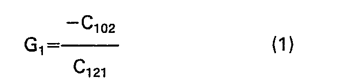
- G1 =the closed loop gain of
operational amplifier 150; - C102=the capacitance of
capacitor 102; and C121=the effective capacitance ofcapacitor array 121, as determined by the operation of switches 134-2 through 134-N and 135-2 through 135-N. -
Capacitor array 121 comprises a plurality of N capacitors 125-1 through 125-N connected between invertinginput lead 136 andoutput terminal 155 ofoperational amplifier 150. Capacitors 125-2 through 125-N ofcapacitor array 121 are selectively connected in parallel with capacitor 125-1 by the operation of appropriate switches 134-2 through 134-N and 135-2 through 135-N. For example, capacitor 125-2 is connected in parallel with capacitor 125-1 when switches 134-2 and 135-2 are closed, and is disconnected when switches 134-2 and 135-2 are open. - The capacitors 125-1 through 125-N in
capacitor array 121 may be equally weighted, such that the capacitance ofcapacitor array 121 connected betweenoutput terminal 155 andlead 136 may be selected in accordance with the following equation:
- C121=the effective capacitance of
capacitor array 121 connected betweenoutput terminal 155 and invertinginput lead 136; - J =is a selected integer ranging from 1 to N equal to the number of capacitors of
capacitor array 121 which are connected betweenoutput terminal 155 and invertinginput lead 136; and - C, =the capacitance of each capacitor 125-1 through 125-N within
capacitor array 121. - CM=the capacitance of the Mth capacitor; and
- Ci=the capacitance of capacitor 125-1, which serves as the first capacitor.
- The effective capacitance of binary
weighted array 121 is equal to
capacitor array 121. - The capacitance values of capacitors 125-1 through 125-N of
capacitor array 121 may also be selected in accordance with any other desired weighting scheme including, but not limited to, weighting schemes which allow companding in accordance with the well known p255 law specified by documents available from the International Telegraph and Telephone Consultative Committee (CCITT) (Europe) and by the American Telephone and Telegraph Company (AT&T) (USA). - The switches within
capacitor array 121 are controlled by thecounter 200 in order to select the desired closed loop ofoperational amplifier 150, as will be more fully described later. - The output signal available on
output terminal 155 ofoperational amplifier 150 is rectified bydiode bridge 156 and alternately integrated with a reference voltage Vref inintegrator stage 300.Rectifier bridge 156 may be replaced with any suitable rectifying means, including a half-wave rectifier comprising a single diode. However, the magnitude of reference voltage Vref must be decreased by approximately 50% if half-wave rectification of output signal Vo is used in place of full-wave rectification.Integrator 300 comprisesoperational amplifier 170, integratingcapacitor 174, andswitches - Diodes can be fabricated MOS devices, but one terminal of the diode is connected to a supply voltage. Alternatively, transistors may be used in place of the diodes, but transistors have current gain. The circuit of Figure 5 may be used in place of bridge rectifier 156 (Fig. 1) to rectify the output signal from
operational amplifier 150 for application tocapacitor 160.Input terminal 700 of rectifier means 699 is connected tonode 700 of Figure 1, andoutputterminal 701 ofrectifier 699 is connected tonode 701 of the circuit of Figure 1.Node 702 of the circuit of Figure 1 is connected to ground whenrectifier 699 is utilized. -
Rectifier 699 comprisesoperational amplifier 702, having its inverted input terminal connected to ground, and its non-inverting input terminal connected to input terminal 700. Thus,operational amplifier 702 functions as a voltage comparator and provides a positive output signal when the input signal applied toterminal 700 is positive. On the other hand,operational amplifier 702 provides a negative output signal when the signal applied toterminal 700 is negative. Operational amplifier 705 has its non-inverting input lead connected to ground, and its inverting input lead connected to input terminal 700 throughresistor 703. Negative feedback is provided between the output lead of operational amplifier 705 and the inverting input lead of operational amplifier 705 byresistor 704. Thus, operational amplifier 705 provides on its output lead a voltage of polarity opposite to the voltage Vo applied toterminal 700.Operational amplifier 706, having its inverting input lead connected to its output lead, and its non-inverting input lead connected toterminal 700, serves as a unity-gain amplifier, thus providing a voltage on its output lead which is of the same polarity as the voltage applied toterminal 700. - Transmission gates 708 (comprising N-Channel MOSFET 708a and P-
Channel MOSFET 708b) and 709 (comprising N-Channel MOSFET 709a and P-Channel MOSFET 709b serve to couple the desired voltage from the output leads ofoperational amplifiers 705 and 706 tooutput terminal 701 ofrectifier 699. For example, when the voltage Vo (Figure 1) applied toterminal 700 is positive,operational amplifier 702 provides a positive voltage on its output lead which is applied to the gates of P-Channel MOSFET 708b and N-Channel MOSFET 709a, thus turning offMOSFET 708b and turning onMOSFET 709a. At the same time, the positive voltage provided on the output lead ofoperational amplifier 702 is inverted byinverter 707, thus providing a negative voltage on the gates of N-Channel MOSFET 708a and P-Channel MOSFET 709b, thus turning off transistor 708a and turning on transistor 709b. Thus, with a positive input signal onterminal 700,transmission gate 708 is turned off andtransmission gate 709 is turned on, thus connecting the positive voltage fromunit gain amplifier 706 toterminal 701. On the other hand, with a negative voltage Vo applied to theinput terminal 700,operational amplifier 702 provides a negative voltage on its output lead, thus causingtransmission gate 708 to turn on andtransmission gate 709 to turn off. Thus, the voltage available on the output lead of operational amplifier 705, which is of opposite polarity to the input voltage applied toterminal 700, and, therefore, a positive voltage, is made available onoutput terminal 701. In this manner, the rectifier means 699 of Figure 5 operates to rectify the input voltage applied to itsterminal 700 and provides the rectified voltage on itsoutput terminal 701. -
Integrator stage 300 is initialized during power- up of the device, by closingswitches opening switch 175, thus dischargingcapacitor 174 to (Voff-0), where Voff is the inherent offset voltage ofoperational amplifier 170.Switches capacitor 174 to zero. - During each integration cycle, the rectified AGC signal is first integrated, followed by the integration of reference voltage Vret. During the first half of each integration cycle, the output signal from
terminal 155 is rectified by rectifier means 156.Switches capacitor 160 between nodes 156-3 and 156-4 of rectifier means 156. Thus during the first half of each integration cycle a positive voltage equal in magnitude to the output voltage Vo is stored oncapacitor 160. Then, during the second half of each integration cycle, switches 161 and 163 open and switches 162 and 164 close, thus connectingcapacitor 160 between invertinginput lead 171 ofoperational amplifier 170 and reference voltage Vref- Vret is a negative voltage. Becausenon-inverting input lead 172 ofoperational amplifier 170 is grounded, invertinginput lead 171 is forced to ground potential. Thus,capacitor 160 is charged to (0-Vref), thus integrating (-V,.ef-Vo) onintegrator stage 300. The output voltage available onnode 177 ofintegrator stage 300 is thus equal G2 (-Vref-Vo), with
- G2 =the closed loop gain of
integrator state 300; - C160=the
capacitcance 160; and - C174=the capacitance of
capacitor 174. - The output voltage of
amplifier 170 appearing onnode 177 is connected tocomparator 180, and compared with ground. The output voltage onoutput lead 190 ofcomparator 180 provides a sign bit of the output signal fromintegrator 300. Thus, if the output voltage ofintegrator stage 300 is positive, the sign bit ofcomparator 180 will be a logical one, and if the output voltage fromintegrator stage 300 is negative, the sign bit fromcomparator 180 will be a logical zero. The sign bit is stored inlatch 191, and controls the operation ofcounter 200. If the sign bit stored inlatch 191 is a logical zero, counter will increase its count by one. On the other hand, if the sign bit stored inlatch 191 is a logical one, thecounter 200 will decrease its count by one. -
Counter 200 contains P bits, available on output leads Oo, 01, 02 ... Op. The state of each bit (logical 1 or logical 0) ofcounter 200 control switches incapacitor array 121, thereby controlling the effective capacitance ofcapacitor array 121. Thus, when counter 200 increases its count, corresponding to receipt of a sign bit which is a logical zero, corresponding to an output voltage Vo which, when rectified by rectifier means 156, is greater in magnitude than the reference voltage Vref, selected capacitors incapacitor array 121 are connected in parallel with capacitor 125-1 by the operation of switches 134-2 through 134-N and 135-2 through 135-N, thus increasing the ratio of capacitance ofarray 121 to the capacitance ofcapacitor 102, thereby decreasing the closed loop gain ofoperational amplifier 150, thereby decreasing the amplitude of output voltage Vo available onoutput terminal 155. As the count provided bycounter 200 increases in value, the effective capacitance ofcapacitor array 121 increases. Therefore, it is preferred that the capacitor ofcapacitor array 121 having the highest capacitance value (capacitor 125-N) be controlled by the most significant bit (Op) ofcounter 200, the next largest capacitance value (capacitor 125-(N-1)) be controlled by the next most significant bit (Op-i), etc., and the smallest capacitance value (125-2) be controlled by the least significant bit (02). Thus, switches 134-1 and 135-1 close in response to bit 01 ofcounter 200 being a logical one, and open in response to bit O1 being a logical zero, where I is an integer ranging from 2 to N. - In a similar fashion, when the count stored in
counter 200 decreases, corresponding to receipt of a sign bit which is a logical one, corresponding to an output voltage Vo which, when rectified by rectifier means 156, is lower in magnitude than the reference voltage Vref, selected capacitors ofcapacitor array 121 are disconnected, thus decreasing the effective capacitance ofcapacitor array 121 connected between invertinginput lead 136 andoutput terminal 155 ofoperational amplifier 150, thus increasing the closed loop gain ofoperational amplifier 150. - When the AGC circuit of this invention has stabilized, thereby providing an output signal Vo on
output terminal 155 which, when rectified, is essentially equal in magnitude to reference voltage Vref, the sign bit available fromcomparator 180 will toggle positive and negative during alternate integration cycles, thus causing counter 200 to toggle up one count and down one count during alternate integration cycles. This causes the closed loop gain ofoperational amplifier 150 to toggle between two neatly equal values, thus providing an essentially constant output voltage Vo onoutput terminal 155, whose amplitude has been controlled by the automatic gain control circuit of this invention. In actual operation, the stabilized output voltage, when rectified, will first be slightly greater in magnitude than the reference voltage Vref, thus causing thecounter 200 to increase its count by one, thus decreasing slightly the closed loop gain ofoperational amplifier 150. Then, the output voltage, when rectified, will be slightly lower in magnitude than the reference voltage Vret, thus causing thecounter 200 to decrease its count by one, thus increasing slightly the closed loop gain ofoperational amplifier 150. Thus, when the AGC circuit of this invention is stabilized, thecounter 200 toggles up one count and down one count on alternate integration cycles. This toggling causes an associated toggling of the closed loop gain ofoperational amplifier 150. However, the change in the closed loop gain ofoperational amplifier 150 due to this single count toggling during stability is sufficiently small as to result in an output signal Vo of substantially constant amplitude. - The switches 110-115, 130-135, 161-164, 173, 175 and 176 may comprise any suitable switch means and, when the invention is utilized to construct an AGC circuit comprising MOSFET elements, preferably comprise single MOSFET devices. The frequency of operation of
switches 161 through 164 (associated with switchedcapacitor 160 and integrator 170) andcounter 200 is capable of being chosen over a wide range of values, depending on the bandwidth of the output signal Vo. In one embodiment, the automatic gain control circuit of this invention is used to control the amplitude of audio signals utilized in a modem, and the frequency of operation of the automatic gain control circuit of this invention is approximately 10 to 100 kilohertz. Of course, other frequencies of operation may be used in accordance with the principles of this invention. - In one embodiment of this invention, three additional least significant bits (0-1, 00, 0, not shown) are provided by
counter 200 which are not utilized in controlling switches withincapacitor array operational amplifier 150 due to noise effects. In this embodiment thecounter 200 must count down eight counts in order to increase the closed loop gain ofoperational amplifier 150, and thus increase the amplitude of the output voltage Vout. Similarly, thecounter 200 must count up eight counts in order to decrease the closed loop gain ofoperational amplifier 150, and thus decrease the amplitude of the output voltage Vout. Thus, transient noise effects on the output signal Vo will have minimal effect on the closed loop gain ofoperational amplifier 150, thereby preventing undesired changes in the amplitude of the output signal Vo in response to short duration transient noise signals. - In another embodiment of this invention, as shown in Figure 2, the closed loop gain of
operational amplifier 150 is determined by the effective capacitance ofcapacitor array 101, connected betweeninput terminal 100 and invertinginput lead 136 ofoperational amplifier 150, andcapacitor 125, connected between invertinginput lead 136 andoutput terminal 155.Capacitor array 101 comprises capacitor 102-1 (having capacitance value Cl) and capacitors 102-2 through 102-N which are selectively connected in parallel with capacitor 102-1 by the operation of switches 110-2 through 110-N and 111-2 through 111-N. In the embodiment of this invention shown in Figure 2, the closed loop gain G, ofoperational amplifier 150 is equal to
operational amplifier 150; - C101 equals the effective capacitance of
capacitor array 101, as determined by the operation of switches 110-2 through 110-N and 111-2 through 111-N; and - C125 equals the capacitance of
capacitor 125. - The capacitors 102-1 through 102-N and
capacitor 101 may utilize any weighting scheme desired, including but not limited to the weighting schemes discussed above forcapacitor array 121 of Figure 1. Thus, capacitors.102-1 through 102-N may be equally weighted, binary weighted, weighted in accordance with the µ255 law, or . weighted in other manners. - As in the operation of capacitor array 121 (Figure 1), the switches 110-2 through 110-N and 111-2 through 111-N of capacitor array 102 (Figure 2) are controlled by the output bits O2 through ON of
counter 200. However, because the capacitance ofcapacitor array 101 forms the numerator of the closed loop gain G1 in the circuit of Figure 2, as opposed to the capacitance ofarray 121 forming the denominator of the closed loop gain (equation 1) of the circuit of Figure 1, the switches ofarray 101 operate in inverse fashion as the switches ofarray 121. Thus, when counter 200 increases its count, corresponding to the receipt of a sign bit which is logical 0, corresponding to an output voltage Vo which, when rectified by rectifier means 156, is greater in magnitude than the reference voltage Vref, selected capacitors incapacitor array 101 are disconnected from capacitor 102-1 by the operation of switches 110-2 through 110-N and 111-2 through 111-N, thus increasing the ratio of capacitance ofcapacitor 125 to the capacitance ofarray 101, thereby decreasing the closed loop gain ofoperational amplifier 150, thereby decreasing the amplitude of output voltage Vo available onoutput terminal 155. As the count provided bycounter 200 increases in value the effective capacitance ofcapacitor array 101 decreases. Therefore, it is preferred that the capacitor ofcapacitor array 101 having the highest capacitance value be controlled by the most significant bit ofcounter 200, the next largest capacitance value be controlled by the next most significant bit., etc., and the smallest capacitance value ofarray 101 be controlled by a least significant bit ofcounter 200. Thus, switch 110-1 and 111-I open in response to a bit 0, ofcounter 200 being a logical one, and close in response to a bit O1 being a logical 0, where L is an integer ranging from 2 to N. - In a similar fashion, when the count stored in
counter 200 decreases, corresponding to receipt of a sign bit which is a logical one, corresponding to an output voltage Vo which, when rectified by rectifier means 156, is lower in magnitude than reference voltage Vref, selected capacitors ofcapacitor array 101 are connected in parallel with capacitor 102-1, thus increasing the effective capacitance ofcapacitor array 101, thus increasing the closed loop gain ofoperational amplifier 150. - Yet another embodiment of this invention, shown in the schematic diagram of Figure 3, utilizes
capacitor array 121 as in the circuit of Figure 1, in conjunction withcapacitor array 101, as in the circuit of Figure 2. Because the operation ofcapacitor arrays - In general, the response time of an automatic gain control circuit is defined as the time constant TAGC of the envelope of the output signal of the automatic gain control circuit, as shown in figure 4b. Figure 4a shows an input signal to an automatic gain control circuit. Figure 4b shows the output signal of the automatic gain control circuit provided in response to the input signal of Figure 4a. The time constant T of the envelope defines the response time of the automatic gain control circuit. Generally, a response time on the order of tens of microseconds is deemed a "fast" AGC response time, and a response time on the order of hundreds of milliseconds is deemed a "slow" AGC response time.
- The response time TAGC of the automatic gain control circuit of this invention is proportional to the time constant T300 of
integrator circuit 300. The time constant ofintegrator circuit 300 is defined as
- T300=The time constant of
integrator stage 300 and thus the response time of the AGC circuit of this invention; - R160=The effective resistance of switched capacitor resistor equivalent 160; and
- C174=The capacitance of
capacitor 174. - The use of switched capacitors as resistor equivalents is described, for example, by Caves et al, in an article "Sample Analog Filtering Using Switched Capacitors as Resistor Equivalents", IEEE Journal of Solid-State Circuits, Vol. SC-12, No. 6, December 1977. The effective resistance of a switched capacitor resistor equivalent (capacitor 160) is equal to

- T160=The switching rate of switched
capacitor 160; and - C,60=The capacitance of
capacitor 160. - From equations (7) and (8), the time constant T300 of
integrator stage 300 follows the following proportionality:
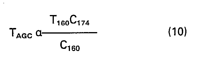
- Thus, the time constant of
integrator stage 300, and thus the response time will be AGC circuit of this invention, may be increased by either increasing the switching speed ofintegrator stage 300, increasing the capacitance ofcapacitor 174, decreasing the capacitance ofcapacitor 160, or a combination of these three techniques. By replacingcapacitor 160 andcapacitor 174 with capacitor arrays (not shown) wherein the effective capacitance ofcapacitor array 160 andcapacitor array 174 may be controlled by switches in a manner similar to the operation ofcapacitor arrays integrator stage 300, and thus the response time of the AGC circuit of this invention, may be controlled over a wide range, as desired. - The response time of the AGC circuit of this invention may also be adjusted by changing the number of least significant bits of
counter 200 which are not used to control the switches ofcapacitor arrays capacitor arrays - While this specification illustrates several embodiments of this invention, it is not to be interpreted as limiting the scope of the invention. Many embodiments of this invention are possible to those skilled in the art in accordance with the teachings of this specification. For example, components other than capacitors may be utilized to control the closed loop gain of the AGC circuit of this invention.
Alternatively, the capacitors of
Claims (8)
whereby the output signal present on said output terminal (701) is equal to the rectified input signal.
Applications Claiming Priority (2)
| Application Number | Priority Date | Filing Date | Title |
|---|---|---|---|
| US06/310,160 US4441082A (en) | 1981-10-09 | 1981-10-09 | Switched capacitor automatic gain control loop |
| US310160 | 1981-10-09 |
Publications (2)
| Publication Number | Publication Date |
|---|---|
| EP0077266A1 EP0077266A1 (en) | 1983-04-20 |
| EP0077266B1 true EP0077266B1 (en) | 1986-01-08 |
Family
ID=23201256
Family Applications (1)
| Application Number | Title | Priority Date | Filing Date |
|---|---|---|---|
| EP82401843A Expired EP0077266B1 (en) | 1981-10-09 | 1982-10-07 | Switched capacitor automatic gain control loop |
Country Status (5)
| Country | Link |
|---|---|
| US (1) | US4441082A (en) |
| EP (1) | EP0077266B1 (en) |
| JP (1) | JPH0691391B2 (en) |
| CA (1) | CA1203292A (en) |
| DE (1) | DE3268443D1 (en) |
Families Citing this family (24)
| Publication number | Priority date | Publication date | Assignee | Title |
|---|---|---|---|---|
| US4555668A (en) * | 1983-10-14 | 1985-11-26 | American Microsystems, Inc. | Gain amplifier |
| US4554508A (en) * | 1983-12-07 | 1985-11-19 | American Microsystems, Incorporated | Carrier detection circuit |
| US4634997A (en) * | 1984-11-13 | 1987-01-06 | At&T Bell Laboratories | Automatic gain control amplifier circuit |
| US4691172A (en) * | 1985-09-10 | 1987-09-01 | Silicon Systems, Inc. | MOS Switched capacitor automatic gain control circuit |
| US4873492A (en) * | 1988-12-05 | 1989-10-10 | American Telephone And Telegraph Company, At&T Bell Laboratories | Amplifier with modulated resistor gain control |
| FI88562C (en) * | 1989-09-19 | 1993-05-25 | Nokia Mobile Phones Ltd | Integrated operating voltage independent dynamic amplitude limiter |
| JP3086512B2 (en) * | 1990-11-14 | 2000-09-11 | エリクソン−ジーイー モービル コミュニケーションズ ホールディング インコーポレイテッド | Transmitter and its power amplifier circuit |
| US5363055A (en) * | 1993-03-15 | 1994-11-08 | General Electric Company | Photodiode preamplifier with programmable gain amplification |
| US6020785A (en) * | 1998-10-23 | 2000-02-01 | Maxim Integrated Products, Inc. | Fixed gain operational amplifiers |
| WO2000038316A1 (en) * | 1998-12-22 | 2000-06-29 | Koninklijke Philips Electronics N.V. | Computer tomograph with a multi-stage charge-integrated read amplifier |
| US6288669B1 (en) | 1999-07-15 | 2001-09-11 | Daramana G. Gata | Switched capacitor programmable gain and attenuation amplifier circuit |
| US6539524B1 (en) * | 2000-05-10 | 2003-03-25 | Agere Systems Inc. | Method and apparatus for matching capacitance of filters having different circuit topologies |
| US7616052B1 (en) * | 2003-03-04 | 2009-11-10 | National Semicondcutor Corporation | Fast adapting filter |
| US7307572B2 (en) * | 2005-06-15 | 2007-12-11 | Freescale Semiconductor, Inc. | Programmable dual input switched-capacitor gain stage |
| US7365597B2 (en) * | 2005-08-19 | 2008-04-29 | Micron Technology, Inc. | Switched capacitor amplifier with higher gain and improved closed-loop gain accuracy |
| US7649957B2 (en) * | 2006-03-22 | 2010-01-19 | Freescale Semiconductor, Inc. | Non-overlapping multi-stage clock generator system |
| CN101355347B (en) * | 2007-07-25 | 2010-07-21 | 盛群半导体股份有限公司 | Linear Programmable Switched Capacitor Gain Amplifier |
| EP2367366B1 (en) * | 2010-03-17 | 2012-11-14 | Nxp B.V. | Control of a microphone |
| JP5429207B2 (en) * | 2010-09-08 | 2014-02-26 | 株式会社デンソー | Capacitive physical quantity detector |
| EP2667156B1 (en) * | 2012-05-25 | 2015-10-21 | Nxp B.V. | Capacitive position sensor system |
| EP2717136B1 (en) | 2012-10-02 | 2017-07-12 | Nxp B.V. | Capacitive position sensor system |
| CN103248330B (en) * | 2013-01-31 | 2015-10-21 | 南京邮电大学 | A kind of programmable gain amplifier of high-gain precision |
| US9438192B2 (en) | 2014-04-01 | 2016-09-06 | Qualcomm Incorporated | Capacitive programmable gain amplifier |
| CN113674670B (en) * | 2021-08-17 | 2024-05-17 | 晟合微电子(肇庆)有限公司 | Driving circuit of display panel and display device |
Family Cites Families (8)
| Publication number | Priority date | Publication date | Assignee | Title |
|---|---|---|---|---|
| GB1342383A (en) * | 1970-08-03 | 1974-01-03 | Marconi Co Ltd | Signal compression and expansion systems |
| GB1513126A (en) * | 1975-04-30 | 1978-06-07 | British Steel Corp | Signal translation circuits |
| JPS5750810Y2 (en) * | 1978-05-30 | 1982-11-06 | ||
| JPS55124315A (en) * | 1979-03-20 | 1980-09-25 | Nec Corp | Automatic gain control circuit |
| JPS5632816A (en) * | 1979-08-28 | 1981-04-02 | Fujitsu Ltd | Variable attenuator |
| GB2059202B (en) * | 1979-09-14 | 1983-11-02 | Plessey Co Ltd | Digitally controlled wide range automatic gain control |
| ZA805415B (en) * | 1979-09-14 | 1981-08-26 | Plessey Overseas | Digitally controlled wide range automatic gain control |
| JPS5658306A (en) * | 1979-10-18 | 1981-05-21 | Nec Corp | Automatic gain control circuit |
-
1981
- 1981-10-09 US US06/310,160 patent/US4441082A/en not_active Expired - Lifetime
-
1982
- 1982-10-07 DE DE8282401843T patent/DE3268443D1/en not_active Expired
- 1982-10-07 EP EP82401843A patent/EP0077266B1/en not_active Expired
- 1982-10-08 JP JP57176429A patent/JPH0691391B2/en not_active Expired - Lifetime
- 1982-10-08 CA CA000413137A patent/CA1203292A/en not_active Expired
Also Published As
| Publication number | Publication date |
|---|---|
| JPH0691391B2 (en) | 1994-11-14 |
| CA1203292A (en) | 1986-04-15 |
| EP0077266A1 (en) | 1983-04-20 |
| DE3268443D1 (en) | 1986-02-20 |
| JPS5875912A (en) | 1983-05-07 |
| US4441082A (en) | 1984-04-03 |
Similar Documents
| Publication | Publication Date | Title |
|---|---|---|
| EP0077266B1 (en) | Switched capacitor automatic gain control loop | |
| US5642075A (en) | Sampled data automatic gain control | |
| CA1270537A (en) | Automatic gain control apparatus | |
| US4598252A (en) | Variable gain power amplifier | |
| Zhak et al. | A low-power wide dynamic range envelope detector | |
| KR100349191B1 (en) | Method and apparatus for converting an analog signal to a digital format | |
| CA1225744A (en) | Voltage comparator circuit | |
| US6492864B2 (en) | Circuit configuration for low-power reference voltage generation | |
| EP0621638B1 (en) | Integrated high voltage differential sensor using the inverse gain of high voltage transistors | |
| US4554508A (en) | Carrier detection circuit | |
| US3931582A (en) | Isolated DC amplifier circuit | |
| EP0514929B1 (en) | Logarithmic intermediate-frequency amplifier | |
| CA1301860C (en) | Circuits with multiple controlled gain elements | |
| US4797569A (en) | Apparatus for pre-defining circuit characteristics | |
| US3562552A (en) | Rms to log converter circuit | |
| US4704545A (en) | Switched capacitor rectifier circuit | |
| US3949294A (en) | Level indicating system | |
| US4692717A (en) | Voltage controlled oscillator with high speed current switching | |
| US4176286A (en) | Signal translator with squelch | |
| JPH0660686A (en) | Semiconductor integrated circuit | |
| CA1196953A (en) | Full wave rectifier having an operational amplifier | |
| CA1036706A (en) | Signal processing system and method | |
| US4317052A (en) | Apparatus for converting an A.C. input signal to a rectified and smoothed D.C. signal | |
| US4950929A (en) | Reducing resistive effects of an electrical switch | |
| US3936720A (en) | Half-wave rectifier circuit |
Legal Events
| Date | Code | Title | Description |
|---|---|---|---|
| PUAI | Public reference made under article 153(3) epc to a published international application that has entered the european phase |
Free format text: ORIGINAL CODE: 0009012 |
|
| AK | Designated contracting states |
Designated state(s): DE FR GB NL SE |
|
| 17P | Request for examination filed |
Effective date: 19830824 |
|
| GRAA | (expected) grant |
Free format text: ORIGINAL CODE: 0009210 |
|
| AK | Designated contracting states |
Designated state(s): DE FR GB NL SE |
|
| REF | Corresponds to: |
Ref document number: 3268443 Country of ref document: DE Date of ref document: 19860220 |
|
| ET | Fr: translation filed | ||
| PLBE | No opposition filed within time limit |
Free format text: ORIGINAL CODE: 0009261 |
|
| STAA | Information on the status of an ep patent application or granted ep patent |
Free format text: STATUS: NO OPPOSITION FILED WITHIN TIME LIMIT |
|
| 26N | No opposition filed | ||
| EAL | Se: european patent in force in sweden |
Ref document number: 82401843.6 |
|
| NLS | Nl: assignments of ep-patents |
Owner name: AMI SPINCO INC., A DELAWARE CORPORATION;AMERICAN M |
|
| NLS | Nl: assignments of ep-patents |
Owner name: AMI SEMICONDUCTOR, INC. |
|
| PGFP | Annual fee paid to national office [announced via postgrant information from national office to epo] |
Ref country code: SE Payment date: 20010920 Year of fee payment: 20 Ref country code: FR Payment date: 20010920 Year of fee payment: 20 Ref country code: DE Payment date: 20010920 Year of fee payment: 20 |
|
| PGFP | Annual fee paid to national office [announced via postgrant information from national office to epo] |
Ref country code: GB Payment date: 20010921 Year of fee payment: 20 |
|
| PGFP | Annual fee paid to national office [announced via postgrant information from national office to epo] |
Ref country code: NL Payment date: 20010925 Year of fee payment: 20 |
|
| REG | Reference to a national code |
Ref country code: FR Ref legal event code: TP Ref country code: FR Ref legal event code: CD |
|
| REG | Reference to a national code |
Ref country code: GB Ref legal event code: IF02 |
|
| REG | Reference to a national code |
Ref country code: FR Ref legal event code: TP |
|
| REG | Reference to a national code |
Ref country code: FR Ref legal event code: TP |
|
| PG25 | Lapsed in a contracting state [announced via postgrant information from national office to epo] |
Ref country code: GB Free format text: LAPSE BECAUSE OF EXPIRATION OF PROTECTION Effective date: 20021006 |
|
| PG25 | Lapsed in a contracting state [announced via postgrant information from national office to epo] |
Ref country code: NL Free format text: LAPSE BECAUSE OF EXPIRATION OF PROTECTION Effective date: 20021007 |
|
| REG | Reference to a national code |
Ref country code: GB Ref legal event code: PE20 Effective date: 20021006 |
|
| EUG | Se: european patent has lapsed |
Ref document number: 82401843.6 |
|
| NLV7 | Nl: ceased due to reaching the maximum lifetime of a patent |
Effective date: 20021007 |