EP0077606A2 - Low or zero insertion force connector for multi-pin arrays - Google Patents
Low or zero insertion force connector for multi-pin arrays Download PDFInfo
- Publication number
- EP0077606A2 EP0077606A2 EP82304749A EP82304749A EP0077606A2 EP 0077606 A2 EP0077606 A2 EP 0077606A2 EP 82304749 A EP82304749 A EP 82304749A EP 82304749 A EP82304749 A EP 82304749A EP 0077606 A2 EP0077606 A2 EP 0077606A2
- Authority
- EP
- European Patent Office
- Prior art keywords
- cam
- plate member
- self
- electrical connector
- cam means
- Prior art date
- Legal status (The legal status is an assumption and is not a legal conclusion. Google has not performed a legal analysis and makes no representation as to the accuracy of the status listed.)
- Granted
Links
- 238000003780 insertion Methods 0.000 title abstract description 18
- 230000037431 insertion Effects 0.000 title abstract description 17
- 238000003491 array Methods 0.000 title abstract description 7
- 230000010354 integration Effects 0.000 abstract description 2
- 230000000694 effects Effects 0.000 abstract 1
- 238000010276 construction Methods 0.000 description 3
- 239000000463 material Substances 0.000 description 3
- ZGHQUYZPMWMLBM-UHFFFAOYSA-N 1,2-dichloro-4-phenylbenzene Chemical compound C1=C(Cl)C(Cl)=CC=C1C1=CC=CC=C1 ZGHQUYZPMWMLBM-UHFFFAOYSA-N 0.000 description 2
- 230000009471 action Effects 0.000 description 2
- 238000005452 bending Methods 0.000 description 2
- 230000008901 benefit Effects 0.000 description 2
- 230000013011 mating Effects 0.000 description 2
- 230000007246 mechanism Effects 0.000 description 2
- 238000000034 method Methods 0.000 description 2
- 239000007787 solid Substances 0.000 description 2
- 229910000906 Bronze Inorganic materials 0.000 description 1
- DMFGNRRURHSENX-UHFFFAOYSA-N beryllium copper Chemical compound [Be].[Cu] DMFGNRRURHSENX-UHFFFAOYSA-N 0.000 description 1
- 239000010974 bronze Substances 0.000 description 1
- 230000006835 compression Effects 0.000 description 1
- 238000007906 compression Methods 0.000 description 1
- 239000004020 conductor Substances 0.000 description 1
- KUNSUQLRTQLHQQ-UHFFFAOYSA-N copper tin Chemical compound [Cu].[Sn] KUNSUQLRTQLHQQ-UHFFFAOYSA-N 0.000 description 1
- 230000001186 cumulative effect Effects 0.000 description 1
- BHEPBYXIRTUNPN-UHFFFAOYSA-N hydridophosphorus(.) (triplet) Chemical compound [PH] BHEPBYXIRTUNPN-UHFFFAOYSA-N 0.000 description 1
- 238000012986 modification Methods 0.000 description 1
- 230000004048 modification Effects 0.000 description 1
- 230000004044 response Effects 0.000 description 1
- 230000000717 retained effect Effects 0.000 description 1
- 238000005476 soldering Methods 0.000 description 1
Images

Classifications
-
- H—ELECTRICITY
- H01—ELECTRIC ELEMENTS
- H01R—ELECTRICALLY-CONDUCTIVE CONNECTIONS; STRUCTURAL ASSOCIATIONS OF A PLURALITY OF MUTUALLY-INSULATED ELECTRICAL CONNECTING ELEMENTS; COUPLING DEVICES; CURRENT COLLECTORS
- H01R12/00—Structural associations of a plurality of mutually-insulated electrical connecting elements, specially adapted for printed circuits, e.g. printed circuit boards [PCB], flat or ribbon cables, or like generally planar structures, e.g. terminal strips, terminal blocks; Coupling devices specially adapted for printed circuits, flat or ribbon cables, or like generally planar structures; Terminals specially adapted for contact with, or insertion into, printed circuits, flat or ribbon cables, or like generally planar structures
- H01R12/70—Coupling devices
- H01R12/82—Coupling devices connected with low or zero insertion force
- H01R12/85—Coupling devices connected with low or zero insertion force contact pressure producing means, contacts activated after insertion of printed circuits or like structures
- H01R12/88—Coupling devices connected with low or zero insertion force contact pressure producing means, contacts activated after insertion of printed circuits or like structures acting manually by rotating or pivoting connector housing parts
Definitions
- the primary object of the present invention is an improved connector for the interconnection of multi-pin arrays to corresponding contacts.
- Tabs 172 and 174 project from the cam plate 158 and slide vertically within slots 128b in the rear wall 128 while tabs 176 and 178 slide vertically within slots 166a in the front wall 166 in cap 168.
- the cap 168 further includes an aperture 169 for receiving the shaft 144 of the pin 142 for external access thereto.
- the cap 168 has apertures 180 and 182 and base 120 has suitably threaded registering bores 184 and 186.
- the base 120, cam actuator 132, cam plate 158 and the cap 168 are made of a suitably rigid plastic material.
Landscapes
- Coupling Device And Connection With Printed Circuit (AREA)
Abstract
Description
- This invention relates generally to electrical connectors and pertains more particularly to connectors of so-called zero or low insertion force type for use with multi-pin arrays.
- The primary advantage in the use of zero insertion force connectors, namely, minimizing loading of interfitting contacts during connection, takes on particularly great significance as the number of contacts simultaneously made increases to levels today seen with circuit components produced by very large scale integration (VLSI) techniques. In this sector, a VLSI device may present a twenty-by-twenty pin array, i.e., a total of four hundred pins, for simultaneous individual mating with collectively supported sockets. The loading forces attending such connection are, of course, cumulative of the force per mating contact pair and can readily amount to a level which may be unattainable for an assembler or not sustainable by support housings of the respective pins and sockets.
- A further problem presented to the connector designer by VLSI is that of readily facilitating connection and disconnection and while minimizing space in which such insertion connection and disconnection are to be effected. Customary practices in the art in larger environs are not applicable. In the above example of VLSI connection, the twenty-by-twenty pin array may be necessary within a square of about two inches per side, i.e., about one-tenth inch pin spacings in both column and row directions. Further connections may envision forty-by-forty pin arrays or more.
- There are generally two types of zero insertion force connectors, one in which the contacts are normally closed and the other in which the contacts are normally open. The present invention relates to a zero or low insertion force connector having normally closed contacts. There are a number of known zero insertion force connectors of the closed-contact type which are used to make connection to conductors on printed circuit boards as well as to the leads of electronic packages or components and which employ camming devices for opening such contacts. Such connectors for printed circuit board connections are shown, for example, in U.S. Patents 4,196,955; 4,159,861; 4,159,154; 3,553,630; 3,426,313 and 3,395,377 and in German Patent 1,118,852. References showing connections to a multi-pin device in a closed contact connector include U.S. Patents 4,080,032 and 4,050,758, the latter reference also being useful in connections to printed circuit boards.
- The primary object of the present invention is an improved connector for the interconnection of multi-pin arrays to corresponding contacts.
- A more particular object of the present invention is to provide such interconnection of the multi- pin/contact arrays with zero or low insertion force.
- In accordance with the invention, an electrical connector has a plurality of contacts having socket terminals disposed in an array corresponding to the multi-pin array and opposite terminals for connection to companion apparatus. The socket terminals are each formed with facing elements thereof closingly biased toward one another to electrically engage a pin to be received therein. Each facing element is defined to-provide a partial boundary surface for the pin upon receipt thereof. A cam is supported for movement in the connector, such cam being adapted for receiving the terminal pins . therein, the cam defining a further partial boundary surface for each terminal pin upon receipt thereof. The cam is movable from one position opposing such closing bias of the contact elements and displacing same to facilitate low-insertion force entry of pins therein to a second position wherein the cam surfaces are inactive in such function and permit self-biased tight engagement of the contact elements with the pins.
- In a particular form of the invention, a cam actuator is provided for moving the cam between its first and second positions, the cam actuator being movable in a direction transverse to the movement of the cam. The cam defines a plurality of openings, one connector contact being situate in each, the openings adapted to receive the terminal pins therein. Each cam opening has a cam surface therein that is movable with the cam to engage the facing contact elements upon movement of the cam to the first position.
- In its particularly preferred embodiment, the cam and cam actuator are plates, the cam plate being movable in an upward direction in response to lateral movement of the cam actuator plate. Both the cam and cam actuator plates comprise cooperating camming surfaces, each including a plurality of successively spaced, inclined cam ramps and slots for effecting movement of the cam between the first and second positions.
-
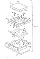
- Fig. 1 is an exploded perspective view of a connector in accordance with the invention and showing both a VLSI device and a companion component to be connected thereby with the VLSI device.
- Fig. 2 is a perspective view of a contact for use in the connector of Fig. 1.
- Figs. 3-5 are respective front, side and top plan elevations of the Fig. 2 contact.
- Fig. 6 is a plan elevation of a segment of the cam plate of the connector of Fig. 1 with one contact seated therein for purposes of explanation.
- Fig. 7 is a partial sectional view of the cam plate of the connector of Fig. 1 as seen from plane VII-VII of Fig. 6.
- Fig. 8 is a partial sectional view of the cam plate of the connector of Fig. 1 as seen from plane VIII-VIII of Fig. 6.
- Fig. 9 is a sectional view as seen from broken plane IX-IX of Fig. 6 with the cam actuating pin, contact, VLSI device, device pin and companion apparatus being shown without sectioning for convenience and simplification of discussion.
- Fig. 10 is a partial sectional view as seen from broken plane X-X of Fig. 6, with the contact, VLSI device, device pin and companion apparatus being shown without sectioning for like convenience and simplification of discussion.
- Fig. 11 is a sectional view, as in Fig. 9, but with the cam plate in operative position, i.e., opposing socket element self-bias and displacing the socket elements to facilitate pin entry in.the socket.
- Fig. 12 is an exploded perspective view of an alternative construction of the connector of the present invention utilizing a different camming mechanism for opening the electrical contacts.
- Fig. 1 depicts
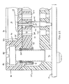
VLSI device 10 andcompanion apparatus 12 for connection thereto, for example, a printed circuit board (PCB). A connector for effecting such interconnection in accordance with the present invention comprises a housing having abase 14, definingcompartment 16 upstanding from base floor 18 and bounded byside walls 20 and 22 andend walls cam plate 28 is shown abovebase 14. Cover orcap 30 of the housing hascompartment 32 upstanding fromcover floor 34 and bounded byside walls end walls wall 44 which extends betweenside wall 36 andend wall 42. For assembly of connector parts,cover 30 has through-bores base 14 has suitably threaded registeringbores cover 30 tobase 14, entrappingcam plate 28 within the housing. -
VLSI device 10 has x-y dimensions compatible with like dimensions ofcompartment 32 ofcover 30, with keying wall 10a orientated compatibly withkeying wall 44 ofcover 30.Pins 62 depend fromundersurface 61 ofVLSI device 10 in an x-y square array, of rows and columns, for example, a twenty-pin by twenty-pin predetermined array having a total of four hundred pins.Contacts 64 are supported inbase 14 in the same array aspins 62 on floor 18. As will be seen in detail in enlarged views below,cam plate 28 has apertures 66 extending therethrough and arranged in the same array as thecontacts 64.Cover 30 similarly includespassages 68 in such array, wherebycontacts 64 may extend throughcam plate 28 andcover 30 to be accessible from the upper exterior of the housing to receivepins 62. -
Cam plate 28 hasend wings detents inserts pin members Cover 30 is provided withopenings members Members ring 85 also being shown in Fig. 9) applied thereto at the undersurface ofcover 30. Upon such assembly ofmembers cover 30 and subsequent fastening ofcover 30 tobase 14, as above discussed, the lower ends ofmembers - As is described in detail below,
members cam plate 28, i.e., by turning the members, the plate may be disposed to confront base floor 18 or to confront the undersurface ofcover 30. - Turning now to Figs. 2-5,
contact 64 has a first terminal 64a which extends throughbase 12 to be accessible below the base for engaging a terminal of companion apparatus, e.g., terminal 64a may be wave soldered to a conductive strip on PCB 12 (Fig. 1). Terminal 64a may also be formed in straight downward configuration for insertion into suitable metallized openings provided inPCB 12 and soldered therein by conventional wave-flow soldering techniques. A second terminal, serving as a pin-receiving socket, is provided opposite such first terminal and is defined by facingelements 64b and 64c which are formed in self-biased preselected attitude to assume generally parallel stance (Fig. 3).Contact 64 is formed of beryllium copper, phosphorous bronze or like material having sufficient resilience to exhibit self-bias, whereby facingelements 64b and 64c will seek to return to such parallel relation, or other preselected self-biased attitude, after release from mutually outward forces thereon opposing such inward self-bias. -
Lances elements 64b and 64c to extend inwardly thereof and preferably have arcuate facing surfaces atends 64d-l and 64e-l. A central support section 64g and an outwardly flared upper pin entry section 64f complete the contact, parts 64f-l and 64f-2 flowing arcuately as shown to define inturned undersurfaces 64f-3 and 64f-4 inboard of facingelements 64b and 64c. - One
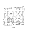
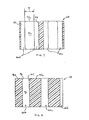
such contact 64 is shown in conjunction withcam plate 28 in Fig. 6, which is a view enlarged approximately twenty times actual size for the two-inch square, twenty-by-twenty array alluded to above. Acontact 64 would, of course, be resident in each of plate apertures 66, but such other contacts are here omitted for convenience and to simplify exposition. The segment ofplate 28 shown in Fig. 6 includes apertures 66a through 66p, each of which has identical outline, as now discussed for aperture 66b. - Considering Figs. 6-8 jointly with Figs. 2-5,
wall 92 and the left side walls ofcam elements right wall 98 and the right side walls ofcam elements contact facing element 64c. Contact lances 64d and 64e are situated in a non-interference path withplate 28, being of expanse less than the spacing across the aperture betweenopposed cam elements space 64h betweencontact facing elements 64b and 64c. Accordingly, ifplate 28 were to be moved forwardly outwardly of the plane of Fig. 6, contact 64 remaining fixed, cam surfaces 94a and 96a would engage contact undersurfaces 64f-3 and 64f-4 and oppose the self-bias of facingelements 64b and 64c to displace same outwardly of each other. - As
cam plate 28 is actually disposed in the plane of Fig. 6, the cam surfaces are inactive, being remote from the cammed contact surfaces 64f-3 and 64f-4, this condition of the connector being further seen in Figs. 9 and 10. Here,member 82 is rotated fully counterclockwise ininsert 78, placingcam plate 28 in its lowermost position, adjacent base floor 18. In such cam inoperative position, contact facing elements exert the full force of contact self-bias uponpin 62 therebetween. - The converse condition of the connector, i.e., cam operative position, is seen in Fig. 11. Here,
member 82 is rotated fully clockwise ininsert 78, placingcam plate 28 in its uppermost position,adjacent cover 30. In such cam operative position, contact self-bias is opposed and contact facing elements are displaced outwardly of one another, bending elastically about the locations of their exit frombase apertures 100.Pin 62 is readily inserted intocontact 64 under this condition and is shown in such seated condition. - The extent of deflection of facing
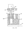
elements 64b and 64c in the cam operative position may be readily established by selection of the width (W in Fig. 7) ofcam elements contacts 62 is established. Thus, while Fig. 11 shows a zero insertion force condition, the contact lances being non-contiguous withpin 62, advantage attends a low, rather than zero, insertion force. Thus, the invention prefers selection of cam element and contact dimensions to provide, in the cam operative position, for the spacing between opposing lance end surfaces from one another to be less than the diameter ofpin 62. The lance end surfaces thus frictionally slidably engagepin 62 upon insertion giving rise to measurable insertion force. The lance end surfaces are preferably arcuate, as noted above. Upon release of the opposing force exerted on the facingcontact elements 64b and 64c by thecam plate 28, thelances - Various modifications to the foregoing disclosed connector will be evident to those skilled in the art and may be introduced without departing from the invention. For example, alternative camming mechanisms may be used to reduce the connector profile or to enhance its strength by resisting bowing, especially in connectors with greater numbers of connections, such as in forty-by-forty pin arrays. Referring to the drawing, Fig. 12 depicts an electronic component such as a VLSI device 110 similar to the
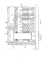
device 10 of Fig. 1 and having a plurality of terminal pins l12 projecting from the undersurface 114 of the device 110 and companion apparatus 116 for connection thereto, for example, a printed circuit board (PCB). An alternative approach for effecting such interconnection in accordance with the present invention includes a connector 118 comprising a housing including a base 120 having a compartment 122 defined by upstanding side walls 124 and 126, end wall 128 and floor 130. The undersurface 131 of the base 120 may include a plurality of longitudinally extending ribs 133 that provide stiffness to the base while permitting a minimal thickness. - A cam actuator 132 is configured in the form of an elongate plate within the base compartment 122 for sliding longitudinal movement relative thereto, as illustrated by the arrow 134. The undersurface 136 of the cam actuator 132 includes a plurality of longitudinally extending, laterally spaced teeth 138 that are adapted to slide within a like plurality of
tracks 140 formed in the base floor 130. Movement of the cam actuator 132 is effected by an actuator pin 142 having a shaft 144 and an eccentric portion 146. The shaft 144 is adapted to be received in an aperture 148 in the base 120 and the eccentric portion 146 is captively retained in an elongate opening 150 provided through a solid portion 132a of the cam actuator 132. The opening 150 is formed to closely receive the eccentric portion 146 such that upon rotation of the pin 142, the - eccentric portion 146 will engage the walls of the cam actuator adjacent the opening 150 and move the cam actuator plate longitudinally relative to the base 120. A slot 143 is provided in the upper surface of the pin shaft 144 to receive a screwdriver or like instrument for facilitating rotation of the pin 142. - The cam actuator 132, in its preferred form, includes a plurality of fingers 152 extending longitudinally from the cam actuator solid portion 132a and terminating in free ends 152a. Each of the fingers is laterally spaced by an opening (not shown). The upper surface of each finger 152 is a camming surface and includes thereon a plurality of inclined cam ramps 154 and slots 156, successively spaced in the longitudinal direction and described in more detail hereinbelow. The free ends 152a of the fingers 152 are adapted to be slidably received in corresponding openings 128a provided in the end wall 128 of the base 120 upon movement of the actuator 132.
- A cam plate 158 overlies cam actuator 132, the cam plate 158 adapted to fit within the compartment 122 of base 120 and to move vertically relative thereto as shown by arrow 160. The bottom surface 158a of the cam plate 158 is a camming surface and comprises a plurality of laterally spaced, longitudinally extending rows of inclined cam ramps 162 and slots 164 that are adapted to cooperate with the cam ramps 154 and slots 156 on the cam actuator plate 132. Movement of the cam plate 158 is restricted to the vertical direction by the base end wall 128 and a front wall 166 of a cap 168 that is secured to the base 120 as by screws 170 (only one of which is shown). Tabs 172 and 174 project from the cam plate 158 and slide vertically within slots 128b in the rear wall 128 while tabs 176 and 178 slide vertically within slots 166a in the front wall 166 in cap 168. The cap 168 further includes an aperture 169 for receiving the shaft 144 of the pin 142 for external access thereto. For assembly of the cap 168 to the base 120, the cap 168 has apertures 180 and 182 and base 120 has suitably threaded registering bores 184 and 186. In the preferred form, the base 120, cam actuator 132, cam plate 158 and the cap 168 are made of a suitably rigid plastic material.
- VLSI device 110 has X-Y dimensions compatible with the base 120, base 120 having internal ledges as at 124a and 126a to support the VLSI device 110 in the connector 118. The pins 112 depend from the undersurface 114 of VLSI device 110 in an X-Y square array of rows and columns, for example, a twenty-pin by twenty-pin predetermined array having a total of four hundred pins. A like number of contacts 188 are supported in the base in a like array of apertures 190 provided in the base floor 130. The cam plate 158 has apertures 192 extending therethrough and arranged in the same array as the contacts 188. The contacts 188 project upwardly from the base 120 through the lateral openings (not shown) between the fingers 152 and into the apertures 192 in the cam plate 158. The contacts 188 may receive the terminal pins 112 between their biased facing elements without the lances as described with reference to Figs. 2-5.
- In operation, rotation of the pin 142 provides longitudinal movement of the cam actuator 132 which, in turn, with the cam ramps 162 of the cam plate riding on the cam ramps 154 of the cam actuator provides vertical upward or downward movement of the cam plate 158 within the connector 118. Cam surfaces disposed within the apertures 192, similar to those described with reference to the arrangement in Figs. 6-8 hereinabove, move the contacts to an open position to freely receive the terminal pins 112 therein. Camming plates having such apertures constructed to receive both the contact facing elements and the VLSI terminals while defining partial boundaries about the VLSI pins contribute to the low profile of the connector.
- It should be noted that the connector arrangement as described herein and shown in Fig. 12 places both the cam plate 158 and cam actuator 132 in compression against the bottom floor 130 of the base 120 under the influence of the spring force of the contacts 188. Such construction substantially minimizes the problems of bowing or bending of the cam plate 158 upon movement upward to spread apart the contact elements. As a result, a larger array of pins than in the known art having very close centers in both row and column directions (e.g., 0.1 inch by 0.1 inch) can be accommodated without problems of the strength of the material or the stiffness of the cam plate itself.
- Having described the construction and operation of the connectors herein, it should now be appreciated that multi-pin connections between the pins of a VLSI device and a companion PCB may be readily effected with zero or low insertion force. The particularly described arrangements are intended to be illustrative and not limited thereto. The true scope of the invention is set forth in the following claims.
Claims (10)
Applications Claiming Priority (4)
| Application Number | Priority Date | Filing Date | Title |
|---|---|---|---|
| US06/302,445 US4422703A (en) | 1981-09-15 | 1981-09-15 | Electrical connector for use with multi-pin arrays |
| US302445 | 1981-09-15 | ||
| US401369 | 1982-07-23 | ||
| US06/401,369 US4496205A (en) | 1982-07-23 | 1982-07-23 | Low or zero insertion force connector for multi-pin arrays |
Publications (3)
| Publication Number | Publication Date |
|---|---|
| EP0077606A2 true EP0077606A2 (en) | 1983-04-27 |
| EP0077606A3 EP0077606A3 (en) | 1983-08-24 |
| EP0077606B1 EP0077606B1 (en) | 1987-05-27 |
Family
ID=26972932
Family Applications (1)
| Application Number | Title | Priority Date | Filing Date |
|---|---|---|---|
| EP19820304749 Expired EP0077606B1 (en) | 1981-09-15 | 1982-09-09 | Low or zero insertion force connector for multi-pin arrays |
Country Status (3)
| Country | Link |
|---|---|
| EP (1) | EP0077606B1 (en) |
| CA (1) | CA1175515A (en) |
| DE (1) | DE3276461D1 (en) |
Cited By (2)
| Publication number | Priority date | Publication date | Assignee | Title |
|---|---|---|---|---|
| FR2557380A1 (en) * | 1983-12-27 | 1985-06-28 | Itt | ELECTRIC CONNECTOR ELEMENT |
| US5254012A (en) * | 1992-08-21 | 1993-10-19 | Industrial Technology Research Institute | Zero insertion force socket |
Family Cites Families (3)
| Publication number | Priority date | Publication date | Assignee | Title |
|---|---|---|---|---|
| US3474387A (en) * | 1967-04-13 | 1969-10-21 | Elco Corp | Zero insertion force connector and contact therefor |
| US3569905A (en) * | 1968-11-19 | 1971-03-09 | Ibm | Electrical connector with cam action |
| US3555488A (en) * | 1969-05-08 | 1971-01-12 | Itt | Printed circuit board connector |
-
1982
- 1982-09-08 CA CA000410974A patent/CA1175515A/en not_active Expired
- 1982-09-09 DE DE8282304749T patent/DE3276461D1/en not_active Expired
- 1982-09-09 EP EP19820304749 patent/EP0077606B1/en not_active Expired
Cited By (2)
| Publication number | Priority date | Publication date | Assignee | Title |
|---|---|---|---|---|
| FR2557380A1 (en) * | 1983-12-27 | 1985-06-28 | Itt | ELECTRIC CONNECTOR ELEMENT |
| US5254012A (en) * | 1992-08-21 | 1993-10-19 | Industrial Technology Research Institute | Zero insertion force socket |
Also Published As
| Publication number | Publication date |
|---|---|
| EP0077606A3 (en) | 1983-08-24 |
| CA1175515A (en) | 1984-10-02 |
| DE3276461D1 (en) | 1987-07-02 |
| EP0077606B1 (en) | 1987-05-27 |
Similar Documents
| Publication | Publication Date | Title |
|---|---|---|
| US4422703A (en) | Electrical connector for use with multi-pin arrays | |
| US4480884A (en) | Zero insertion force connector and circuit card assembly | |
| US5713744A (en) | Integrated circuit socket for ball grid array and land grid array lead styles | |
| US5207598A (en) | Edge card connector | |
| US5162002A (en) | Card edge connector assembly | |
| US5221210A (en) | Circuite board connector | |
| US4826446A (en) | Electrical contact pins and assemblies | |
| US4637670A (en) | Dual in-line package carrier assembly | |
| CA1112314A (en) | Electrical socket connector construction | |
| US3320572A (en) | Electrical connector assembly | |
| US6790054B1 (en) | Two-piece right angle contact edge card connector | |
| US7059869B2 (en) | Metal contact LGA socket | |
| JPS6226559B2 (en) | ||
| US7090507B2 (en) | Socket having substrate locking feature | |
| EP0082679A2 (en) | Multi-pin zero insertion force connector | |
| US20030199182A1 (en) | Electrical connector assembly and method of assembling same | |
| EP0122486B1 (en) | Electrical connectors with quasi-terminal pins | |
| US6908328B2 (en) | Electrical connector with accurately secured contacts | |
| US4417779A (en) | PCB-Mountable connector for terminating flat cable | |
| US5632640A (en) | Insert and rotate connector with improved latching means | |
| US7435098B2 (en) | Electrical interconnection between multiple printed circuit boards | |
| US4496205A (en) | Low or zero insertion force connector for multi-pin arrays | |
| US7175462B2 (en) | PGA type IC socket | |
| US4744771A (en) | Fixing structure of contact tails of electrical connector | |
| EP0400378B1 (en) | Circuit panel socket with cloverleaf contact |
Legal Events
| Date | Code | Title | Description |
|---|---|---|---|
| PUAI | Public reference made under article 153(3) epc to a published international application that has entered the european phase |
Free format text: ORIGINAL CODE: 0009012 |
|
| AK | Designated contracting states |
Designated state(s): BE CH DE FR GB IT LI NL SE |
|
| PUAL | Search report despatched |
Free format text: ORIGINAL CODE: 0009013 |
|
| AK | Designated contracting states |
Designated state(s): BE CH DE FR GB IT LI NL SE |
|
| 17P | Request for examination filed |
Effective date: 19840127 |
|
| ITF | It: translation for a ep patent filed | ||
| GRAA | (expected) grant |
Free format text: ORIGINAL CODE: 0009210 |
|
| AK | Designated contracting states |
Kind code of ref document: B1 Designated state(s): BE CH DE FR GB IT LI NL SE |
|
| REF | Corresponds to: |
Ref document number: 3276461 Country of ref document: DE Date of ref document: 19870702 |
|
| PGFP | Annual fee paid to national office [announced via postgrant information from national office to epo] |
Ref country code: NL Payment date: 19870930 Year of fee payment: 6 |
|
| ET | Fr: translation filed | ||
| PLBE | No opposition filed within time limit |
Free format text: ORIGINAL CODE: 0009261 |
|
| STAA | Information on the status of an ep patent application or granted ep patent |
Free format text: STATUS: NO OPPOSITION FILED WITHIN TIME LIMIT |
|
| 26N | No opposition filed | ||
| PG25 | Lapsed in a contracting state [announced via postgrant information from national office to epo] |
Ref country code: GB Effective date: 19880909 |
|
| PG25 | Lapsed in a contracting state [announced via postgrant information from national office to epo] |
Ref country code: SE Effective date: 19880910 |
|
| PG25 | Lapsed in a contracting state [announced via postgrant information from national office to epo] |
Ref country code: LI Effective date: 19880930 Ref country code: CH Effective date: 19880930 Ref country code: BE Effective date: 19880930 |
|
| BERE | Be: lapsed |
Owner name: THOMAS & BETTS CORP. Effective date: 19880930 |
|
| PG25 | Lapsed in a contracting state [announced via postgrant information from national office to epo] |
Ref country code: NL Effective date: 19890401 |
|
| NLV4 | Nl: lapsed or anulled due to non-payment of the annual fee | ||
| PG25 | Lapsed in a contracting state [announced via postgrant information from national office to epo] |
Ref country code: FR Free format text: LAPSE BECAUSE OF NON-PAYMENT OF DUE FEES Effective date: 19890531 |
|
| REG | Reference to a national code |
Ref country code: CH Ref legal event code: PL |
|
| GBPC | Gb: european patent ceased through non-payment of renewal fee | ||
| PG25 | Lapsed in a contracting state [announced via postgrant information from national office to epo] |
Ref country code: DE Effective date: 19890601 |
|
| REG | Reference to a national code |
Ref country code: FR Ref legal event code: ST |
|
| EUG | Se: european patent has lapsed |
Ref document number: 82304749.3 Effective date: 19890712 |