EP0077606B1 - Connecteur à force d'insertion faible ou nulle pour rangées multi-broches - Google Patents
Connecteur à force d'insertion faible ou nulle pour rangées multi-broches Download PDFInfo
- Publication number
- EP0077606B1 EP0077606B1 EP19820304749 EP82304749A EP0077606B1 EP 0077606 B1 EP0077606 B1 EP 0077606B1 EP 19820304749 EP19820304749 EP 19820304749 EP 82304749 A EP82304749 A EP 82304749A EP 0077606 B1 EP0077606 B1 EP 0077606B1
- Authority
- EP
- European Patent Office
- Prior art keywords
- cam
- plate member
- facing elements
- electrical connector
- movement
- Prior art date
- Legal status (The legal status is an assumption and is not a legal conclusion. Google has not performed a legal analysis and makes no representation as to the accuracy of the status listed.)
- Expired
Links
- 238000003780 insertion Methods 0.000 title description 15
- 230000037431 insertion Effects 0.000 title description 15
- 238000003491 array Methods 0.000 title description 5
- 239000000463 material Substances 0.000 description 3
- ZGHQUYZPMWMLBM-UHFFFAOYSA-N 1,2-dichloro-4-phenylbenzene Chemical compound C1=C(Cl)C(Cl)=CC=C1C1=CC=CC=C1 ZGHQUYZPMWMLBM-UHFFFAOYSA-N 0.000 description 2
- 230000009471 action Effects 0.000 description 2
- 238000005452 bending Methods 0.000 description 2
- 230000008901 benefit Effects 0.000 description 2
- 238000010276 construction Methods 0.000 description 2
- 230000013011 mating Effects 0.000 description 2
- 238000000034 method Methods 0.000 description 2
- 239000007787 solid Substances 0.000 description 2
- 229910000906 Bronze Inorganic materials 0.000 description 1
- DMFGNRRURHSENX-UHFFFAOYSA-N beryllium copper Chemical compound [Be].[Cu] DMFGNRRURHSENX-UHFFFAOYSA-N 0.000 description 1
- 239000010974 bronze Substances 0.000 description 1
- 230000006835 compression Effects 0.000 description 1
- 238000007906 compression Methods 0.000 description 1
- 239000004020 conductor Substances 0.000 description 1
- KUNSUQLRTQLHQQ-UHFFFAOYSA-N copper tin Chemical compound [Cu].[Sn] KUNSUQLRTQLHQQ-UHFFFAOYSA-N 0.000 description 1
- 230000001186 cumulative effect Effects 0.000 description 1
- BHEPBYXIRTUNPN-UHFFFAOYSA-N hydridophosphorus(.) (triplet) Chemical compound [PH] BHEPBYXIRTUNPN-UHFFFAOYSA-N 0.000 description 1
- 230000010354 integration Effects 0.000 description 1
- 230000007246 mechanism Effects 0.000 description 1
- 238000012986 modification Methods 0.000 description 1
- 230000004048 modification Effects 0.000 description 1
- 230000004044 response Effects 0.000 description 1
- 230000000717 retained effect Effects 0.000 description 1
- 238000005476 soldering Methods 0.000 description 1
Images


Classifications
-
- H—ELECTRICITY
- H01—ELECTRIC ELEMENTS
- H01R—ELECTRICALLY-CONDUCTIVE CONNECTIONS; STRUCTURAL ASSOCIATIONS OF A PLURALITY OF MUTUALLY-INSULATED ELECTRICAL CONNECTING ELEMENTS; COUPLING DEVICES; CURRENT COLLECTORS
- H01R12/00—Structural associations of a plurality of mutually-insulated electrical connecting elements, specially adapted for printed circuits, e.g. printed circuit boards [PCB], flat or ribbon cables, or like generally planar structures, e.g. terminal strips, terminal blocks; Coupling devices specially adapted for printed circuits, flat or ribbon cables, or like generally planar structures; Terminals specially adapted for contact with, or insertion into, printed circuits, flat or ribbon cables, or like generally planar structures
- H01R12/70—Coupling devices
- H01R12/82—Coupling devices connected with low or zero insertion force
- H01R12/85—Coupling devices connected with low or zero insertion force contact pressure producing means, contacts activated after insertion of printed circuits or like structures
- H01R12/88—Coupling devices connected with low or zero insertion force contact pressure producing means, contacts activated after insertion of printed circuits or like structures acting manually by rotating or pivoting connector housing parts
Definitions
- This invention relates generally to electrical connectors and pertains more particularly to connectors of so-called zero or low insertion force type for use with multi-pin arrays.
- VLSI very large scale integration
- VLSI further problem presented to the connector designer by VLSI is that of readily facilitating connection and disconnection and while minimizing space in which such insertion connection and disconnection are to be effected. Customary practices in the art in larger environs are not applicable.
- the twenty-by-twenty pin array may be necessary within a square of about 50.8 mm (two inches) per side, i.e., about 2.5 mm (one-tenth inch) pin spacings in both column and row directions. Further connections may envision forty-by-forty pin arrays or more.
- the present invention relates to a zero or low insertion force connector having normally closed contacts.
- zero insertion force connectors of the closed-contact type which are used to make connection to conductors on printed circuit boards as well as to the leads of electronic packages or components and which employ camming devices for opening such contacts.
- Such connectors for printed circuit board connections are shown, for example, in US Patent Specification Nos: 4196955; 4159861; 4159154; 3553630; 3426313 and 3395377 and in German Patent Specification No: 1118852.
- References showing connections to a multipin device in a closed contact connector include US Patent Specification Nos: 4080032 and 4050758, the latter reference also being useful in connections to printed circuit boards.
- US Patent Specification No: 3569905 discloses an electrical connector comprising a housing which supports a plurality of contacts having first and second terminals for respective connection with an external circuit and with tabs on a printed circuit board.
- the second terminals have facing elements which are self-biased to define a normally open position for force free insertion of the circuit board tabs.
- Cam means are provided for deflecting the facing elements into a closed position to make mechanical and electrical contact between the facing elements and the circuit board tabs.
- the present invention seeks to provide an improved connector for the interconnection of multi- pin arrays to corresponding contacts with zero or low insertion force.
- an electrical connector has a plurality of contacts having first and second terminals, the second terminals having facing elements which are closingly self-biased towards one another to electrically engage a pin to be received therebetween.
- the connector also has cam means which define a plurality of openings for receiving the second terminals and which has cam surfaces projecting into the openings and located between the facing elements.
- a cam actuator is provided for moving the cam means between its first and second positions, the cam actuator being movable in a direction transverse to the movement of the cam means.
- the cam means and cam actuator are plates, the cam plate being movable in an upward direction in response to lateral movement of the cam actuator plate.
- both the cam means and cam actuator plates comprise co-operating camming surfaces, each including a plurality of successively spaced, inclined cam ramps and slots for effecting movement of the cam means between its first and second positions.
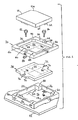
- FIG. 1 depicts VLSI device 10 and companion apparatus 12 for connection thereto, for example, a printed circuit board (PCB).
- a connector for effecting such interconnection in accordance with the present invention comprises a housing having a base 14, defining compartment 16 upstanding from base floor 18 and bounded by side walls 20 and 22 and end walls 24 and 26.
- a cam plate 28 is shown above base 14.
- Cover or cap 30 of the housing has compartment 32 upstanding from cover floor 34 and bounded by side walls 36 and 38, end walls 40 and 42, and keying wall 44 which extends between side wall 36 and end wall 42.
- cover 30 has through-bores 46, 48, 50 and 52 and base 14 has suitably threaded registering bores 54, 56, 58 and 60.
- Fastener bolts (not shown) are passed through bores 46-52 and threaded into bores 54-60 for securing cover 30 to base 14, entrapping cam plate 28 within the housing.
- VLSI device 10 has x-y dimensions compatible with like dimensions of compartment 32 of cover 30, with keying wall 10a oriented compatibly with keying wall 44 of cover 30.
- Pins 62 depend from undersurface 61 of VLSI device 10 in an x-y square array, of rows and columns, for example, a twenty-pin by twenty-pin predetermined array having a total of four hundred pins.
- Contacts 64 are supported in base 14 in the same array as pins 62 on floor 18.
- cam plate 28 has apertures 66 extending therethrough and arranged in the same array as the contacts 64.
- Cover 30 similarly includes passages 68 in such array, whereby contacts 64 may extend through cam plate 28 and cover 30 to be accessible from the upper exterior of the housing to receive pins 62.
- Cam plate 28 has end wings 70 and 72 providing detents 74 and 76 for the retentive seating of inserts 78 and 80. Such inserts each have an interiorly threaded bore for receipt of exteriorly threaded cam actuating pin members 82 and 84.
- Cover 30 is provided with openings 86 and 88 for passage of members 82 and 84 therethrough. Members 82 and 84 are accessible exteriorly of the housing and are secured to cover 30, as by use of snap rings (ring 85 also being shown in Fig. 9) applied thereto at the undersurface of cover 30.
- members 82 and 84 function as position control means for cam plate 28, i.e., by turning the members, the plate may be disposed to confront base floor 18 or to confront the undersurface of cover 30.
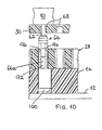
- contact 64 has a first terminal 64a which extends through base 12 to be accessible below the base for engaging a terminal of companion apparatus, e.g., terminal 64a may be wave soldered to a conductive strip on PCB 12 (Fig. 1). Terminal 64a may also be formed in straight downward configuration for insertion into suitable metallized openings provided in PCB 12 and soldered therein by conventional wave- flow soldering techniques.
- a second terminal, serving as a pin-receiving socket, is provided opposite such first terminal and is defined by facing elements 64b and 64c which are formed in self-biased preselected attitude to assume generally parallel stance (Fig. 3).
- Contact 64 is formed by beryllium copper, phosphorous bronze or like material having sufficient resilience to exhibit self-bias, whereby facing elements 64b and 64c will seek to return to such parallel relation, or other preselected self-biased attitude, after release from mutually outward forces thereon opposing such inward self-bias.
- Lances 64d and 64e are struck from elements 64b and 64c to extend inwardly thereof and preferably have arcuate facing surfaces at ends 64d-1 and 64e-1.
- a central support section 64g and an outwardly flared upper pin entry section 64f complete the contact, parts 64f-1 and 64f-2 flowing arcuately as shown to define inturned undersurfaces 64f-3 and 64f-4 inboard of facing elements 64b and 64c.
- FIG. 6 is a view enlarged approximately twenty times actual size for the two-inch square, twenty-by-twenty array alluded to above.
- a contact 64 would, of course, be resident in each of plate apertures 66, but such other contacts are here omitted for convenience and to simplify exposition.
- the segment of plate 28 shown in Fig. 6 includes apertures 66a through 66p, each of which has identical outline, as now discussed for aperture 66b.
- wall 92 and the left side walls of cam elements 94 and 96 provide a residence channel for contact facing element 64b.
- right wall 98 and the right side walls of cam elements 94 and 96 provide a residence channel for contact facing elements 64c.
- Contact lances 64d and 64e are situated in a non-interference path with plate 28, being of expanse less than the spacing across the aperture between opposed cam elements 94 and 96.
- the cam elements extend marginally into the space 64h between contact facing elements 64b and 64c. Accordingly, if plate 28 were to be moved forward out of the plane of Fig. 6, contact 64 remaining fixed, cam surfaces 94a and 96a would engage contact undersurfaces 64f-3 and 64f-4 and oppose the self-bias of facing elements 64b and 64c to displace same outwardly of each other.
- cam plate 28 As cam plate 28 is actually disposed in the plane of Fig. 6, the cam surfaces are inactive, being remote from the cammed contact surfaces 64f-3 and 64f-4, this condition of the connector being further seen in Figs. 9 and 10.
- member 82 is rotated fully counterclockwise in insert 78, placing cam plate 28 in its lowermost position, adjacent base floor 18. In such cam inoperative position, contact facing elements exert the full force of contact self-bias upon pin 62 therebetween.
- cam operative position The converse condition of the connector, i.e., cam operative position, is seen in Fig. 11.
- member 82 is rotated fully clockwise in insert 78, placing cam plate 28 in its uppermost position, adjacent cover 30.
- contact self-bias is opposed and contact facing elements are displaced outwardly of one another, bending elastically about the locations of their exit from base apertures 100.
- Pin 62 is readily inserted into contact 64 under this condition and is shown in such seated condition.
- the extent of deflection of facing elements 64b and 64c in the cam operative position may be readily established by selection of the width (W in Fig. 7) of cam elements 94 and 96, once the configuration of contacts 62 is established.
- W in Fig. 7 shows a zero insertion force condition
- the contact lances being non-contiguous with pin 62
- advantage attends a low, rather than zero, insertion force.
- the invention prefers selection of cam element and contact dimensions to provide, in the cam operative position, for the spacing between opposing lance end surfaces from one another to be less than the diameter of pin 62. The lance end surfaces thus frictionally slidably engage pin 62 upon insertion giving rise to measurable insertion force.
- the lance end surfaces are preferably arcuate, as noted above.
- the lances 64d and 64e under the influence of the self-bias force of the contact, provide a further wiping action as between such arcuate surfaces and the pins.
- the pin wiping action surface oxides may be removed and gas-tight electrical connection readily realized.
- an alternative approach for effecting such interconnection in accordance with the present invention includes a connector comprising a housing including a base having a compartment defined by upstanding side walls, end wall and floor.
- the undersurface of the base may include a plurality of longitudinally extending ribs that provide stiffness to the base while permitting a minimal thickness.
- a cam actuator is configured in the form of an elongate plate within the base compartment for sliding longitudinal movement relative thereto.
- the undersurface of the cam actuator includes a plurality of longitudinally extending, laterally spaced teeth that are adapted to slide within a like plurality of tracks formed in the base floor. Movement of the cam actuator is effected by an actuator pin having a shaft and an eccentric portion.
- the shaft is adapted to be received in an aperture in the base and the eccentric portion is captively retained in an elongate opening provided through a solid portion of the cam actuator.
- the opening is formed to closely receive the eccentric portion such that upon rotation of the pin, the eccentric portion will engage the walls of the cam actuator adjacent the opening and move the cam actuator plate longitudinally relative to the base.
- a slot is provided in the upper surface of the pin shaft to receive a screwdriver or like instrument for facilitating rotation of the pin.
- the cam actuator in its preferred form, includes a plurality of fingers extending longitudinally from the cam actuator solid portion and terminating in free ends. Each of the fingers is laterally spaced by an opening.
- the upper surface of each finger is a camming surface and includes thereon a plurality of inclined cam ramps and slots, successively spaced in the longitudinal direction and described in more detail hereinbelow.
- the free ends of the fingers are adapted to be slidably received in corresponding openings provided in the end wall of the base upon movement of the actuator.
- a cam plate overlies the cam actuator, the cam plate being adapted to fit within the compartment of base and to move vertically relative thereto.
- the bottom surface of the cam plate is a camming surface and comprises a plurality of laterally spaced, longitudinally extending rows of inclined cam ramps and slots that are adapted to cooperate with the cam ramps and slots on the cam actuator plate. Movement of the cam plate is restricted to the vertical direction by the base end wall and a front wall of a cap that is secured to the base as by screws. Tabs project from the cam plate and slide vertically within slots in the rear wall while the tabs slide vertically within slots in the front wall in the cap.
- the cap further includes an aperture for receiving the shaft of the pin for external access thereto.
- the cap has apertures and the base has suitably threaded registering bores.
- the base, cam actuator, cam plate and the cap are made of a suitably rigid plastic material.
- the latter mentioned VLSI device has X-Y dimensions compatible with the base and the base has internal ledges to support the VLSI device in the connector.
- the pins depend from the undersurface of the VLSI device in an X-Y square array of rows and columns, for example, a twenty-pin by twenty-pin predetermined array having a total of four hundred pins.
- a like number of contacts are supported in the base in a like array of apertures provided in the base floor.
- the cam plate has apertures extending therethrough and arranged in the same array as the contacts. The contacts project upwardly from the base through lateral openings between the fingers and into the apertures in the cam plate. The contacts may receive the terminal pins between their biased facing elements without the lances as described with reference to Figs. 2-5.
- rotation of the pin provides longitudinal movement of the cam actuator which, in turn, with the cam ramps of the cam plate riding on the cam ramps of the cam actuator provides vertical upward or downward movement of the cam plate within the connector.
- Cam surfaces disposed within the apertures similar to those described with reference to the arrangement in Figs. 6-8 hereinabove, move the contacts to an open position to freely receive the terminal pins therein.
- Camming plates having such apertures constructed to receive both the contact facing elements and the VLSI terminals while defining partial boundaries about the VLSI pins contribute to the low profile of the connector.
Landscapes
- Coupling Device And Connection With Printed Circuit (AREA)
Claims (8)
caractérisé en ce que lesdites surfaces de cames (94a, 96a) font saillie dans lesdites ouvertures (66) situées entre lesdits éléments en regard (64b, 64c) de manière que lorsque ledit moyen à cames (28) est déplacé dans sa première position, lesdites surfaces de cames (94a, 96a) s'engagent dans des parties internes (64f 1-4) desdits éléments en regard (64b, 64c) et amènent de ce fait lesdits éléments en regard (64b, 64c) à diverger pour permettre auxdites broches (62) d'être facilement reçues dans lesdites secondes bornes; lesdits éléments en regard (64b, 64c) convergeant lorsque ledit moyen à came (28) se déplace dans sa seconde position, ce grâce à quoi lesdits éléments en regard (64b, 64c) peuvent exercer entre eux la totalité de la force de ladite autocontrainte sur les broches (62).
Applications Claiming Priority (4)
| Application Number | Priority Date | Filing Date | Title |
|---|---|---|---|
| US06/302,445 US4422703A (en) | 1981-09-15 | 1981-09-15 | Electrical connector for use with multi-pin arrays |
| US302445 | 1981-09-15 | ||
| US401369 | 1982-07-23 | ||
| US06/401,369 US4496205A (en) | 1982-07-23 | 1982-07-23 | Low or zero insertion force connector for multi-pin arrays |
Publications (3)
| Publication Number | Publication Date |
|---|---|
| EP0077606A2 EP0077606A2 (fr) | 1983-04-27 |
| EP0077606A3 EP0077606A3 (en) | 1983-08-24 |
| EP0077606B1 true EP0077606B1 (fr) | 1987-05-27 |
Family
ID=26972932
Family Applications (1)
| Application Number | Title | Priority Date | Filing Date |
|---|---|---|---|
| EP19820304749 Expired EP0077606B1 (fr) | 1981-09-15 | 1982-09-09 | Connecteur à force d'insertion faible ou nulle pour rangées multi-broches |
Country Status (3)
| Country | Link |
|---|---|
| EP (1) | EP0077606B1 (fr) |
| CA (1) | CA1175515A (fr) |
| DE (1) | DE3276461D1 (fr) |
Families Citing this family (2)
| Publication number | Priority date | Publication date | Assignee | Title |
|---|---|---|---|---|
| US4501461A (en) * | 1983-12-27 | 1985-02-26 | International Telephone And Telegraph Corporation | Zero insertion force socket |
| US5254012A (en) * | 1992-08-21 | 1993-10-19 | Industrial Technology Research Institute | Zero insertion force socket |
Family Cites Families (3)
| Publication number | Priority date | Publication date | Assignee | Title |
|---|---|---|---|---|
| US3474387A (en) * | 1967-04-13 | 1969-10-21 | Elco Corp | Zero insertion force connector and contact therefor |
| US3569905A (en) * | 1968-11-19 | 1971-03-09 | Ibm | Electrical connector with cam action |
| US3555488A (en) * | 1969-05-08 | 1971-01-12 | Itt | Printed circuit board connector |
-
1982
- 1982-09-08 CA CA000410974A patent/CA1175515A/fr not_active Expired
- 1982-09-09 DE DE8282304749T patent/DE3276461D1/de not_active Expired
- 1982-09-09 EP EP19820304749 patent/EP0077606B1/fr not_active Expired
Also Published As
| Publication number | Publication date |
|---|---|
| EP0077606A2 (fr) | 1983-04-27 |
| EP0077606A3 (en) | 1983-08-24 |
| CA1175515A (fr) | 1984-10-02 |
| DE3276461D1 (en) | 1987-07-02 |
Similar Documents
| Publication | Publication Date | Title |
|---|---|---|
| US4422703A (en) | Electrical connector for use with multi-pin arrays | |
| US4826446A (en) | Electrical contact pins and assemblies | |
| EP0349595B1 (fr) | Connecteur plat pour cartes de circuits | |
| EP0443493B1 (fr) | Connecteur électrique avec appareil d'extraction de module | |
| US4480884A (en) | Zero insertion force connector and circuit card assembly | |
| US4637670A (en) | Dual in-line package carrier assembly | |
| US4619495A (en) | High-density press-fit cardedge connectors | |
| US4722704A (en) | High density socket contact receptacle | |
| US5221210A (en) | Circuite board connector | |
| US4033656A (en) | Low profile integrated circuit socket | |
| US4018494A (en) | Interconnection for electrically connecting two vertically stacked electronic packages | |
| US6790054B1 (en) | Two-piece right angle contact edge card connector | |
| US20080182446A1 (en) | Fine pitch electrical connector | |
| US4713020A (en) | Connector unit | |
| US7059869B2 (en) | Metal contact LGA socket | |
| US20030199182A1 (en) | Electrical connector assembly and method of assembling same | |
| EP0122486B1 (fr) | Connecteurs électriques avec des broches quasi-terminales | |
| US6238219B1 (en) | Electrical connection method | |
| US7438556B2 (en) | Electrical interconnection between multiple printed circuit boards | |
| US5632640A (en) | Insert and rotate connector with improved latching means | |
| US7435098B2 (en) | Electrical interconnection between multiple printed circuit boards | |
| US4496205A (en) | Low or zero insertion force connector for multi-pin arrays | |
| US3876274A (en) | Receptacles employing high density array of overlapping self-adjustable contacts | |
| US20050142920A1 (en) | PGA type IC socket | |
| EP0400378B1 (fr) | Socle de panneau de circuit imprimé à contact en forme de trèfle |
Legal Events
| Date | Code | Title | Description |
|---|---|---|---|
| PUAI | Public reference made under article 153(3) epc to a published international application that has entered the european phase |
Free format text: ORIGINAL CODE: 0009012 |
|
| AK | Designated contracting states |
Designated state(s): BE CH DE FR GB IT LI NL SE |
|
| PUAL | Search report despatched |
Free format text: ORIGINAL CODE: 0009013 |
|
| AK | Designated contracting states |
Designated state(s): BE CH DE FR GB IT LI NL SE |
|
| 17P | Request for examination filed |
Effective date: 19840127 |
|
| ITF | It: translation for a ep patent filed | ||
| GRAA | (expected) grant |
Free format text: ORIGINAL CODE: 0009210 |
|
| AK | Designated contracting states |
Kind code of ref document: B1 Designated state(s): BE CH DE FR GB IT LI NL SE |
|
| REF | Corresponds to: |
Ref document number: 3276461 Country of ref document: DE Date of ref document: 19870702 |
|
| PGFP | Annual fee paid to national office [announced via postgrant information from national office to epo] |
Ref country code: NL Payment date: 19870930 Year of fee payment: 6 |
|
| ET | Fr: translation filed | ||
| PLBE | No opposition filed within time limit |
Free format text: ORIGINAL CODE: 0009261 |
|
| STAA | Information on the status of an ep patent application or granted ep patent |
Free format text: STATUS: NO OPPOSITION FILED WITHIN TIME LIMIT |
|
| 26N | No opposition filed | ||
| PG25 | Lapsed in a contracting state [announced via postgrant information from national office to epo] |
Ref country code: GB Effective date: 19880909 |
|
| PG25 | Lapsed in a contracting state [announced via postgrant information from national office to epo] |
Ref country code: SE Effective date: 19880910 |
|
| PG25 | Lapsed in a contracting state [announced via postgrant information from national office to epo] |
Ref country code: LI Effective date: 19880930 Ref country code: CH Effective date: 19880930 Ref country code: BE Effective date: 19880930 |
|
| BERE | Be: lapsed |
Owner name: THOMAS & BETTS CORP. Effective date: 19880930 |
|
| PG25 | Lapsed in a contracting state [announced via postgrant information from national office to epo] |
Ref country code: NL Effective date: 19890401 |
|
| NLV4 | Nl: lapsed or anulled due to non-payment of the annual fee | ||
| PG25 | Lapsed in a contracting state [announced via postgrant information from national office to epo] |
Ref country code: FR Free format text: LAPSE BECAUSE OF NON-PAYMENT OF DUE FEES Effective date: 19890531 |
|
| REG | Reference to a national code |
Ref country code: CH Ref legal event code: PL |
|
| GBPC | Gb: european patent ceased through non-payment of renewal fee | ||
| PG25 | Lapsed in a contracting state [announced via postgrant information from national office to epo] |
Ref country code: DE Effective date: 19890601 |
|
| REG | Reference to a national code |
Ref country code: FR Ref legal event code: ST |
|
| EUG | Se: european patent has lapsed |
Ref document number: 82304749.3 Effective date: 19890712 |