EP0077658A2 - Verfahren und Schaltkreis für eine Tastenfeldabtastung und -schnittstelle - Google Patents
Verfahren und Schaltkreis für eine Tastenfeldabtastung und -schnittstelle Download PDFInfo
- Publication number
- EP0077658A2 EP0077658A2 EP82305496A EP82305496A EP0077658A2 EP 0077658 A2 EP0077658 A2 EP 0077658A2 EP 82305496 A EP82305496 A EP 82305496A EP 82305496 A EP82305496 A EP 82305496A EP 0077658 A2 EP0077658 A2 EP 0077658A2
- Authority
- EP
- European Patent Office
- Prior art keywords
- keys
- keyboard
- memory
- activated
- key
- Prior art date
- Legal status (The legal status is an assumption and is not a legal conclusion. Google has not performed a legal analysis and makes no representation as to the accuracy of the status listed.)
- Withdrawn
Links
- 238000000034 method Methods 0.000 title claims abstract description 25
- 230000015654 memory Effects 0.000 claims abstract description 70
- 238000012545 processing Methods 0.000 claims description 33
- 230000008859 change Effects 0.000 claims description 22
- 230000004913 activation Effects 0.000 claims description 17
- 238000004891 communication Methods 0.000 claims description 7
- 230000005540 biological transmission Effects 0.000 abstract description 26
- 230000000994 depressogenic effect Effects 0.000 abstract description 26
- 230000002093 peripheral effect Effects 0.000 abstract description 3
- 238000012546 transfer Methods 0.000 description 42
- 238000012360 testing method Methods 0.000 description 17
- 238000001994 activation Methods 0.000 description 16
- 230000006870 function Effects 0.000 description 6
- 230000001149 cognitive effect Effects 0.000 description 3
- 238000010586 diagram Methods 0.000 description 3
- 238000012986 modification Methods 0.000 description 3
- 230000004048 modification Effects 0.000 description 3
- 230000008569 process Effects 0.000 description 3
- 230000008901 benefit Effects 0.000 description 2
- 230000008878 coupling Effects 0.000 description 2
- 238000010168 coupling process Methods 0.000 description 2
- 238000005859 coupling reaction Methods 0.000 description 2
- 238000001514 detection method Methods 0.000 description 2
- 230000004044 response Effects 0.000 description 2
- 230000004308 accommodation Effects 0.000 description 1
- 230000003213 activating effect Effects 0.000 description 1
- 230000004075 alteration Effects 0.000 description 1
- 230000001143 conditioned effect Effects 0.000 description 1
- 238000010276 construction Methods 0.000 description 1
- 239000013078 crystal Substances 0.000 description 1
- 230000001351 cycling effect Effects 0.000 description 1
- 238000011161 development Methods 0.000 description 1
- 230000000694 effects Effects 0.000 description 1
- 230000036039 immunity Effects 0.000 description 1
- 238000013507 mapping Methods 0.000 description 1
- 230000005055 memory storage Effects 0.000 description 1
- 230000008520 organization Effects 0.000 description 1
- 238000005070 sampling Methods 0.000 description 1
Images


Classifications
-
- H—ELECTRICITY
- H03—ELECTRONIC CIRCUITRY
- H03M—CODING; DECODING; CODE CONVERSION IN GENERAL
- H03M11/00—Coding in connection with keyboards or like devices, i.e. coding of the position of operated keys
- H03M11/003—Phantom keys detection and prevention
Definitions
- the present invention relates to keyboard communication, and in particular it relates to interface method and circuitry used to scan and to communicate the output of a keyboard to the data input to a data processing system.
- Manually activated keyboards are widely used for entering information into a data processing system.
- a manually activated typewriter-type keyboard has been among the first means by which a human operator has been able to control or otherwise actively interface with the computer system.
- the computer console included a number of toggle switches which could be set or reset to allow the computer operator to communicate special instructions to the computer system without dependence on the keyboard.
- toggle switches and computer consoles were generally arranged and configured as manually settable registers directly addressable through the central processing unit. Later, as systems were developed, it became an advantage to dedicate control keys on a keyboard in place of the toggle switches. But in each case, the dedicated key on the keyboard, like the toggle switches, had a singular significance which could be attributed to it by the operating computer system in which the keyboard was used. For example, in the case of word processors, control keys relating to ordinary typing functions and to particular word processing corrective functions or formatting functions are provided on the keyboard.
- control keys are subject to the limitation and restriction that activation of any one control key cannot be varied by the operator but is fixed by the operating system and that multiple activation of character keys or control keys, which shall be referred to herein as "chording", has no intelligible significance to the operating system.
- the present invention is a method for encoding and communicating keyed input information to a data processing system comprising the steps of scanning a keyboard to detect activated keys. All activated keys detected during a scan of the entire keyboard are memorized. The memorized activated keys are then communicated to the data processing system as a single binary word of arbitrary bit length determined by the number of activated keys detected during the scan of the keyboard. By virtue of this combination of steps, a plurality of keys may be simultaneously activated to generate a binary word of arbitrary length.
- word means a group of bits having a single cognitive meaning, i.e., the representation of a character, a control function, an instruction and the like. The binary word is capable of being associated in a computer system with a meaning which is unrelated to the meaning associated by the computer system with any one of the plurality of keys which is detected as being simultaneously activated during the scan of the keyboard.
- the present invention also includes a keyboard interface circuit coupled to a plurality of keys of a keyboard and to a data processing system which information is communicated from the keyboard.
- the interface circuit comprises a scanning means for addressing the plurality of keys and detecting the activation status of each of the keys.
- a memory means is coupled to the scanning means for storing a representation of the activated keys detected during each addressing of all keys of the keyboard.
- a communication means is coupled to the memory means to selectively interface and transfer the stored representation to the data processing system as a binary word of arbitrary bit length determined by the number of keys detected as being activated during the addressing of all keys of the keyboard.
- the principal object of the present invention is to provide a means and methodology whereby a keyboard input device may be scanned to allow selective significance to be associated with the activation of any given key. Furthermore, an object of the invention is to allow simultaneous activation of a plurality of keys of a keyboard to be represented as a multiple-component binary word of arbitrary bit length having associated therewith an arbitrary meaning not necessarily related to the meaning of any component part of the word.
- the multiple-component word is distinguished as a cognitive entity from its various component parts by setting the most significant bit of each component part to the same selected one of the two permissible binary values, except the most significant bit of the last component part of the multiple-component word, which is set to the other of the two permissible binary values.
- FIGURE 1 shows a manually manipulated keyboard 10 in which keys are depressed to effect key activation, a keyboard control system 11 and an operatively associated data processing system 12.
- Keyboard 10 is illustrated as having its keys organized into a switching array of sixteen rows, XO through X15 and eight columns, YO through Y7.
- Keyboard 10 is constructed according to conventional principles and differs only from other keyboards in the number or significance attached to the keys and not in the particular manner of construction or physical organization of the keys.
- a key is manually depressed by the operator in a scanned row, a signal will occur on the corresponding column output YO-Y7 indicating its activation. If a key is not depressed at a column location of a scanned row, the column output remains inactive.
- Rows XO-X15 are sequentially addressed as described below, so that during any given time period, each of the activated keys in the addressed row will produce an active output signal on the associated column output YO-Y7.
- Keyboard 10 which may be physically housed in a central console, is coupled through a 24-line bus to a dedicated processor 36.
- the cable includes bus 14, coupling rows XO-X15 to multiplexer 16 and an 8-line bus 18 coupling the column output terminals YO-Y7 to the dedicated processor system 36.
- Multiplexer 16 is coupled by a 4-line bus 24 to the output of a counter 22 of the dedicated processor 36.
- Counter 22 provides a series of sixteen 4-bit words at its output beginning at 0000 and ending at llll.
- the series of 4-bit words corresponds to the addresses of the rows XO-X15.
- the counter 22 is sequentially stepped through each of the row addresses in response to commands issued by a CPU 26 included in the dedicated processor system 36 to provide the series of 4-bit words to the multiplexer 16, one at a time. After cycling through the series of sixteen row addresses once, the counter 22 repeats the sixteen row address sequence.
- Multiplexer 16 decodes the 4-bit address generated by counter 22 to selectively activate each of the rows XO-X15 in sequence.
- Multiplexer 16 activates the addressed row by applying a voltage to one of the sixteen lines, XO-X15, according to the count received from counter 22.
- the binary word 0000 generated by counter 22 and coupled to multiplexer 16 causes a row-activating voltage to be applied to the line associated with row XO, thereby, activating or selecting that row.
- Multiplexer maintains all other lines associated with the other row addresses Xl-X15 at ground potential, or inactivated.
- the binary word 0001 causes multiplexer 16 to activate row Xl and so forth until the binary word 1111 causes activation of row X15 at the end of one row scanning sequence.
- the voltage applied to the selected row by the multiplexer 16 is coupled to the corresponding column output line through a switch which is closed by depression of the key.
- the column output line corresponding to each depressed key in the addressed row will be activated.
- the column output line corresponding to each position of an undepressed or "up" key does not receive a voltage.
- the eight column output lines YO-Y7 provide an 8-bit binary signal that signifies the ke depression status of the eight keys contained in each addressed row.
- This 8-bit column output signal is coupled by bus 18 to the CPU 26 of the dedicated processor system 36.
- the CPU 26 also receives an input from the row-a ⁇ dress counter 22 over line 23 indicative of the 4-bit row address output sent to the multiplexer 16 resulting in the generation of the 8-bit column output signal.
- CPU 2£ is provided
- CPU 26 responds to each column output signal by comparing the key depression status of each key represented by that signal with the key depression status of the same key existing at the time the same row was addressed during the immediately previous keyboard scan cycle. If a change in the key depression status has occurred in the row since it was addressed during the previous keyboard scan cycle, i.e., a previously undepressed key is depressed or a previously depressed key is released, a difference in the key depression status is detected.
- the data processing system 12 includes a pair of memories, namely, map memory 2E and ring buffer memory 30, that cooperate with the CPU 26 in the execution of the aforedescribed comparison, storage and transmission of new key depression status.
- Counter 22 is controlled by and is coupled to a dedicated CPU 26 for purposes of timing synchronization and communication by line 23.
- CPU 26 in turn is coupled to map and ring buffer memories 28 and 30 through conventional control lines 32 and a data address bus 34.
- map and ring buffer memories 28 and 30 through conventional control lines 32 and a data address bus 34.
- a conventional, firmware-programmed 8048 microcomputer chip is employed in the preferred embodiment as dedicated processor system 36.
- the component parts of processor system 36 have been separately illustrated and described in FIGURE 1 only for the purposes of illustration and for clarity of understanding of the methodology of the present invention. The component description shown in FIGURE 1 is not to be taken as a restriction or limitation of the scope of the present invention.
- multiplexer 16 and counter 22 are shown as separate elements, they may, in fact, be designated portions of the general microcomputer circuitry within the 8048 chip formed by any means well known in the art, such as by a combination of firmware-programmed memory and registers.
- map and ring buffer memories 28 and 30 are shown as separate memories when, in fact, they may be separately designated portions of a single physical memory, which may further be combined on the same integrated circuit chip with CPU 26 as they are in the 8048 microprocessor.
- CPU 26 includes additional memory, not separately shown, for other program storage and other general uses.
- CPU 26 of dedicated processor system 36 has a serial data output line 38 and a serial data input line 40.
- the clock rate of CPU 26 is controlled by a conventional crystal 42, whereby dedicated processor system 36 runs independently of and asynchronously with respect to data processing system 12.
- Dedicated processor system 36 and data processing system 12 communicate via data output line 38 and input line 40. The communication is coordinated through a conventional interrupt timing scheme executed by the CPU 26.
- Data input line 40 is coupled to a buffer circuit 42 which includes a Schmitt trigger inverter, whose hysteresis improves noise immunity.
- Data output line 38 is similarly coupled to a buffer 44 which includes an open- collector TTL gate in combination with a pullup resistor to provide a voltage compatible signal to the data processing system 12.
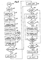
- FIGURE 2 illustrates the scanning method implemented by the circuitry of FIGURE 1 during its asynchronous and independent operation from a computer operating system type data processing system 12.
- Map memory 28 which stores representations of the depression status of the keys of keyboard 10, is initialized at step 50 to contain key up status representations for all keys.
- Ring buffer memory 30, which stores a transmission key code representation of each key depression status to be transmitted by the dedicated processor system 36 to the computer operating system 12, is emptied at step 52.
- An interrupt timer within processor system 36 in actuality a register or memory location controlled by CPU 26, is initialized and started. The interrupt timer cyclically counts down through a programmably determined interval to periodically test for a data transfer condition.
- the interrupt timer periodically interrupts the keyboard scanning operation executed by the CPU 26 and causes the CPU 26 to execute a data transfer interrupt operation.
- Processor system 36 has two settable flags or bit registers whose status determine the execution of steps of the keyboard scanning operation. The first flag is the output flag, which is cleared at step 56, and the second flag is the difference flag, which is cleared at step 58. The significance and function of each of these flags is described hereinafter in further detail.
- step 60 the counter 22 is commanded by CPU 26 to issue the address of the next row to be interrogated for key depressions.
- a new or "next" row is addressed approximately every one-half millisecond.
- CPU receives a unique pair of numbers, one from counter 22 and one from bus 18, which together indicate the specific row which has been addressed by counter 22 and the depression status of the keys in that row at the time of its addressing.
- Each key has a unique row and column number pair associated with it.
- Map memory 28 forms a conceptual mirror image of the keys within keyboard 10.
- Map memory 28 has storage locations in an array of rows and columns which have a one-to-one mapping with the keys of keyboard 10. Each storage location in memory map 28 is a one bit cell. Initially, a binary value, one in the preferred embodiment, corresponding to a key up status condition is loaded into each cell at step 50.
- the storage locations in map memory 28 and rows of keyboard 10 are synchronously addressed by CPU 26 as keyboard 10 is scanned.
- the contents of each addressed row of cells in map memory 28 are compared against the column output signal received over bus 18 in response to the addressing of the corresponding row of keys in keyboard 10.
- the comparison is tested for a difference.
- the difference flag is set at step 66 and the map memory 28 is updated at step 68 by loading into the map memory a new set of binary values corresponding to the compared column output signal.
- the new set of binary values are loaded at the addressed memory storage locations corresponding to the addressed row in the keyboard 10 containing the detected different key depression status.
- Setting the difference flag signifies the occurrence of a change in the key depression status between successive scans of the keyboard 10 and, as will be described in further detail hereinafter with reference to FIGURE 3, prepares the dedicated processor system 36 to condition itself to output new key depression status of the keyboard resulting from the change.
- the difference flag is set only one time for each scan of the keyboard 10. However, there may be changes in the key depression status in more than one row of the keyboard, each of which would require an updating of the map memory 28. Thus, the difference test at step 64 is executed for each addressed row of the keyboard 10 and the map memory 28 is updated at step 68 whenever a difference is detected regardless of whether difference flag has been previously set.
- the output flag is set at the end of each scan of the entire keyboard 10 whenever at least one key depression status change is detected during the scan of the entire keyboard 10, as represented by the setting of the difference flag at step 66. Therefore, if the output flag is found to be set at step 69, it signifies that a key depression status charge occurred between successive keyboard scans immediately preceding the current keyboard scan cycle being executed by the dedicated processor system 36.
- the output flag causes the dedicated processor system 36 to condition itself to output new key depression status at a time determined by the interrupt timer and data transfer interrupt routine illustrated in FIGURE 4.
- the output flag is cleared by the occurrence of either of two circumstances: the clearance of the output flag at step 56 (which, as described hereinbefore, occurs during the execution of initialization part of the keyboard scanning operation), and the clearance of the output flag at step 94 (see FIGURE 3, which, as will be described further hereinafter, occurs if the key depression status of the keyboard 10 has not changed between successive scans of the keyboard). If the output flag is not set when tested at step 69, the keyboard scanning operation proceeds to step 76. As will be described in further detail hereinafter, a test is made at step 76 to determine if an input has been received by the dedicated processor system 36 for processing and, if so, the input is processed at step 78 before the keyboard scanning operation is resumed.
- the column loop steps 70 - 74 are executed to prepare an output for transmission to the computer operating system 12 representative of a changed key depression status detected between successive keyboard scans immediately preceding the current keyboard scan cycle being executed by the dedicated processor system 36.
- key-down status is transmitted.
- the transmission output is prepared from the 8-bit column output signal on a column bit-by-column bit basis.
- a column bit of the 8-bit column output signal reflecting the changed key depression status is sampled and tested at step 71 to determine if it represents a key-down or depressed key. In the preferred embodiment, a binary value of zero represents a depressed key.
- a unique 8-bit code associated with the depressed key such as an ASCII code, any other conventional key coding or an arbitrarily assigned key code devised by the user, is read in step 72 from an associated look-up table contained within a memory within the dedicated processor system 36 not separately shown in FIGURE 1.
- This key code termed a transmission key code, is loaded into ring buffer 30 at step 73 with its most significant bit set to binary zero.
- map memory 28 serves as a physical map of the depressed status of the keys in keyboard 10
- ring buffer 30 is a memory listing of transmission key codes ordered in chronological sequence of the corresponding sequence in which the depressed keys were detected. The scan rate is so much faster than possible key depression rates that the sequence is determined by the order of detection of key depression and not scan.
- step 71 If the test at step 71 reflects that the tested column bit represents a key-up status, i.e., the bit is a binary zero, the keyboard scanning program proceeds to step 74.
- Step 74 is also entered after the execution of step 73. In any case, a test is made at step 74 ro determine whether all the column bits associated with the row containing a changed key depression status have been examined. If not, steps 70 to 74 are repeated until all of the column bits have been examined and those indicative of depressed keys translated into transmission key codes and loaded in ring buffer 30.
- step 76 determines if any received input remains unprocessed. If there is an unprocessed input, the keyboard scanning operation is interrupted, the input is serviced at step 78 and the keyboard scanning operation resumed when the service is complete.
- step 80 (FIG. 3) where a determination is made as to whether all rows of the keyboard 10 have been addressed during the current keyboard scanning cycle. If not, the row loop steps 60 to 80 are repeated until all rows are addressed. Eventually, the addressing of all rows for the current keyboard scanning cycle is completed and any loading of the ring buffer memory 30 with information representative of the changed key depression status detected during the immediately previous keyboard scanning cycle is completed. When this is obtained, the output flag is examined at step 82.
- step 84 is entered and a test of the state of the difference flag is made. If a key depression status change was detected at step 64, the difference flag is set and the output flag is set at step 86, after which the main loop is repeated, starting with step 58. If a key depression status change was not detected at step 64, the difference flag is not set at step 66 and step 94 is entered from step 84. At step 94, the output flag is cleared, after which the main loop is repeated, starting with step 58.
- the difference flag is set at step 66 only when a key depression status chanae occurs between successive scans of the keyboard 10. Furthermore, the output flag is signified as being set at step 66 only when such status change was detected during the immediately previous scan of the keyboard 10, the output flag beinq set at the conclusion of that immediately previous keyboard scanning cycle.
- step 88 is entered. Upon entry of step 88, a determination is made whether any key was in the depressed state during the current keyboard scan cycle. There will be no keys in the depressed state at the time of such status change is detected whenever the chance is from a status of one or more keys being depressed to a status of all keys being up.
- the most significant bit (MSB) of the last transmission key code entered into ring buffer memory 30 is set at step 92 to a selected one of the two permissible binary values, which in the preferred embodiment is binary one.
- MSB most significant bit
- all transmission key codes entered into the ring buffer memory 30 at step 73 during the scan of the keyboard 10 had their most significant bit set to the other of the permissible binary values, or zero. In this manner, a single binary word is entered in the ring buffer memory 30 during each scan of the keyboard 10 that represents the key depression status of the keyboard detected during that scan, if a key depression status change occurred between successive keyboard scans.
- the single binary word will include an arbitary number of bits depending upon the new key depression status of the keyboard.
- the binary word includes any number of n x 8 bits or n bytes, where n is any integral number not exceeding the capacity of the ring buffer memory 30.
- n is any integral number not exceeding the capacity of the ring buffer memory 30.
- memories of larger capacities can be any integral number up to the number of keys contained in the keyboard 10.
- an interrupt timer included within CPU 26 cyclically counts through a predetermined interval, at the end of which the dedicated processor system 36 interrupts the keyboard scanning operation to test for a data transfer condition and execute a date transfer over either data input line 40 or data output line 38, if it is time to do so.
- a conventional interrupt timing scheme is implemented which results in the interruption of the keyboard scan operation each time the predetermined interval is counted, regardless of the point in the keyboard scan cycle such time occurs, and the resumption of the keyboard scan operation at the point of the interruption following the performance of the data transfer test and execution operation.
- Input and output data transfers are scheduled to be permitted at times separated by a selected number of the predetermined interval, with the input data transfer time and output data transfer time interleaved so as not to conflict.
- the input and output data transfer times are determined by a pair of counters, one for determining the input data transfer time and one for determining the output data transfer time. Each counter counts each time the predetermined interval is counted. When the counter has counted the selected number of times, a data transfer permitted condition is reached.
- the interrupt timer and counters are set and started at step 54.
- the predetermined count is 160 microseconds
- the selected number of predetermine intervals is 5 and decrementing count-down counters are employed. Consequently, an interrupt of the keyboard scan operation occurs every 160 microseconds, but permitted input data transfer times and permitted output data transfer times are separated by 800 microseconds.
- the counter determining the permitted input data transfer time is settable by a start bit that precedes each transferred input data word so that input and output data transfer conflicts do not occur.
- the dedicated processor 36 responds to the receipt of a start bit received over data input line 40 by setting the input time counter so that the following input data received from the computer operating system 12 is accepted at a time that does not conflict with a scheduled permitted output data transfer time.
- step 95 is entered and the keyboard scan operation is interrupted.
- the interrupt timer is reset.
- the contents of an accumulator within dedicated processor system 36 identifying the location in the keyboard scan program at which the interrupt occurred are saved within an internal memory, not shown.
- the saved accumulator cnnt p nts allow processor system 36 to service the data transfer routine, utilizing all elements of the dedicated processor system 36, without losing track of where the scanning method of the circuit was interrupted.
- the saved accumulator contents are recalled from the internal memory and the keyboard scan operation is resumed at the point indicated by the recalled accumulator contents.
- a similar accumulator save is included within the service interrupt executed within step 78.
- step 95 the input data transfer count is tested at step 96.
- the count is decremented once and is tested for a count of zero. If the decremented count is zero, the data transfer operation proceeds to step 98 and a test is made to determine if an input is in progress, which is signified by the dedicated processor sytem 36 having previously received a start bit over the input line 40 from the computer operating system 12. If a start bit has been received previously, input data line 40 is sampled at step 100 for inputting the bit then placed on the input data line by the computer operating system 12. Following the sampling of the input data line 40, the number of serially received bits is tested at step 102 to determine if a full byte has been received since the last start bit was received. If a full byte has been received, it is stored in the dedicated processing system at step 104 for processing at steps 76 - 78 of the keyboard scanning operation (FIG. 2).
- an output data transfer operation routine is performed by the dedicated processor system 36.
- the dedicated processor system 36 tests the output data transfer count at step 106. The count is decremented once and is tested for a count of zero. If the decremented count is zero, the data transfer operation proceeds to step 108. If the decremented count is not zero, the data transfer operation is terminated at the "interrupt end" step 107 and the dedicated processor system 36 resumes the keyboard scanning operation, as previously described.
- step 108 the operation of dedicated processor 36 is tested to determine if there is an output data operation in process, which is signified by a start bit having been previously output, but no following stop bit.
- each byte is formatted in the apparatus of the preferred embodiment so that it is preceded by a start bit and is followed by a stop bit.
- step 109 tests to determine if a full byte of data has been transmitted. If a full byte of data has been transmitted, step 111 is executed and a stop bit is transmitted from the ring buffer memory 30. If a full byte of data has not been transmitted, the next data bit of a byte is transmitted from the ring buffer memory 30 at step 110.
- step 110 Whether a data bit is transmitted by execution of step 110 or stop bit by execution of step 111, the data transfer operation is terminated following the transmission of either of the two bits at the following "interrupt end" step 107. As described previously, execution of the "interrupt end" step 107 returns the dedicated processor system 36 to the keyboard scan operation.
- step 108 if the test performed by the dedicated processor system 36 at that time indicates that an output is not in process, the data transfer operation proceeds to step 112.
- step 112 the dedicated processor system 36 tests to determine if there is any more bytes stored in the ring buffer memory 30. If additional bytes are so stored, a start bit preceding the next byte stored in the ring buffer memory 30 is transmitted at step 113. Following the transmission of the start bit or a decision at step 112 that no additional bytes are stored in the ring buffer memory 30, the data transfer operation is terminated by executing the "interrupt end" step 107, which returns the dedicated processor system 36 to the keyboard scan operation.
- map memory 28 is translated into a transmission key code and transferred to a ring buffer memory 30, from which it may be ready by conventional means when an output time occurs.
- the transmission key code represents a key depression status change involving a release of all keys previously depressed, which results in the special "ALL KEYS UP" transmission key code being loaded in the ring buffer 30 at step 90 of the keyboard scan operation.
- the second case represents a key depression status change leaving only one key depressed, showing the most significant bit of the corresponding byte has been set in the transmission key code loaded in the ring buffer memory 30.
- the third case represents a key depression status change leaving two keys depressed and their transmission key codes chorded.
- the last depressed key detected during the scan of the keyboard 10 has its most significant bit set to binary one.
- the fourth case illustrates a key depression status change leaving three keys depressed and their transmission key codes chorded. Again, the most significant bit of the last depressed key detected during the scan of keyboard 10 is to binary one.
- each transmission key code identifying a key other than the last detected depressed key has the most significant bit cleared to binary zero. The number of cases could be multipled to show chording with any arbitrary number of key depressions. In the illustrated table, time runs from right to left and each transmission key code is preceded by a low logic level start bit and is followed by a high logic level stop bit.
- the dedicated processor system 36 scans keyboard 10 much faster than any human operator can operate the keys. Thus, it is highly improbable that any operator will actually activate two or more keys simultaneously in the sense that processor system 36 sees the activation at the same instant. For example, activation of any two keys would have to occur within a 7 - 9 millisecond interval. At this rate, "simultaneous" key depression is unlikely. However, the operation of the dedicated processor system 35 does allow the operator to hold a multiple number of the keys down simultaneously.
- the cognitive significance attributed to a multiple key depression is determined by data processing system 12 and not by the keyboard scanning means described in detail in FIGURE 1.
- the circuit of FIGURE 1 permits chording by selective setting of the most significant bit of transmission key codes representing the detected depressed keys so that a word of arbitrary bit length can be formed. Therefore, the user is free to attribute any meaning to a chord with keyboard related limitations.
- the keyboard scan circuit of FIGURE 1 is a scanning circuit which allows the data processing system 12 to choose a wide range of associations with permutations of depressed keys.
- ty p efaces or alphabet types may be changed by special instructions entered through chording keys of the keyboard.
- a data processing system coupled to a keyboard scan circuit of the present invention could be employed to alternately type the Roman alphabet, Arabic alphabet or various Japanese and Chinese alphabets or writing systems.
- specialized graphic or computational routines may be entered through the use of multiple keyed instructions.
- the keyboard scan circuitry of the present invention is extremely flexible and has a capability for virtually unlimited user modifications.
- the internal transmission key coding with dedicated processor system 36 may be programmably changed such that the transmission key coding stored within ring buffer memory 30 from the look-up table from within CPU 26 may be programmably modified according to user option. Therefore, although the alphanumeric information has been indicated as being associated with ASCII codes, it is clear that any other type of transmission key coding may be optionally programmed into processor system 36 at the user's option.
Landscapes
- Engineering & Computer Science (AREA)
- Theoretical Computer Science (AREA)
- Input From Keyboards Or The Like (AREA)
- Electrophonic Musical Instruments (AREA)
Applications Claiming Priority (2)
| Application Number | Priority Date | Filing Date | Title |
|---|---|---|---|
| US06/311,511 US4502038A (en) | 1981-10-15 | 1981-10-15 | Keyboard scanning and interface method and circuit |
| US311511 | 1989-02-16 |
Publications (2)
| Publication Number | Publication Date |
|---|---|
| EP0077658A2 true EP0077658A2 (de) | 1983-04-27 |
| EP0077658A3 EP0077658A3 (de) | 1984-04-04 |
Family
ID=23207231
Family Applications (1)
| Application Number | Title | Priority Date | Filing Date |
|---|---|---|---|
| EP82305496A Withdrawn EP0077658A3 (de) | 1981-10-15 | 1982-10-15 | Verfahren und Schaltkreis für eine Tastenfeldabtastung und -schnittstelle |
Country Status (3)
| Country | Link |
|---|---|
| US (1) | US4502038A (de) |
| EP (1) | EP0077658A3 (de) |
| JP (1) | JPS5876932A (de) |
Cited By (4)
| Publication number | Priority date | Publication date | Assignee | Title |
|---|---|---|---|---|
| EP0151009A3 (en) * | 1984-01-30 | 1985-10-09 | Quixote Corporation | Keyboard entry system |
| US4694280A (en) * | 1984-01-30 | 1987-09-15 | Quixote Corporation | Keyboard entry system |
| EP0254387A3 (de) * | 1986-04-14 | 1989-11-15 | Christopher L. Wolf | Vorrichtung zur Betriebsänderung einer Computertastatur |
| CN103955283A (zh) * | 2014-04-28 | 2014-07-30 | 熊猫电子集团有限公司 | 一种准连调pc键盘电路 |
Families Citing this family (21)
| Publication number | Priority date | Publication date | Assignee | Title |
|---|---|---|---|---|
| JPS5920039A (ja) * | 1982-07-23 | 1984-02-01 | Casio Comput Co Ltd | デ−タ入力確認方式 |
| US4831218A (en) * | 1984-09-28 | 1989-05-16 | Binagraphics, Inc. | Universal binary keyboard system |
| JPS61107417A (ja) * | 1984-10-30 | 1986-05-26 | Toshiba Corp | キ−ボ−ド制御方式 |
| US4706068A (en) * | 1985-01-30 | 1987-11-10 | Wyse Technology, Inc. | Four wire keyboard interface |
| JPS61223924A (ja) * | 1985-03-29 | 1986-10-04 | Hitachi Ltd | 信号伝送方式 |
| US4694725A (en) * | 1985-09-03 | 1987-09-22 | Ncr Corporation | Sound generating system for a keyboard |
| JP2757992B2 (ja) * | 1988-02-12 | 1998-05-25 | キヤノン株式会社 | 入力装置 |
| KR920008979B1 (ko) * | 1988-09-14 | 1992-10-12 | 후지쓰 가부시끼가이샤 | 스위칭 매트릭스내의 입력동작검출용 검출장치 |
| US5056057A (en) * | 1989-05-03 | 1991-10-08 | Compaq Computer Corporation | Keyboard interface for use in computers incorporating terminate-and-stay-resident programs |
| US4959831A (en) * | 1989-07-31 | 1990-09-25 | Chrysler Corporation | Single wire bus smart keypad controller system |
| US5081577A (en) * | 1989-12-22 | 1992-01-14 | Harris Corporation | State controlled device driver for a real time computer control system |
| WO1993000629A1 (en) * | 1991-06-28 | 1993-01-07 | Infogrip, Inc. | Chordic keyboard system |
| US5309566A (en) * | 1992-02-04 | 1994-05-03 | International Business Machines Corporation | System and method for character translation |
| US5576706A (en) * | 1994-02-03 | 1996-11-19 | Infogrip, Inc. | Methods and apparatus for using multiple keyboards connected in a daisy chain to a keyboard port of a computer |
| US5539400A (en) * | 1994-08-22 | 1996-07-23 | National Semiconductor Corporation | Ultra-low power, scan on demand keypad encoder |
| JPH0962600A (ja) * | 1995-08-30 | 1997-03-07 | Matsushita Electric Ind Co Ltd | ワイヤレス入力システム |
| US6125139A (en) * | 1995-12-29 | 2000-09-26 | Advanced Micro Devices, Inc. | Narrowband digital cordless telephone |
| FI108085B (fi) * | 1999-08-18 | 2001-11-15 | Aplicom Oy | Kaukosäädin |
| US6789967B1 (en) | 2001-02-02 | 2004-09-14 | George Forester | Distal chording keyboard |
| TW577010B (en) * | 2002-11-12 | 2004-02-21 | Mitac Technology Corp | Device and method using software to implement hot key function of no embedded controller |
| US7420479B2 (en) * | 2005-11-14 | 2008-09-02 | Dell Prodcuts L.P. | Universal keyboard controller data protocol |
Family Cites Families (7)
| Publication number | Priority date | Publication date | Assignee | Title |
|---|---|---|---|---|
| US3778816A (en) * | 1972-05-03 | 1973-12-11 | Gen Electric | Keyboard data entry device employing reactive coupling circuits |
| US4145687A (en) * | 1975-09-30 | 1979-03-20 | Denki Onkyo Co., Ltd. | Keyboard switch circuit for use in a matrix which has a series circuit including a reluctance element and a diode connected between each row and column of the matrix |
| US4042777A (en) * | 1975-10-06 | 1977-08-16 | International Business Machines Corporation | One-handed keyboard and its control means |
| US4106011A (en) * | 1975-10-24 | 1978-08-08 | Tektronix, Inc. | Keyboard circuit |
| US4222038A (en) * | 1978-02-24 | 1980-09-09 | Motorola, Inc. | Microcomputer keyboard input circuitry |
| SE420447B (sv) * | 1978-11-21 | 1981-10-05 | Ibm Svenska Ab | Metod for generering av teckenkoder medelst ett tangentbord samt anordning for utforande av metoden |
| US4277780A (en) * | 1980-02-15 | 1981-07-07 | Key Tronic Corporation | Scan-controlled keyboard |
-
1981
- 1981-10-15 US US06/311,511 patent/US4502038A/en not_active Expired - Lifetime
-
1982
- 1982-10-14 JP JP57179166A patent/JPS5876932A/ja active Granted
- 1982-10-15 EP EP82305496A patent/EP0077658A3/de not_active Withdrawn
Cited By (6)
| Publication number | Priority date | Publication date | Assignee | Title |
|---|---|---|---|---|
| EP0151009A3 (en) * | 1984-01-30 | 1985-10-09 | Quixote Corporation | Keyboard entry system |
| US4638306A (en) * | 1984-01-30 | 1987-01-20 | Quixote Corporation | Keyboard entry system |
| US4694280A (en) * | 1984-01-30 | 1987-09-15 | Quixote Corporation | Keyboard entry system |
| EP0254387A3 (de) * | 1986-04-14 | 1989-11-15 | Christopher L. Wolf | Vorrichtung zur Betriebsänderung einer Computertastatur |
| EP0243188A3 (de) * | 1986-04-25 | 1989-02-22 | Quixote Corporation | Eintrittsverfahren mit Tastatur |
| CN103955283A (zh) * | 2014-04-28 | 2014-07-30 | 熊猫电子集团有限公司 | 一种准连调pc键盘电路 |
Also Published As
| Publication number | Publication date |
|---|---|
| JPH0222406B2 (de) | 1990-05-18 |
| EP0077658A3 (de) | 1984-04-04 |
| JPS5876932A (ja) | 1983-05-10 |
| US4502038A (en) | 1985-02-26 |
Similar Documents
| Publication | Publication Date | Title |
|---|---|---|
| US4502038A (en) | Keyboard scanning and interface method and circuit | |
| EP0188522B1 (de) | Pollingverfahren für ein datenverarbeitungssystem | |
| US4200913A (en) | Operator controlled programmable keyboard apparatus | |
| US4106011A (en) | Keyboard circuit | |
| US3701972A (en) | Data processing system | |
| US3866175A (en) | Data communication system between a central computer and a plurality of data terminals | |
| CA1122674A (en) | Data processing terminal with addressable characterising store | |
| CA1178684A (en) | Communication multiplexer using a random access memory for storing an acknowledge response to an input/output command from a central processor | |
| US4704703A (en) | Dynamic input processing system | |
| US3805252A (en) | Full message erase apparatus for a data processing printout system | |
| US3921148A (en) | Business machine communication system and data display | |
| WO1992009039A1 (en) | Protected hot key function for microprocessor-based computer system | |
| US4703414A (en) | Programmable controller | |
| GB2040520A (en) | Simulation of commands by remote control in a data processing system | |
| EP0064627B1 (de) | Tastaturkodierungsvorrichtung | |
| US4568161A (en) | Computer controlled slide projector interface arrangement | |
| WO1992020023A1 (en) | Chordal keyboard method and apparatus | |
| US4359286A (en) | Character set expansion | |
| US5220323A (en) | Keyboard apparatus having ghost key sensing function | |
| EP0067516B1 (de) | Tastaturshiftkontrollvorrichtung | |
| EP0134543B1 (de) | Verfahren und Vorrichtung zur Komprimierung und/oder Dekomprimierung von Text mit Kontextredundanz | |
| US4177515A (en) | Interrupt adapter for data processing systems | |
| EP0186872B1 (de) | Protokolle für Terminal | |
| US3766531A (en) | Communication line multiplexing apparatus having a main memory and an input/output memory | |
| WO1986000734A1 (en) | High speed data transfer between first and second processing means |
Legal Events
| Date | Code | Title | Description |
|---|---|---|---|
| PUAI | Public reference made under article 153(3) epc to a published international application that has entered the european phase |
Free format text: ORIGINAL CODE: 0009012 |
|
| AK | Designated contracting states |
Designated state(s): DE FR GB |
|
| PUAL | Search report despatched |
Free format text: ORIGINAL CODE: 0009013 |
|
| AK | Designated contracting states |
Designated state(s): DE FR GB |
|
| 17P | Request for examination filed |
Effective date: 19840824 |
|
| STAA | Information on the status of an ep patent application or granted ep patent |
Free format text: STATUS: THE APPLICATION IS DEEMED TO BE WITHDRAWN |
|
| 18D | Application deemed to be withdrawn |
Effective date: 19860108 |
|
| RIN1 | Information on inventor provided before grant (corrected) |
Inventor name: SEIKE, STEVEN C. Inventor name: LOWENTHAL, RICHARD W. Inventor name: WALSH, GREGORY V. |