EP0077862B1 - Process for characterising the reliability behaviour of bipolar semiconductor devices - Google Patents
Process for characterising the reliability behaviour of bipolar semiconductor devices Download PDFInfo
- Publication number
- EP0077862B1 EP0077862B1 EP81430036A EP81430036A EP0077862B1 EP 0077862 B1 EP0077862 B1 EP 0077862B1 EP 81430036 A EP81430036 A EP 81430036A EP 81430036 A EP81430036 A EP 81430036A EP 0077862 B1 EP0077862 B1 EP 0077862B1
- Authority
- EP
- European Patent Office
- Prior art keywords
- time
- eff
- determining
- manufacturing line
- reliability
- Prior art date
- Legal status (The legal status is an assumption and is not a legal conclusion. Google has not performed a legal analysis and makes no representation as to the accuracy of the status listed.)
- Expired
Links
Images

Classifications
-
- G—PHYSICS
- G01—MEASURING; TESTING
- G01R—MEASURING ELECTRIC VARIABLES; MEASURING MAGNETIC VARIABLES
- G01R31/00—Arrangements for testing electric properties; Arrangements for locating electric faults; Arrangements for electrical testing characterised by what is being tested not provided for elsewhere
- G01R31/28—Testing of electronic circuits, e.g. by signal tracer
- G01R31/2851—Testing of integrated circuits [IC]
- G01R31/2855—Environmental, reliability or burn-in testing
- G01R31/2856—Internal circuit aspects, e.g. built-in test features; Test chips; Measuring material aspects, e.g. electro migration [EM]
- G01R31/2858—Measuring of material aspects, e.g. electro-migration [EM], hot carrier injection
-
- G—PHYSICS
- G01—MEASURING; TESTING
- G01R—MEASURING ELECTRIC VARIABLES; MEASURING MAGNETIC VARIABLES
- G01R31/00—Arrangements for testing electric properties; Arrangements for locating electric faults; Arrangements for electrical testing characterised by what is being tested not provided for elsewhere
- G01R31/26—Testing of individual semiconductor devices
- G01R31/2607—Circuits therefor
- G01R31/2608—Circuits therefor for testing bipolar transistors
-
- G—PHYSICS
- G01—MEASURING; TESTING
- G01R—MEASURING ELECTRIC VARIABLES; MEASURING MAGNETIC VARIABLES
- G01R31/00—Arrangements for testing electric properties; Arrangements for locating electric faults; Arrangements for electrical testing characterised by what is being tested not provided for elsewhere
- G01R31/26—Testing of individual semiconductor devices
- G01R31/2642—Testing semiconductor operation lifetime or reliability, e.g. by accelerated life tests
-
- H—ELECTRICITY
- H10—SEMICONDUCTOR DEVICES; ELECTRIC SOLID-STATE DEVICES NOT OTHERWISE PROVIDED FOR
- H10W—GENERIC PACKAGES, INTERCONNECTIONS, CONNECTORS OR OTHER CONSTRUCTIONAL DETAILS OF DEVICES COVERED BY CLASS H10
- H10W10/00—Isolation regions in semiconductor bodies between components of integrated devices
- H10W10/01—Manufacture or treatment
- H10W10/031—Manufacture or treatment of isolation regions comprising PN junctions
-
- H—ELECTRICITY
- H10—SEMICONDUCTOR DEVICES; ELECTRIC SOLID-STATE DEVICES NOT OTHERWISE PROVIDED FOR
- H10W—GENERIC PACKAGES, INTERCONNECTIONS, CONNECTORS OR OTHER CONSTRUCTIONAL DETAILS OF DEVICES COVERED BY CLASS H10
- H10W10/00—Isolation regions in semiconductor bodies between components of integrated devices
- H10W10/30—Isolation regions comprising PN junctions
Definitions
- the present invention relates to the field of semiconductor integrated circuits and more particularly to a method for characterizing the reliability behavior of bipolar semiconductor devices, manufactured on a given line and using a given technology, according to the first Part of claim 1.
- other, potential faults which can only be detected later after a certain operating time For example, the well known phenomenon of electromigration of aluminum grains in aluminum conductors, which causes, by the accumulation of these grains, the bursting of the covering silica layer.
- the problem of electromigration has received an elegant solution with the use of an aluminum-copper metallurgy, we can in particular refer to the document US ⁇ A ⁇ 3,725,309 (IBM). Defects of the latter type are called reliability and they are often catastrophic because they require intervention in machines installed in customers with all the disadvantages that this entails.
- the aim of reliability studies is therefore to accelerate the ripening of these potential defects which deteriorate over time, and to highlight them before the marketing of microchips.
- the microchips produced during manufacture are fixed to ceramic substrates to constitute electronic modules.
- These modules are in turn mounted on cards which include other auxiliary circuits and provide the measurement functions for a certain number of parameters.
- the cards are placed "under constraints", that is to say that they are introduced into an oven while voltages are applied to them, which can be the different nominal operating voltages of said modules (this is the process known as "burn in”).
- the temperature of the oven and the duration of the operation depend on the nature of the chips. Baking times of the order of 1000 hours (three weeks) are completely normal.
- the failure time T time to fail
- the failure time T is defined as the time taken for a failure to occur. happen. If for example after 500 hours of steaming, we have 50% of the modules that are faulty, we will say that the T 50 is 500 hours.
- the semiconductor industry therefore needs a method for characterizing the reliability of bipolar devices which preferably is carried out at the chip level and no longer at the module level, and which avoids having to resort to the step steaming (which involves the generation of special cards and extremely long lead times).
- the present invention as characterized in claim 1 proposes to solve this problem, by experimentally establishing a correlation between certain so-called predominant parameters among the electrical parameters characterizing the charges in the oxide, grouped in a reliability function R, and the reliability results provided in the form of a failure time, for example the T 50 .
- This experimental study having shown that these instability phenomena come essentially from two, among the numerous physical and electrical parameters, which characterize the passivation oxide, namely the number of charges in the oxide and the density of interface states.
- test structure and this is one of the advantages of the invention, is constituted simply, from a parasitic PNP transistor, as it was mentioned above, and which has been used as an FET transistor, the isolation region, acting as source, the base region, drain and the base contact, acting as door electrode (it is connected to the drain).
- the method of the present invention which provides direct and rapid determination of the failure time (for example the T 5o ), by simple electrical measurements, firstly comprises preliminary steps for calibrating the production line in question. These steps consist in: developing on said production line, bipolar semiconductor devices comprising at least one FET type test structure; selecting a plurality of these devices; the calculation for each of the devices 'selected from the test structure, a reliability function R equal to the product N SS .
- FIG. 1A there is shown a conventional NPN bipolar transistor comprising emitter, base and collector regions, sub-collector and collector crossing regions, formed in a box isolated from the epitaxial layer by isolation regions.
- the reliability fault results from a leakage current which is established in the parasitic transistor, between the two P-type regions.
- this leakage current had due to instabilities in the charge of the passivation oxide.
- An FET transistor is therefore used, the source region of which is constituted by the upper isolation region and the drain by the base region of the NPN transistor; the surface of the epitaxial layer located between these regions forms the channel region.
- the FET transistor shown in FIG. 1B constitutes the test structure. The only constraint is that the threshold voltage V T of the FET must be less than the breakdown voltage of the junction, to make the measurements possible.
- the leakage current which appears between the two regions P seems to result from the presence of charges induced on the surface of the silicon. That is to say, it can be created by mobile charges in the oxide or by injection of carriers from silicon. A negative charge is however necessary at the Si-Si0 2 interface to create a conductive path in the silicon.
- Such a condition can occur when there are negative mobile ions in the oxide which can drift towards the interface during baking; stationary negative ions, neutralized by positive mobile ions, which can drift from the interface leaving a negative charge in place, injecting electrons from silicon to the oxide and trapping the electrons in the oxide.
- the leakage current did not depend on the physical parameters of the oxide (density, quality, etc.) but on certain electrical parameters N eff (charge density in the oxide), N ss (density d 'interface states) and, N D (concentration of the epitaxial layer), hereinafter called preponderant parameters which alone characterized both the electronic current which occurs during steaming (composed of the diffusion current, the recombination current at the interface, the electron emission current from silicon to the oxide created by electronic emission and by tunnel effect) and the trapping of electrons in the oxide (depending on the number of traps, etc.).
- the V r of the test FET transistor shown in FIG. 1B is measured and it is biased at a slightly lower voltage (for example two volts).
- the equations which describe the behavior of the FET, in weak inversion are known in the literature, one can in particular refer to the article: "Inadequacy of the Classical Theory of the MOS Transistor Under Weak Inversion" by RJ Van Overstraeten et al., IEEE Trans. On Electron Devices, Vol. ED20, December 1973.
- the FET is polarized so that it is in strong inversion, and therefore in saturation.
- the equations that govern the FET under these conditions can be found in the following reference: NATO: “Advanced Study Institute for IC Design” July 19-29, 1977 FM Klaasen-Review of Physical Models for MOS Transistor. Published by the clergy University of Louvain.
- the threshold voltage V T in saturation V TS is provided by the relation: expression in which V S is the potential of the source region, ⁇ F the Fermi potential at equilibrium, ⁇ ms the metal-silicon output work, Q ox the equivalent charge of the oxide and k a known coefficient such that : where ⁇ si is the permittivity of silicon.
- N eff is a function of E ox (through C ox ) and of N D (through k), so we can write:
- N D is a parameter of the process and that it is in principle known from the specification. This measurement is only for a more precise determination.
- the problem is to determine E ox .
- ⁇ ox is the permittivity of the oxide
- ⁇ P the mobility of the holes
- W and L represent respectively the width and the length of the FET device (see Figure 1B).
- the quantities W and L are determined from an optical measurement, and I is determined by calculation.
- Figure 3 shows in a real particular case, the shape of these curves, the intersection of curves H and 1 provides the solutions E ox and N D (in the case shown in Figure 3, we find E ox ⁇ 570 nm and N D ⁇ 2,210 16 atoms / cm 3. The values found for E ox and N D are reported in equation (8), hence the determination of N eff , and in equation (4) for the determination of N SS .
- FIG. 4 The block diagram of the calculation of the preponderant parameters of the reliability function R, that is to say N eff , N o and N ss is shown in FIG. 4.
- the presence of block 21 means that all the starting data which results direct measurements, both electrical (V TS1 , V TS2 . V S1 , V S2 , ⁇ , s ...) and optical (W, L) are developed to constitute the working database.
- the standard product corresponded practically to batch C of FIG. 2A whereas the product after annealing in hydrogen is reference in F on this same figure, and has a T 50 of 2000 hours. This improvement was therefore detected immediately, the calculation of the reliability function being carried out quickly using the calculation technique described below (part III and FIG. 4). This variant in the annealing step could be implemented immediately on the production line.
Landscapes
- Engineering & Computer Science (AREA)
- Physics & Mathematics (AREA)
- General Physics & Mathematics (AREA)
- Microelectronics & Electronic Packaging (AREA)
- Environmental & Geological Engineering (AREA)
- Computer Hardware Design (AREA)
- General Engineering & Computer Science (AREA)
- Testing Or Measuring Of Semiconductors Or The Like (AREA)
- Testing Of Individual Semiconductor Devices (AREA)
- Bipolar Transistors (AREA)
Description
La présente invention concerne le domaine des circuits intégrés à semi-conducteurs et plus particulièrement un procédé de caractérisation du comportement en fiabilité de dispositifs semi- conducteurs bipolaires, fabriqués sur une ligne déterminée et à l'aide d'une technologie déterminée, selon la première partie de la revendication 1.The present invention relates to the field of semiconductor integrated circuits and more particularly to a method for characterizing the reliability behavior of bipolar semiconductor devices, manufactured on a given line and using a given technology, according to the first Part of
Schématiquement, les microplaquettes de silicium présentent, une fois le cycle complet de fabrication achevé, deux types de défauts. D'abord des défauts immédiats qui peuvent être détectés, lors des différentes caractérisations ou lors du test électrique final: par exemple une coupure dans un conducteur métallique, ou une région base court-circuitée par un défaut de conduit. Ensuite, d'autres défauts, potentiels qui ne peuvent être détectés qu'ultérieurement après un certain temps de fonctionnement. Par exemple, le phénomène bien connu de l'électromigration des grains d'aluminium dans les conducteurs en aluminium, qui provoque, par l'accumulation de ces grains, l'éclatement de la couche de silice de recouvrement. Le problème de l'électromigration a reçu une solution élégante avec l'emploi d'une métalurgie aluminium-cuivre, on pourra notamment se référer au document US―A―3 725 309 (IBM). Les défauts de ce dernier type sont dits de fiabilité et ils sont souvent catastrophiques car ils nécessitent des interventions dans des machines installées en clientèle avec tous les inconvénients que cela comporte.Schematically, the silicon chips present, once the complete manufacturing cycle is completed, two types of defects. First, immediate faults which can be detected, during the various characterizations or during the final electrical test: for example a break in a metallic conductor, or a base region short-circuited by a fault in the conduit. Then, other, potential faults which can only be detected later after a certain operating time. For example, the well known phenomenon of electromigration of aluminum grains in aluminum conductors, which causes, by the accumulation of these grains, the bursting of the covering silica layer. The problem of electromigration has received an elegant solution with the use of an aluminum-copper metallurgy, we can in particular refer to the document US ― A ― 3,725,309 (IBM). Defects of the latter type are called reliability and they are often catastrophic because they require intervention in machines installed in customers with all the disadvantages that this entails.
Parmi les défauts de fiabilité, ceux résultant des instabilités dans l'oxyde de passivation sont peu connus. Ces instabilités sont pourtant une cause importante des défauts en fiabilité des dispositifs semi-conducteurs bipolaires. Ils se manifestent sous la forme d'un courant de fuite qui se produit entre deux régions de type P, dans une couche épitaxiale de type N. Malheureusement, cette structure parasite PNP qui se retrouve très fréquemment dans les dispositifs bipolaires (notamment entre la région base et la région d'isolation), est une cause non négligeable de défauts de fiabilité.Among the reliability defects, those resulting from instabilities in the passivation oxide are little known. These instabilities are however an important cause of the defects in reliability of bipolar semiconductor devices. They manifest themselves in the form of a leakage current which occurs between two P-type regions, in an N-type epitaxial layer. Unfortunately, this PNP parasitic structure which is very frequently found in bipolar devices (especially between the region base and the isolation region), is a significant cause of reliability issues.
Le but des études de fiabilité est donc d'accélérer le murissement de ces défauts potentiels qui se dégradent avec le temps, et de les mettre en évidence avant la commercialisation des microplaquettes.The aim of reliability studies is therefore to accelerate the ripening of these potential defects which deteriorate over time, and to highlight them before the marketing of microchips.
Pour cela, de façon connue les microplaquettes issues de fabrication sont fixées sur des substrats céramiques pour constituer des modules électroniques. Ces modules sont montés à leur tour sur des cartes qui comportent d'autres circuits annexes et assurent les fonctions de mesure d'un certain nombre de paramètres. Les cartes sont mises "sous contraintes", c'est-à-dire qu'elles sont introduites dans une étuve pendant qu'on leur applique des tensions, qui peuvent être les différentes tensions nominales de fonctionnement desdits modules (c'est le procédé dit de "burn in"). La température de l'étuve et la durée de l'opération sont fonction de la nature des microplaquettes. Des durées d'étuvage de l'ordre de 1000 heures (trois semaines) sont tout à fait normales. A intervalle de temps déterminé (toutes les 24 heures par exemple) un groupe de modules est extrait, et on vérifie son état de fonctionnement, on définit le temps de défaillance T (time to fail) comme le temps mis pour qu'une panne se produise. Si par exemple après 500 heures d'étuvage, on a 50% des modules qui sont défaillants on dira que le T50 est de 500 heures.For this, in a known manner, the microchips produced during manufacture are fixed to ceramic substrates to constitute electronic modules. These modules are in turn mounted on cards which include other auxiliary circuits and provide the measurement functions for a certain number of parameters. The cards are placed "under constraints", that is to say that they are introduced into an oven while voltages are applied to them, which can be the different nominal operating voltages of said modules (this is the process known as "burn in"). The temperature of the oven and the duration of the operation depend on the nature of the chips. Baking times of the order of 1000 hours (three weeks) are completely normal. At a determined time interval (every 24 hours for example) a group of modules is extracted, and its operating state is checked, the failure time T (time to fail) is defined as the time taken for a failure to occur. happen. If for example after 500 hours of steaming, we have 50% of the modules that are faulty, we will say that the T 50 is 500 hours.
Cette façon de procéder est lente (l'information est disponible après des jours ou même des semaines) et fastidieuse (nécessité de monter les microplaquettes sur un module et de créer, des cartes de support spéciales pour une application donnée, et inutilisables pour d'autres).This procedure is slow (information is available after days or even weeks) and tedious (need to mount the chips on a module and create special support cards for a given application, and unusable for other).
Le temps de réaction est long et donc la correction du défaut est tardive, en conséquence une quantité considérable de microplaquettes défectueuses (et donc inutilisables) peut avoir été fabriqué ce qui augmente les coûts de production:The reaction time is long and therefore the correction of the defect is late, consequently a considerable quantity of defective (and therefore unusable) chips may have been manufactured which increases the production costs:
L'industrie des semi-conducteurs a donc besoin d'un procédé de caractérisation de la fiabilité des dispositifs bipolaires qui de préférence s'effectue au niveau de la microplaquette et non plus au niveau du module, et qui évite de recourir à l'étape d'étuvage (qui implique la génération de cartes spéciales et des délais extrêmement longs).The semiconductor industry therefore needs a method for characterizing the reliability of bipolar devices which preferably is carried out at the chip level and no longer at the module level, and which avoids having to resort to the step steaming (which involves the generation of special cards and extremely long lead times).
La présente invention telle qu'elle est caractérisée dans la revendication 1 se propose de résoudre ce problème, en établissant expérimentalement une corrélation entre certains paramètres dits prépondérants parmi les paramètres électriques caractérisant les charges dans l'oxyde, regroupés dans une fonction fiabilité R, et les résultats en fiabilité fournis sous la forme d'un temps de défaillance par exemple le T50. Cette étude expérimentale ayant mis, en évidence que ces phénomènes d'instabilité provenaient essentiellement de deux, parmi les nombreux paramètres physiques et électriques, qui caractérisent l'oxyde de passivation, à savoir le nombre de charges dans l'oxyde et la densité d'états d'interface.The present invention as characterized in
Ces deux paramètres prépondérants qui interviennent dans la fonction R sont mesurés, en fin du procédé semi-conducteur, au niveau de la microplaquette sur une structure de test de type IGFET (transistor à effet de champ à porte isolée).These two preponderant parameters which intervene in the function R are measured, at the end of the semiconductor process, at the level of the chip on a test structure of the IGFET type (field effect transistor with insulated gate).
La structure de test, et c'est un des avantages de l'invention, est constituée simplement, à partir d'un transistor PNP parasite, tel qu'il a été mentionné ci-dessus, et qui a été utilisé en transistor FET, la région d'isolation, faisant office de source, la région base, de drain et le contact base, faisant office d'électrode de porte (elle est reliée au drain).The test structure, and this is one of the advantages of the invention, is constituted simply, from a parasitic PNP transistor, as it was mentioned above, and which has been used as an FET transistor, the isolation region, acting as source, the base region, drain and the base contact, acting as door electrode (it is connected to the drain).
Le procédé de la présente invention qui fournit une détermination directe et rapide du temps de défaillance (par exemple le T5o), par de simples mesures électriques, comporte d'abord des étapes préliminaires d'étalonnage de la ligne de fabrication en cause. Ces étapes consistent dans: l'élaboration sur ladite ligne de fabrication, de dispositifs semi-conducteurs bipolaires comportant au moins une structure de test de type FET; la sélection d'une pluralité de ces dispositifs; le calcul pour chacun des dispositifs 'sélectés, à partir de la structure de test, d'une fonction fiabilité R égale au produit NSS . Neff · ND 1/2 dans lequel NSS est la densité de charges d'interface, Neff la charge équivalente de l'oxyde et ND la concentration de la couche épitaxiale; la détermination pour ces dispositifs du temps de défaillance T (par exemple le Tso) et l'élaboration d'une courbe R=f(T) (par exemple R=f(Tso)); et, une étape finale qui consiste au calcul pour tout autre dispositif issu de la ligne de fabrication de sa fonction R et la détermination directe de son temps de défaillance, (par exemple le T50, prévisible à l'aide de la courbe R=f(T50)).The method of the present invention which provides direct and rapid determination of the failure time (for example the T 5o ), by simple electrical measurements, firstly comprises preliminary steps for calibrating the production line in question. These steps consist in: developing on said production line, bipolar semiconductor devices comprising at least one FET type test structure; selecting a plurality of these devices; the calculation for each of the devices 'selected from the test structure, a reliability function R equal to the product N SS . N eff · N D 1/2 in which N SS is the density of interface charges, N eff the equivalent charge of the oxide and N D the concentration of the epitaxial layer; determining for these devices the failure time T (for example T so ) and drawing up a curve R = f (T) (for example R = f (T so )); and, a final step which consists in calculating for any other device coming from the production line of its R function and the direct determination of its failure time, (for example the T 50 , predictable using the curve R = f (T 50 )).
La fonction fiabilité R donnée ci-dessus peut être simplifiée et s'écrire R'=NSS · Neff, en première approximation.The reliability function R given above can be simplified and be written R '= N SS · N eff , as a first approximation.
L'invention sera expliquée ci-après de façon plus détaillée à l'aide d'exemples de réalisation et en regard des dessins sur lesquels:
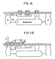
- La figure 1A représente la structure d'un transistor bipolaire NPN classique qui met en évidence la présence d'un transistor PNP parasite entre la région d'isolation et la région base.
- La figure 1 B représente la même structure mais avec une métallisation différente qui permet de réaliser un transistor FET à canal P qui constitue la structure de test.
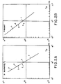
- La figure 2A représente la variation de la fonction fiabilité R en fonction du temps de défaillance Tso en heures, quand R=NSS · Neff · ND 1/2, (NSS est.la densité des charges d'interface, Neff est la charge équivalente de l'oxyde et No la concentration en atomes/cm3 de la couche épitaxiale.
- La figure 2B représente les variations de la fonction fiabilité R' en fonction du temps de défaillance T50 en heures quand R'=NSS · Neff.
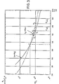
- La figure 3 représente les courbes Eox=I(ND) et ND=H(Eox) où Eox est l'épaisseur de la couche d'oxyde de passivation donnée en nanomètre.
- La figure 4 représente le bloc diagramme de calcul des paramètres prépondérants de la fonction fiabilité R dans une application informatisée.
- FIG. 1A represents the structure of a conventional NPN bipolar transistor which highlights the presence of a parasitic PNP transistor between the isolation region and the base region.
- FIG. 1B represents the same structure but with a different metallization which makes it possible to produce a P-channel FET transistor which constitutes the test structure.
- FIG. 2A represents the variation of the reliability function R as a function of the failure time T so in hours, when R = N SS · N eff · N D 1/2 , (N SS is the density of the interface charges, N eff is the equivalent charge of the oxide and N o the concentration in atoms / cm 3 of the epitaxial layer.
- FIG. 2B represents the variations of the reliability function R 'as a function of the failure time T 50 in hours when R' = N SS · N eff .
- FIG. 3 represents the curves E ox = I (N D ) and N D = H (E ox ) where E ox is the thickness of the passivation oxide layer given in nanometers.
- FIG. 4 represents the block diagram for calculating the preponderant parameters of the reliability function R in a computerized application.
Sur la figure 1A on a représente un transistor bipolaire NPN classique comportant des régions émetteur, base et collecteur, des régions de sous-collecteur et de traversée de collecteur, formées dans un caisson isolé de la couche épitaxiale par des régions d'isolation. Comme on l'a mentionné ci-dessus, le défaut en fiabilité résulte d'un courant de fuite qui s'établit dans le transistor parasite, entre les deux régions de type P. Diverses observations ont mis en évidence que ce courant de fuite avait pour cause des instabilités dans la charge de l'oxyde de passivation. Pour comprendre le phénomène d'instabilités dans les charges d'oxyde, on a procédé d'abord à une étude théorique du phénomène et à la mise en évidence de tous les paramètres intervenants dans ce phénomène d'instabilité (c'est l'objet de la partie 1), puis par une étude empirique et systématique, on a établi une corrélation entre certains de ces paramètres considérés comme prépondérants, avec le temps de défaillance T (par exemple le Tso), c'est l'objet de la partie Il qui constitue en fait le procédé de caractérisation de la présente invention. Dans la partie III de cet exposé, on donne le mode de calcul de ces paramètres prépondérants. Enfin la mise en oeuvre industrielle du procédé de caractérisation est décrite dans la partie IV.In FIG. 1A there is shown a conventional NPN bipolar transistor comprising emitter, base and collector regions, sub-collector and collector crossing regions, formed in a box isolated from the epitaxial layer by isolation regions. As mentioned above, the reliability fault results from a leakage current which is established in the parasitic transistor, between the two P-type regions. Various observations have demonstrated that this leakage current had due to instabilities in the charge of the passivation oxide. To understand the phenomenon of instabilities in oxide charges, we first carried out a theoretical study of the phenomenon and the identification of all the parameters involved in this phenomenon of instability (this is the object of part 1), then by an empirical and systematic study, we established a correlation between some of these parameters considered as preponderant, with the failure time T (for example T so ), this is the object of the part II which in fact constitutes the characterization process of the present invention. In part III of this presentation, the method for calculating these preponderant parameters is given. Finally, the industrial implementation of the characterization process is described in part IV.
Pratiquement on peut toujours trouver une structure FET telle que celle représentée sur la figure 1 B. Si ce n'était pas le cas, il suffit de modifier les masques: gravure des fenêtres dans l'oxyde et gravure du métal d'interconnexion, pour l'obtenir, et passer d'un transistor NPN bipolaire à un transistor FET à canal P.In practice, we can always find a FET structure such as that shown in FIG. 1 B. If this were not the case, it is enough to modify the masks: etching of the windows in oxide and etching of the interconnection metal, to get it, and go from a bipolar NPN transistor to a P-channel FET transistor
On utilise donc un transistor FET, dont la région source est constituée par la région d'isolation supérieure et le drain par la région base du transistor NPN; la surface de la couche épitaxiale située entre ces régions forme la région de canal. La métallisation assure que VG=VD. En tout état de cause le transistor FET représenté sur la figure 1 B, constitue la structure de test. La seule contrainte est que la tension de seuil VT du FET doit être inférieure à la tension de claquage de la jonction, pour rendre.les mesures possibles.An FET transistor is therefore used, the source region of which is constituted by the upper isolation region and the drain by the base region of the NPN transistor; the surface of the epitaxial layer located between these regions forms the channel region. The metallization ensures that V G = V D. In any event, the FET transistor shown in FIG. 1B constitutes the test structure. The only constraint is that the threshold voltage V T of the FET must be less than the breakdown voltage of the junction, to make the measurements possible.
Pour obtenir une caractérisation complète de l'oxyde, il a fallu d'abord comprendre la nature des différentes charges en présence.To obtain a complete characterization of the oxide, it was first necessary to understand the nature of the different charges present.
Le courant de fuite qui apparaît entre les deux régions P semble résulter de la présence de charges induites à la surface du silicium. C'est-à-dire qu'il peut être crée par des charges mobiles dans l'oxyde ou par une injection de porteurs à partir du silicium. Une charge négative est cependant nécessaire à l'interface Si-Si02 pour créer un chemin conducteur dans le silicium.The leakage current which appears between the two regions P seems to result from the presence of charges induced on the surface of the silicon. That is to say, it can be created by mobile charges in the oxide or by injection of carriers from silicon. A negative charge is however necessary at the Si-Si0 2 interface to create a conductive path in the silicon.
Une telle condition peut se produire quand on a des ions mobiles négatifs dans l'oxyde qui peuvent dériver vers l'interface durant l'étuvage; des ions négatifs immobiles, neutralisés par des ions mobiles positifs, qui peuvent dériver à partir de l'interface laissant en place une charge négative, une injection d'électrons du silicium vers l'oxyde et le piégeage des électrons dans l'oxyde.Such a condition can occur when there are negative mobile ions in the oxide which can drift towards the interface during baking; stationary negative ions, neutralized by positive mobile ions, which can drift from the interface leaving a negative charge in place, injecting electrons from silicon to the oxide and trapping the electrons in the oxide.
Différentes expérimentations ont mis en évidence que le phénomène d'inversion de la région N (qui crée le courant de fuite), ne résidait pas dans le déplacement des charges mobiles positives ou négatives. On a alors démontré qu'une injection d'électrons du silicium dans l'oxyde se produisait pendant l'étuvage et que ces électrons lorsqu'ils étaient piégés près de l'interface, étaient essentiellement responsables du courant de fuite.Different experiments have shown that the phenomenon of inversion of the N region (which creates the leakage current), did not reside in the displacement of the positive or negative mobile charges. It was then shown that an injection of silicon electrons into the oxide occurs during parboiling and that these electrons when trapped near the interface, are essentially responsible for the leakage current.
On a donc finalement conclu que le courant de fuite ne dépendait pas des paramètres physiques de l'oxyde (densité, qualité, etc.) mais de certains paramètres électriques Neff (densité de charges dans l'oxyde), Nss (densité d'états d'interface) et, ND (concentration de la couche épitaxiale), ci-après dénommés paramètres prépondérants qui seuls caractérisaient à la fois le courant électronique qui se produit lors de l'étuvage (composé du courant de diffusion, du courant de recombinaison à l'interface, du courant d'émission d'électrons du silicium vers l'oxyde crée par émission électronique et par effet tunnel) et le piégeage des électrons dans l'oxyde (fonction du nombre de piéges, etc.).It was therefore finally concluded that the leakage current did not depend on the physical parameters of the oxide (density, quality, etc.) but on certain electrical parameters N eff (charge density in the oxide), N ss (density d 'interface states) and, N D (concentration of the epitaxial layer), hereinafter called preponderant parameters which alone characterized both the electronic current which occurs during steaming (composed of the diffusion current, the recombination current at the interface, the electron emission current from silicon to the oxide created by electronic emission and by tunnel effect) and the trapping of electrons in the oxide (depending on the number of traps, etc.).
Aucune corrélation entre chacun de ces trois paramètres Neff, NSS et ND qui caractérisent le courant de fuite et les résultats de fiabilité n'a pu être trouvée. Après une étude systématique, effectuée en comparant les données du traitement d'étuvage et les résultats de caractérisation du FET, une très bonne corrélation a cependant pu être trouvée entre le temps de défaillance T (par exemple le T50) et le produit de la densité d'états d'interface NSS; de la densité de charges de l'oxyde Neff et la racine carrée de la concentration de la couche épitaxiale No. Pour cinq lots différents de tranches, numérotés A à E, on a mesuré tout d'abord les paramètres ND, Neff et NSS à l'aide d'un mode de calcul qui sera détaillé dans la partie III de la description et on a rassemblé les résultats dans la table ci-dessous:

Ensuite les tranches ont subi les étapes de vieillissement en étuve qui ont été détaillées ci-dessus et on a mesuré le T50 pour chacun de ces lots. On a reporté sur la figure 2A en ordonnée, le produit de la fonction fiabilité R=NSS×Neff×ND 1/2 et en abscisse les différents temps de défaillance T50. On se rend compte de l'excellente corrélation qui existe entre la fonction fiabilité et les résultats en fiabilité, qui est clairement mise en évidence par la courbe de la figure 2A.Then the slices underwent the stages of aging in an oven which were detailed above and the T 50 was measured for each of these batches. The product of the reliability function R = N SS × N eff × N D 1/2 is plotted on the ordinate on the ordinate and the different failure times T 50 on the abscissa. One realizes the excellent correlation which exists between the reliability function and the results in reliability, which is clearly highlighted by the curve of figure 2A.
La figure 2B montre une fonction fiabilité R'=NSS×Neff qui ne tient compte que du phénomène de piégeage des charges et donc ne fait pas intervenir le niveau de dopage de l'épitaxie (No); cette fonction fournit des résultats légèrement inférieurs, en particulier pour le lot C.FIG. 2B shows a reliability function R '= N SS × N eff which only takes account of the charge trapping phenomenon and therefore does not involve the doping level of the epitaxy (N o ); this function provides slightly lower results, especially for lot C.
Pour obtenir une caractérisation compléte de l'oxyde, deux séries de mesures ont été effectuées. Elles concernent les courbes ID-VG respectivement en faible inversion et en forte inversion.To obtain a complete characterization of the oxide, two series of measurements were carried out. They relate to the curves I D -V G respectively in weak inversion and in strong inversion.
On mesure le Vr du transistor FET de test montré sur la figure 1B et on le polarise à une tension légèrement inférieure (par exemple de deux volts). Les équations qui décrivent le comportement du FET, en inversion faible sont connues dans la littérature, on pourra notamment se référer à l'article: "Inadequacy of the Classical Theory of the MOS Transistor Under Weak Inversion" par R. J. Van Overstraeten et al., IEEE Trans. On Electron Devices, Vol. ED20, décembre 1973. Si on appelle η la pente de la courbe ID-VG telle que


En combinant (1) et (2) on élimine Css et on obtient:


Eox et ND seront calculés à partir des courbes ID-VG en saturation.E ox and N D will be calculated from the I D -V G curves in saturation.
On parle de capacité équivalente d'oxyde Cox et d'épaisseur équivalente d'oxyde Eox, dans le cas où la couche de passivation ne serait pas une simple couche de Si02 mais par exemple une couche composite SiO2/Si3N4SiO2.We speak of equivalent capacity of oxide C ox and equivalent thickness of oxide E ox , in the case where the passivation layer is not a simple layer of Si0 2 but for example a composite layer SiO 2 / Si 3 N 4 SiO 2 .
On polarise le FET de telle sorte qu'il soit en forte inversion, et donc en saturation. Les équations qui régissent le comportent du FET dans ces conditions peuvent être trouvées dans la référence suivante: N.A.T.O.: "Advanced Study Institute for IC Design" 19-29 juillet 1977 F. M. Klaasen-Review of Physical Models for MOS Transistor. Publié par l'Université Catholique de Louvain. La tension de seuil VT en saturation VTS est fournie par la relation:

En effectuant deux mesures de la tension de seuil VTS1 et VTS2 correspondants à deux polarisations de source différentes VS1, et VS2 déterminées, et en effectuant VTS2-VTS1 on aboutit au calcul de k soit: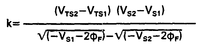
Ensuite on tire Qox de (6) sachant que Qox=qNeff d'où
Neff est une fonction de Eox (à travers Cox) et de ND (à travers k), on peut donc écrire:
Or on sait que d'après (7):

On remarque que ND est un paramètre du procédé et qu'il est en principe connu d'après la spécification. Cette mesure a seulement pour objet une détermination plus précise.It is noted that N D is a parameter of the process and that it is in principle known from the specification. This measurement is only for a more precise determination.
Le problème consiste à déterminer Eox. L'épaisseur équivalente de l'oxyde Eox est calculée à partir de la pente s2 de la courbe ID-VG en saturation, c'est-à-dire à partir de ID=s2 (VG-VT)2. On sait d'après les enseignements de la référence Klaasen que:


Expressions dans lesquelles εox est la permittivité de l'oxyde, est représente la permittivité du silicium, µP la mobilité des trous, W et L représentent respectivement la largeur et la longueur du dispositif FET (voir figure 1B).Expressions in which ε ox is the permittivity of the oxide, is represents the permittivity of silicon, µ P the mobility of the holes, W and L represent respectively the width and the length of the FET device (see Figure 1B).
Les grandeurs W et L sont déterminées à partir d'une mesure optique, et I est déterminée par le calcul.The quantities W and L are determined from an optical measurement, and I is determined by calculation.
Des équations (12), (13), et (14) on tire la valeur de Eox 

En résumé des caractéristiques ID-VG en saturation on a obtenu deux équations, l'une à partir des mesures de tension de seuil en saturation qui fournit:

La figure 3 montre dans un cas particulier réel, la forme de ces courbes, l'intersection des courbes H et 1 fournit les solutions Eox et ND (dans le cas montré sur la figure 3, on trouve Eox≠570 nm et ND≠2,21016 atomes/cm3. Les valeurs trouvées pour Eox et ND sont reportées dans l'équation (8), d'où la détermination de Neff, et dans l'équation (4) pour la détermination de NSS.Figure 3 shows in a real particular case, the shape of these curves, the intersection of curves H and 1 provides the solutions E ox and N D (in the case shown in Figure 3, we find E ox ≠ 570 nm and N D ≠ 2,210 16 atoms / cm 3. The values found for E ox and N D are reported in equation (8), hence the determination of N eff , and in equation (4) for the determination of N SS .
Le bloc diagramme du calcul des paramètres prépondérants de la fonction fiabilité R, c'est-à-dire Neff, No et Nss est montré sur la figure 4. La présence du bloc 21 signifie que toutes les données de départ qui résultent des mesures directes tant électriques (VTS1, VTS2. VS1, VS2, η, s...) qu'optiques (W, L) sont élaborées pour constituer la base de données de travail. Dans le bloc 22, on élabore les fonctions Eox=I(ND) et ND=H(Eox). Puis on cherche par itération successive à approcher les valeurs ND et Eox qui correspondent aux coordonnées du point M (figure 3). Pour cela, on utilise la valeur NDo fournie par les instructions de fabrication, qui fournit une valeur approchée de ND, en utilisant la courbe ND=H(Eox), on trouve le point MO qui fournit la valeur (Eox)o, qui à son tour fournit M1. On s'assure préalablement de la convergence des points M0, M1,..., vers le point M. C'est le rôle du bloc 23. Dans le bloc 24 le calcul des itérations successives M0, M1, M2,..., Mn es poursuivi, jusqu'à ce que la précision désirée soit atteinte (bloc 25). Les résultats, c'est-à-dire les valeurs ND, NSS, Neff et Eox sont disponibles dans le bloc 26, et la valeur de la fonction fiabilité R dans le bloc 27. Le bloc diagramme représenté sur la figure 4 peut servir de base à la mise en ceuvre d'un programme informatique.The block diagram of the calculation of the preponderant parameters of the reliability function R, that is to say N eff , N o and N ss is shown in FIG. 4. The presence of
Sur le plan industriel, le procédé de caractérisation s'implémente de la façon suivante:
- On étalonne d'abord une ligne de fabrication donnée en calculant la fonction R pour deux (ou plus) lots différents de tranches et on détermine après étuvage les temps de défaillance T50 correspondants. On trace la courbe R=f(T5o). Ensuite pour un lot déterminé il suffit de calculer sa fonction fiabilité R1 et de déduire directement de la courbe R=f(T50), son temps de défaillance (T50)1 correspondant, évitant ainsi les opérations complexes et longues d'étuvage.
- A given production line is first calibrated by calculating the R function for two (or more) different batches of wafers and the corresponding failure times T 50 are determined after baking. We draw the curve R = f (T 5o ). Then for a given batch, it is sufficient to calculate its reliability function R1 and to deduce directly from the curve R = f (T 50 ), its corresponding failure time (T 50 ) 1 , thus avoiding complex and long steaming operations.
Ce procédé présente donc un intérêt considérable à la fois pour les lignes pilotes utilisées pour faire du développement de technologie, car il fait gagner un temps précieux pour le développement d'un nouveau produit semi-conducteur, et pour les lignes de fabrication, car il permet une réaction rapide en cas d'apparition d'un défaut en fiabilité, son étude d'abord puis sa correction. Il en résulte une réduction significative de la quantité des tranches défectueuses fabriquées.This process is therefore of considerable interest both for the pilot lines used for developing technology, because it saves precious time for the development of a new semiconductor product, and for manufacturing lines, because it allows a rapid reaction in the event of a reliability defect, its study first and then its correction. This results in a significant reduction in the quantity of defective wafers produced.
Par exemple avec ce procédé de caractérisation on a pu mettre très rapidement en évidence des défauts d'auto-dopage des régions P ou encore des défauts d'alignement des régions d'isolement de type P supérieurès. On encore que l'étapè classique de recuit, 400°C, 25 minutes effectuée après la formation des conducteurs d'aluminium, en fin de procédé n'était bénéfique que si. elle était réalisée dans une atmosphère d'hydrogène. En effet, on a trouvé les résultats suivants:

Le produit standard correspondait pratiquement au lot C de la figure 2A alors que le produit après recuit en hydrogène est référence en F sur cette même figure, et présente un T50 de 2000 heures. Cette amélioration a donc été détectée immédiatement, le calcul de la fonction fiabilité s'effectuant rapidement à l'aide de la technique de calcul décrite ci-après (partie III et figure 4). Cette variante à l'étape de recuit a pu être mise en place aussitôt en ligne de fabrication.The standard product corresponded practically to batch C of FIG. 2A whereas the product after annealing in hydrogen is reference in F on this same figure, and has a T 50 of 2000 hours. This improvement was therefore detected immediately, the calculation of the reliability function being carried out quickly using the calculation technique described below (part III and FIG. 4). This variant in the annealing step could be implemented immediately on the production line.
Claims (3)
Priority Applications (4)
| Application Number | Priority Date | Filing Date | Title |
|---|---|---|---|
| EP81430036A EP0077862B1 (en) | 1981-10-28 | 1981-10-28 | Process for characterising the reliability behaviour of bipolar semiconductor devices |
| DE8181430036T DE3173901D1 (en) | 1981-10-28 | 1981-10-28 | Process for characterising the reliability behaviour of bipolar semiconductor devices |
| JP57135806A JPS5879732A (en) | 1981-10-28 | 1982-08-05 | Method of diagnosing bipolar semiconductor device |
| US06/435,139 US4520448A (en) | 1981-10-28 | 1982-10-18 | Method of characterizing reliability in bipolar semiconductor devices |
Applications Claiming Priority (1)
| Application Number | Priority Date | Filing Date | Title |
|---|---|---|---|
| EP81430036A EP0077862B1 (en) | 1981-10-28 | 1981-10-28 | Process for characterising the reliability behaviour of bipolar semiconductor devices |
Publications (2)
| Publication Number | Publication Date |
|---|---|
| EP0077862A1 EP0077862A1 (en) | 1983-05-04 |
| EP0077862B1 true EP0077862B1 (en) | 1986-02-26 |
Family
ID=8188600
Family Applications (1)
| Application Number | Title | Priority Date | Filing Date |
|---|---|---|---|
| EP81430036A Expired EP0077862B1 (en) | 1981-10-28 | 1981-10-28 | Process for characterising the reliability behaviour of bipolar semiconductor devices |
Country Status (4)
| Country | Link |
|---|---|
| US (1) | US4520448A (en) |
| EP (1) | EP0077862B1 (en) |
| JP (1) | JPS5879732A (en) |
| DE (1) | DE3173901D1 (en) |
Families Citing this family (26)
| Publication number | Priority date | Publication date | Assignee | Title |
|---|---|---|---|---|
| IT1215273B (en) * | 1985-05-09 | 1990-01-31 | Ates Componenti Elettron | PROCEDURE AND DEVICE FOR IDENTIFYING PARASITIC TRANSISTORS IN AN INTEGRATED STRUCTURE. |
| US4860080A (en) * | 1987-03-31 | 1989-08-22 | General Electric Company | Isolation for transistor devices having a pilot structure |
| US5646540A (en) * | 1989-04-19 | 1997-07-08 | Interuniversitair Micro-Elektronic Centrum Vzw | Apparatus and method for measuring electromagnetic ageing parameter of a circuit element and predicting its values |
| US5107320A (en) * | 1989-08-09 | 1992-04-21 | National Semiconductor Corporation | Method and apparatus for improvement of interconnection capacitance |
| US5262672A (en) * | 1989-08-09 | 1993-11-16 | National Semiconductor Corporation | Apparatus for improvement of interconnection capacitance |
| US5410490A (en) * | 1991-09-03 | 1995-04-25 | Hewlett-Packard Company | Electromigration verification method and apparatus |
| US5519336A (en) * | 1992-03-03 | 1996-05-21 | Honeywell Inc. | Method for electrically characterizing the insulator in SOI devices |
| US5325054A (en) * | 1992-07-07 | 1994-06-28 | Texas Instruments Incorporated | Method and system for screening reliability of semiconductor circuits |
| US5394101A (en) * | 1993-01-15 | 1995-02-28 | National Semiconductor Corporation | Method for detecting mobile ions in a semiconductor device |
| US5600578A (en) * | 1993-08-02 | 1997-02-04 | Advanced Micro Devices, Inc. | Test method for predicting hot-carrier induced leakage over time in short-channel IGFETs and products designed in accordance with test results |
| US5598102A (en) * | 1993-08-19 | 1997-01-28 | Texas Instruments Incorporated | Method for detecting defects in semiconductor insulators |
| JPH07130817A (en) * | 1993-10-30 | 1995-05-19 | Sony Corp | Metal wiring reliability evaluation method and metal wiring reliability evaluation device |
| US5486772A (en) * | 1994-06-30 | 1996-01-23 | Siliconix Incorporation | Reliability test method for semiconductor trench devices |
| US5485097A (en) * | 1994-08-08 | 1996-01-16 | Advanced Micro Devices, Inc. | Method of electrically measuring a thin oxide thickness by tunnel voltage |
| JP3206374B2 (en) * | 1995-06-19 | 2001-09-10 | 松下電器産業株式会社 | Circuit functional block reliability test method |
| DE19610065A1 (en) * | 1996-03-14 | 1997-09-18 | Siemens Ag | Method for estimating the lifetime of a power semiconductor device |
| US6275059B1 (en) | 1997-04-04 | 2001-08-14 | University Of Florida | Method for testing and diagnosing MOS transistors |
| US5986281A (en) * | 1997-10-23 | 1999-11-16 | Lucent Technologies, Inc. | Circuit and method for predicting failure rates in a semiconductor device |
| US6425111B1 (en) * | 1999-12-30 | 2002-07-23 | The Board Of Trustees Of The Leland Stanford Junior University | Saturation region transistor modeling for geometric programming |
| CN100375257C (en) * | 2003-05-23 | 2008-03-12 | 上海宏力半导体制造有限公司 | Semiconductor testing structure for clearing leakage current generating reason |
| JP4675043B2 (en) * | 2003-12-26 | 2011-04-20 | 株式会社豊田中央研究所 | Bipolar transistor, bipolar transistor characteristic variation model formula identification method, and bipolar transistor pass / fail judgment method |
| US7298159B1 (en) * | 2005-07-07 | 2007-11-20 | National Semiconductor Corporation | Method of measuring the leakage current of a deep trench isolation structure |
| US8935143B2 (en) | 2010-12-15 | 2015-01-13 | IP Cube Partners Co., Ltd. | Semiconductor sensor reliability |
| US8680523B2 (en) | 2010-12-16 | 2014-03-25 | IP Cube Partners (ICP) Co., Ltd. | Sensor for semiconductor degradation monitoring and modeling |
| RU2694169C1 (en) * | 2018-12-21 | 2019-07-09 | Федеральное государственное бюджетное образовательное учреждение высшего образования "Национальный исследовательский Мордовский государственный университет им. Н.П. Огарёва" | Method for determining limiting value of blocking voltage of power transistors |
| US11754625B2 (en) * | 2020-01-30 | 2023-09-12 | Kla Corporation | System and method for identifying latent reliability defects in semiconductor devices |
Family Cites Families (7)
| Publication number | Priority date | Publication date | Assignee | Title |
|---|---|---|---|---|
| US3335340A (en) * | 1964-02-24 | 1967-08-08 | Ibm | Combined transistor and testing structures and fabrication thereof |
| US3889188A (en) * | 1973-07-30 | 1975-06-10 | Ibm | Time zero determination of FET reliability |
| US3939381A (en) * | 1974-03-22 | 1976-02-17 | Mcm Industries, Inc. | Universal burn-in fixture |
| GB1559583A (en) * | 1975-07-18 | 1980-01-23 | Tokyo Shibaura Electric Co | Complementary mosfet device and method of manufacturing the same |
| US4180439A (en) * | 1976-03-15 | 1979-12-25 | International Business Machines Corporation | Anodic etching method for the detection of electrically active defects in silicon |
| US4144493A (en) * | 1976-06-30 | 1979-03-13 | International Business Machines Corporation | Integrated circuit test structure |
| US4281449A (en) * | 1979-12-21 | 1981-08-04 | Harris Corporation | Method for qualifying biased burn-in integrated circuits on a wafer level |
-
1981
- 1981-10-28 EP EP81430036A patent/EP0077862B1/en not_active Expired
- 1981-10-28 DE DE8181430036T patent/DE3173901D1/en not_active Expired
-
1982
- 1982-08-05 JP JP57135806A patent/JPS5879732A/en active Granted
- 1982-10-18 US US06/435,139 patent/US4520448A/en not_active Expired - Fee Related
Also Published As
| Publication number | Publication date |
|---|---|
| DE3173901D1 (en) | 1986-04-03 |
| JPS5879732A (en) | 1983-05-13 |
| US4520448A (en) | 1985-05-28 |
| JPS632141B2 (en) | 1988-01-18 |
| EP0077862A1 (en) | 1983-05-04 |
Similar Documents
| Publication | Publication Date | Title |
|---|---|---|
| EP0077862A1 (en) | Process for characterising the reliability behaviour of bipolar semiconductor devices | |
| FR2593640A1 (en) | INTEGRATED MONOLITHIC SEMICONDUCTOR DEVICE HAVING BIPOLAR JUNCTION TRANSISTORS, CMOS AND DMOS TRANSISTORS, LOW LEAKAGE DIODES, AND METHOD OF MANUFACTURING THE SAME | |
| US9627502B2 (en) | Circuit arrangement and method of forming a circuit arrangement | |
| CN101926005B (en) | Structure and method for elimination of process-related defects in poly/metal plate capacitors | |
| KR20090074206A (en) | Evaluation Method of Semiconductor Wafers | |
| JP5434491B2 (en) | Semiconductor substrate evaluation method and semiconductor device manufacturing method | |
| JP5751531B2 (en) | Semiconductor substrate evaluation method, semiconductor substrate for evaluation, semiconductor device | |
| EP0797252A2 (en) | Silicon on insulator substrate for fabricating transistors and method for preparing such a substrate | |
| JP5967019B2 (en) | Semiconductor wafer evaluation method | |
| US5841294A (en) | Method for measuring leakage current in junction region of semiconductor device | |
| EP3772093A1 (en) | Manufacturing method comprising definition of an effective length of mosfet transistor channel | |
| US7335518B2 (en) | Method for manufacturing semiconductor device | |
| Jerome et al. | The effect of trench processing conditions on complementary bipolar analog devices with SOI/Trench isolation | |
| FR3066025A1 (en) | METHOD OF ELECTRICAL CHARACTERIZATION OF MOS TRANSISTOR ON SELF | |
| US7351595B2 (en) | Method for manufacturing semiconductor device | |
| JP3163756B2 (en) | Semiconductor device and method of manufacturing semiconductor device | |
| CN100399498C (en) | Manufacturing method of semiconductor device | |
| FR3057104A1 (en) | FIELD EFFECT TRANSISTORS OF FDSOI TYPE | |
| JPH10270517A (en) | Method for measuring carrier concentration of p-type silicon epitaxial layer | |
| FR2667726A1 (en) | SEMICONDUCTOR DEVICE HAVING DOUBLE DOPED CHANNEL STOP LAYER AND METHOD FOR MANUFACTURING THE SAME | |
| CN119178976A (en) | Method, system, device and storage medium for obtaining threshold voltage stability | |
| JP2005150208A (en) | Evaluation method of soi wafer | |
| CN119069348A (en) | Method for manufacturing insulated gate bipolar transistor | |
| EP0081422B1 (en) | Integrated process for manufacturing logical circuits comprising at least one field effect transistor having a low threshold voltage and a saturation resistor, and logical circuit made by that process | |
| JPH0691145B2 (en) | Semiconductor wafer sorting method |
Legal Events
| Date | Code | Title | Description |
|---|---|---|---|
| PUAI | Public reference made under article 153(3) epc to a published international application that has entered the european phase |
Free format text: ORIGINAL CODE: 0009012 |
|
| 17P | Request for examination filed |
Effective date: 19811125 |
|
| AK | Designated contracting states |
Designated state(s): DE FR GB |
|
| GRAA | (expected) grant |
Free format text: ORIGINAL CODE: 0009210 |
|
| AK | Designated contracting states |
Designated state(s): DE FR GB |
|
| REF | Corresponds to: |
Ref document number: 3173901 Country of ref document: DE Date of ref document: 19860403 |
|
| PLBE | No opposition filed within time limit |
Free format text: ORIGINAL CODE: 0009261 |
|
| STAA | Information on the status of an ep patent application or granted ep patent |
Free format text: STATUS: NO OPPOSITION FILED WITHIN TIME LIMIT |
|
| 26N | No opposition filed | ||
| PGFP | Annual fee paid to national office [announced via postgrant information from national office to epo] |
Ref country code: DE Payment date: 19911102 Year of fee payment: 11 |
|
| PGFP | Annual fee paid to national office [announced via postgrant information from national office to epo] |
Ref country code: FR Payment date: 19920928 Year of fee payment: 12 |
|
| PG25 | Lapsed in a contracting state [announced via postgrant information from national office to epo] |
Ref country code: DE Effective date: 19930701 |
|
| PGFP | Annual fee paid to national office [announced via postgrant information from national office to epo] |
Ref country code: GB Payment date: 19930922 Year of fee payment: 13 |
|
| PG25 | Lapsed in a contracting state [announced via postgrant information from national office to epo] |
Ref country code: FR Effective date: 19940630 |
|
| REG | Reference to a national code |
Ref country code: FR Ref legal event code: ST |
|
| PG25 | Lapsed in a contracting state [announced via postgrant information from national office to epo] |
Ref country code: GB Effective date: 19941028 |
|
| GBPC | Gb: european patent ceased through non-payment of renewal fee |
Effective date: 19941028 |