EP0078492A2 - Procédé pour commander un dispositif de mémoire - Google Patents
Procédé pour commander un dispositif de mémoire Download PDFInfo
- Publication number
- EP0078492A2 EP0078492A2 EP82109893A EP82109893A EP0078492A2 EP 0078492 A2 EP0078492 A2 EP 0078492A2 EP 82109893 A EP82109893 A EP 82109893A EP 82109893 A EP82109893 A EP 82109893A EP 0078492 A2 EP0078492 A2 EP 0078492A2
- Authority
- EP
- European Patent Office
- Prior art keywords
- blocks
- data
- alternative
- recording
- defective
- Prior art date
- Legal status (The legal status is an assumption and is not a legal conclusion. Google has not performed a legal analysis and makes no representation as to the accuracy of the status listed.)
- Granted
Links
- 238000000034 method Methods 0.000 title claims abstract description 60
- 230000002950 deficient Effects 0.000 claims abstract description 75
- 230000004044 response Effects 0.000 claims description 5
- 230000015654 memory Effects 0.000 description 13
- 230000003287 optical effect Effects 0.000 description 7
- 238000011084 recovery Methods 0.000 description 5
- 230000005856 abnormality Effects 0.000 description 3
- 238000010586 diagram Methods 0.000 description 2
- 230000000694 effects Effects 0.000 description 2
- 230000002159 abnormal effect Effects 0.000 description 1
- 230000003111 delayed effect Effects 0.000 description 1
- 230000008030 elimination Effects 0.000 description 1
- 238000003379 elimination reaction Methods 0.000 description 1
Images


Classifications
-
- G—PHYSICS
- G11—INFORMATION STORAGE
- G11B—INFORMATION STORAGE BASED ON RELATIVE MOVEMENT BETWEEN RECORD CARRIER AND TRANSDUCER
- G11B20/00—Signal processing not specific to the method of recording or reproducing; Circuits therefor
- G11B20/10—Digital recording or reproducing
- G11B20/18—Error detection or correction; Testing, e.g. of drop-outs
- G11B20/1883—Methods for assignment of alternate areas for defective areas
-
- G—PHYSICS
- G11—INFORMATION STORAGE
- G11B—INFORMATION STORAGE BASED ON RELATIVE MOVEMENT BETWEEN RECORD CARRIER AND TRANSDUCER
- G11B20/00—Signal processing not specific to the method of recording or reproducing; Circuits therefor
- G11B20/10—Digital recording or reproducing
- G11B20/18—Error detection or correction; Testing, e.g. of drop-outs
- G11B20/1833—Error detection or correction; Testing, e.g. of drop-outs by adding special lists or symbols to the coded information
-
- G—PHYSICS
- G11—INFORMATION STORAGE
- G11B—INFORMATION STORAGE BASED ON RELATIVE MOVEMENT BETWEEN RECORD CARRIER AND TRANSDUCER
- G11B7/00—Recording or reproducing by optical means, e.g. recording using a thermal beam of optical radiation by modifying optical properties or the physical structure, reproducing using an optical beam at lower power by sensing optical properties; Record carriers therefor
- G11B7/007—Arrangement of the information on the record carrier, e.g. form of tracks, actual track shape, e.g. wobbled, or cross-section, e.g. v-shaped; Sequential information structures, e.g. sectoring or header formats within a track
-
- G—PHYSICS
- G11—INFORMATION STORAGE
- G11B—INFORMATION STORAGE BASED ON RELATIVE MOVEMENT BETWEEN RECORD CARRIER AND TRANSDUCER
- G11B7/00—Recording or reproducing by optical means, e.g. recording using a thermal beam of optical radiation by modifying optical properties or the physical structure, reproducing using an optical beam at lower power by sensing optical properties; Record carriers therefor
- G11B7/007—Arrangement of the information on the record carrier, e.g. form of tracks, actual track shape, e.g. wobbled, or cross-section, e.g. v-shaped; Sequential information structures, e.g. sectoring or header formats within a track
- G11B7/00736—Auxiliary data, e.g. lead-in, lead-out, Power Calibration Area [PCA], Burst Cutting Area [BCA], control information
-
- G—PHYSICS
- G11—INFORMATION STORAGE
- G11B—INFORMATION STORAGE BASED ON RELATIVE MOVEMENT BETWEEN RECORD CARRIER AND TRANSDUCER
- G11B2220/00—Record carriers by type
- G11B2220/20—Disc-shaped record carriers
-
- G—PHYSICS
- G11—INFORMATION STORAGE
- G11B—INFORMATION STORAGE BASED ON RELATIVE MOVEMENT BETWEEN RECORD CARRIER AND TRANSDUCER
- G11B7/00—Recording or reproducing by optical means, e.g. recording using a thermal beam of optical radiation by modifying optical properties or the physical structure, reproducing using an optical beam at lower power by sensing optical properties; Record carriers therefor
- G11B7/007—Arrangement of the information on the record carrier, e.g. form of tracks, actual track shape, e.g. wobbled, or cross-section, e.g. v-shaped; Sequential information structures, e.g. sectoring or header formats within a track
- G11B7/013—Arrangement of the information on the record carrier, e.g. form of tracks, actual track shape, e.g. wobbled, or cross-section, e.g. v-shaped; Sequential information structures, e.g. sectoring or header formats within a track for discrete information, i.e. where each information unit is stored in a distinct discrete location, e.g. digital information formats within a data block or sector
Definitions
- the present invention relates to a method of controlling a storage device and, more particularly, to a method of assigning an alternative block to a data block which has caused a write error, the method being particularly suitable for use in a storage device, such as a photo disk unit, of the type where data once recorded on the recording medium can no longer be erased.
- Photo disk units are entering into practical application as an economical mass storage device for storing immense data such as picture information.
- the photo disk is a rotary disk with a metallic film to be exposed to the laser beam deposited thereon.
- the laser beam is modulated in accordance with the information so as to form "pits" selectively on the metallic film, and when information is retrieved, a weak laser beam is projected concentrically onto the metallic film so that recorded information is picked up by sensing the variation of the reflected beam intensity which depends on the presence or absence of a pit.
- the immediate problem of the photo disk unit is how to overcome the disability of rewriting data in order to recover the error in data.
- the timing of writing is delayed and the location of the alternative block is recorded within the defective block by use of a means for avoiding a bad spot.
- a means for avoiding a bad spot For example, in a fixed-segment magnetic disk, when a defective block is detected by the check following the data writing operation, an alternative block is seeked on the alternative track so as to write data and at the same time the location of the alternative block is recorded in the defective block.
- Another method is that the recording medium is tested in advance for writing and reading, and when a defective block is accessed, it is switched to an alternative block by the hardware logics. The latter method has been practiced, for example, in magnetic drum . storage units, magnetic bubble memory units and IC memories.
- Another object of the present invention is to provide a method of controlling a recording device which achieves error recovery for defective blocks by efficient use of the recording area.
- information sets of the first group which have been written on the recording medium are read out and if a defective block is detected, data corresponding to the defective block is combined with the second pointer information which indicates the unique address of the defective block so as to produce information sets of the second group depending on the number of detected defective blocks, and the information sets of the second group are written sequentially into unused recording blocks within the alternative area starting from an alternative block corresponding to the first pointer information.
- the alternative area for the defective block can be accessed in accordance with the first pointer in the information set of the normal block adjacent to the defective block.
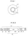
- a recording area 10 of the photo disk is divided into a normal recording area 11 which is first accessed in the reading or writing operation and an alternative area 13, as shown in Fig. 1. Both areas have a plurality of tracks, and each track is divided into a plurality of blocks (i.e., sectors) having individual sector addresses.
- the size of the alternative area 13 may be determined arbitrarily depending on the error rate of the disk, though in general far less storage capacity is assigned to the alternative area 13 than that to the normal recording area 11.
- a defective sector 12 shown by mark "x" the data to be written in this defective sector is recorded in a sector 14 which is selected out of sectors in the alternative area 13.
- alternative sectors in the alternative area 13 are used sequentially, and on this account the disk controller maintains address information indicating the sector located next to the alternative sector which has been used last, i.e., the top sector in the unused alternative area.
- the sector address can be controlled by, for example, initializing the sector address register each time the system is turned on or the photo disk is replaced so that the sector replacement process in the reading operation will start at the first sector in the alternative area 13.
- Fig. 2 shows the format of unit sector constituting the recording area 11 and alternative area 13.
- Each sector includes a sector address field 21, a gap field 22 preceding a data field, a data field 23, an error correction code (ECC) field 24, and a gap field 25 following a data field.
- the data field 23 is made up of a pointer section 23a and a pure data section 23b. For sectors in the recording area 11, the pointer section 23a is used as the pointer to an alternative sector, and for sectors in the alternative area 13, the pointer section 23a is used as the pointer to a corresponding defective sector in the recording area 11.
- the disk controller when a higher level device, e.g., a CPU channel, issues a write command for a sector or sectors of data, the disk controller provides for the pointer section 23a of the sector (s-) the pointer information indicating the common alternative sector address, then operates on a lower level device, e.g., an optical storage controller, to write the data sequentially from the specified sector position in the recording area 11 on the photo disk.
- a higher level device e.g., a CPU channel
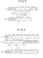
- Fig. 3 explains the foregoing control method, where reference number 11T denotes part of a track in the recording area 11, including sectors n through n+4, and 13T denotes part of a track in the alternative area 13, including sectors N through N+3.
- This example shows that sectors up to sector n on track 11T have been used and sectors up to sector N on alternative track 13T have been used.
- address data indicating the same alternative sector N+1, as shown by the arrows 30, is written in the pointer field section 23a of the sectors n+1 through n+4.
- sector n+4 causes a read error
- the preceding sector n+3 which has been read normally gives in its pointer section 23a the address N+1 of the alternative sector for these blocks.
- the alternative track 13T is seeked to read out a few sectors following the address N+1, and data in the alternative sector corresponding to the. defective sector n+4 can readily be obtained by checking the pointer section of the read-out sectors.
- FIG. 4 Another example of the occurrence of defective sector will be described with reference to Fig. 4.
- This example shows the occurrence of errors in a number of sectors within the recording area when a large amount of additional data are written.
- An assumption is made that when 24 sectors of data are additionally written in sectors n+1 through n+24 on track 11T in the data area, errors occur in three sectors n+1, n+6 and n+22.
- the disk controller assigns alternative sectors N+1, N+2 and N+3 on alternative track 13T to these defective sectors as shown by the arrows 32, 33 and 34, respectively.
- the pointer section of the sectors n+1 through n+22 on track 11T is written the address indicating sector N+l, and therefore, the pointer address contained in the preceding or following normal sector does not coincide with respective alternative sector of these defective sectors.
- the alternative track 13T is read sequentially from the address N+l indicated by the normal sector to check the pointer section 23a of each sector, it does not take much time to read alternative sectors N+2 and N+3 corresponding to the defective sectors n+6 and n+22.
- Fig. 5 shows in block diagram the arrangement of the photo disk system which employs the foregoing inventive control method.
- the arrangement includes a CPU 50, a channel 51, an optical disk controller (ODC) 60, an optical storage controller (OCS) 70, and an optical disk unit (ODU) 80.
- ODC optical disk controller
- OCS optical storage controller
- ODU optical disk unit
- the ODC 60 stores the address of the alternative sector to be used next and controls the OSC 70 in response to the write command and read command issued by the channel 51.
- the ODC 60 includes a channel interface controller 61 which is connected with the channel 51 through a data bus 102 and control lines 101, a buffer memory 62 for holding reception data temporarily, a device interface controller 63 which is connected with the OSC 70 through a data bus 103 and control lines 104, a microprocessor 64 which controls the above-mentioned components, and a memory 65 which stores the program to be executed by the microprocessor 64.
- the OSC 70 operates the ODU 80 in response to the commands from the ODC 60, and includes an ODC interface controller 71 which is connected with the data bus 103 and control lines 104, a buffer memory 72 for holding temporarily data which will be written to or has been read out from the recording area 11 of the disk, an error recovery procedure (ERP) buffer 73 for holding data which has been read out from the alternative area 13 of the disk, an ECC circuit 74, a modem circuit 75 which modulates digital data into analog signal and demodulates analog signal into digital data, an ODU interface controller 76 connected with the ODU 80, a microprocessor 77 which controls the above-mentioned components, and a memory 78 which stores the program to be executed by the microprocessor 77.
- ODC interface controller 71 which is connected with the data bus 103 and control lines 104
- a buffer memory 72 for holding temporarily data which will be written to or has been read out from the recording area 11 of the disk
- EPP error recovery procedure
- ECC circuit 74 for holding data which has
- the ODU 80 drives the photo disk and the optical read/write head under control of the OSC 70.
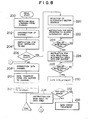
- the flowchart shown in Figs. 6 and 7 indicates the control procedures for the data writing process.
- the interface controller 61 receives the data write command issued by the channel 51 to the ODC (in routine 100)
- the microprocessor 64 transfers data of each sector sent from the channel 51 to the buffer memory 72 in the OSC (in routine 102), while appending the common sector pointer (see 23a in Fig. 2) to the data by utilization of the buffer memory 62, and suspends the connection with the channel 51 when the data transfer completes (in routine 104).
- the microprocessor 64 issues instruction to the OSC 70 in order to write data which is held in the buffer memory 72 onto the photo disk starting from the address which has been designated by the CPU separately in advance of the data write command, and thereafter issues the write & read check command (in routine 106).
- the microprocessor 64 waits for the operation completion signal of the above-mentioned command from the OSC 70 (in routine 108). During the execution of the above-mentioned command, if the write operation cannot take place due to abnormality in the ODU 80 or the power system, the OSC 70 issues status information indicating a write error together with the operation end signal. In case the write operation has been carried out successfully, if a write error which cannot be corrected by the ECC occurs, the OSC 70 also issues status information indicating this affair. Upon receipt of the operation end signal, the microprocessor 64 analyzes the status information from the OSC 70, and makes the abnormal termination in routine 112 if a write error is detected (in routine 110). If a read error is detected (in routine 114), the error recovery procedure (E R P) routines 130-140 are executed so as to transfer data in the defective sector to the alternative sector.
- E R P error recovery procedure
- routine 130 the seek command is issued to the OSC 70 in order to move the photo disk head located currently in the recording area 11 to the track position indicated by the alternative sector pointer stored in the ODC.
- the microprocessor 64 waits for the report from the OSC 70 on the completion of the seek operation (in routine 132). On receiving the report, the microprocessor 64 judges whether the current process is the first ERP for the write command from the channel (in routine 134), and if this is ture (yes), the microprocessor executes routine 136 so that the contents of the pointer field section 23a (this currently indicates one of alternative sectors) of each sector data corresponding to the defective sector stored in the buffer memory 72 are changed so as to indicate the defective sector, then the process proceeds to routine 138. If the current process is the second or later ERP, the routine 136 will be skipped.
- routine 138 the microprocessor 64 issues command to the OSC 70 so that data of the defective sector stored in the buffer 72, which has been modified in routine 136, is written in the alternative area 13, then the OSC 70 is directed to carry out the read out check.
- the microprocessor 64 modifies the contents of its alternative sector pointer in accordance with the number of alternative sectors used in the current ERP (i.e., the number of defective sectors which have occurred) (in routine 140), then the process proceeds to routine 108 and waits for the operation completion signal from the OSC.
- the process proceeds to the determination routine 116 shown in Fig. 7. If the ERP has not taken place, the process proceeds to routine 122 so as to report the completion of the write operation to the channel 51, and the program completes. If the ERP has taken place, the seek command is given to the OSC 70 in routine 118 in order to return the photo disk head located currently in the alternative area 13 to the original track position in the recording area 11..Then the microprocessor 64 waits for the report from the OSC on the completion of the seek operation (in routine 120), then proceeds to termination routine 122.
- the microprocessor 64 receives the data read command following the commands indicating the address and data length from the channel 51 through the interface 61, (in routine 200), it once suspends the connection with the channel (in routine 202), and issues a command to the OSC 70 so that the OSC stores readout data into the OSC buffer 72 (in routine 204).
- the OSC 70 operates the ODU 80, and issues a report to the ODC 60 when the read operation has completed.
- routine 208 If the data have been read normally, the ODC 60 connects with the channel (in routine 208), reads out data in the OSC buffer 72, then transfers the data, with information in the pointer section unnecessary for the CPU being removed, to the channel 51 sequentially (in routine 210). After all data have been transferred, the end signal is issued (in routine 212), and the program completes. If error is detected in data read out by the ODU 80, routines 220 through 234 are executed in order to read data in the alternative sector. First, in routine 220, the OSC buffer 72 is referenced to know the alternative sector address from the pointer contents provided by the sector which has been read normally. The OSC 70 is given the seek command basing on the address for moving the photo disk head to the alternative area (in routine 222).
- the ODC directs the OSC 70 to read a plurality of sectors of data, which is much more than the number of defective sectors occurring in the OSC buffer area 72, into the ERP buffer 73 starting from the alternative sector position which has been made known in routine 220 (in routine 226).
- the OSC 70 reports the end of operation (in routine 228) for the above read command, the pointer is checked for alternative sector data which have been read normally in the ERP buffer 73, and data corresponding to the defective sector in the buffer memory 72 is transferred from the ERP buffer 73 to the buffer memory 72 (in routine 230).
- routine 232 it is judged whether alternative sector data for all defective sectors in the buffer memory 72 have been replaced by the correct data in the E R P buffer 73, and if this is ture, the process proceeds to routine 234 to issue the command for returning the optical disk head to the data area, then the process proceeds to routine 208. If a defective sector disabling data relocation has been detected in routine 232, that means abnormality in the alternative area on the photo disk, the abnormality processing routine 236 will be executed.
- the data format of Fig. 9 is to write the address of a specific alternative sector corresponding to a defective sector into the pointer section 23a of the defective sector within the recording area 11.
- the ECC 24 corresponding to the data section 23b is appended during the first writing operation, and the alternative sector address is written in the pointer section 23a during the second wriring operation following the determination of the defective sector as a result of the data check. Therefore, in order to make the pointer contents reliable, the pointer section 23a needs to be appended with the specific ECC 23c, and it is also necessary to provide a gap 23d between the ECC 23c and the data 23b.
- the pointer section 23a and data section 23b can be written concurrently, it is sufficient to provide a common ECC field 24, and the area used for the ECC 23c and gap 23d in Fig. 9 can be saved.
- the recording medium can have a larger storage capacity.
- the following is the second example of the control method without application of the present invention, wherein the pointer to the alternative sector is not provided at all, and the entire alternative sector area which has been determined in advance is searched.
- search time for the alternative sector is not negligible, and overhead for a recording medium with a high error rate will become a large problem.
- elimination of the pointer section in each sector provides a larger effective storage capacity for the recording medium as compared with the method of the present invention, the processing ability is disadvantageously low due to the overhead.
- the location of the alternative block is recorded in the normal blocks located before and after the defective block, and error recovery for a defective sector can be achieved efficiently for a storage device using a non- rewritable recording medium, such as a photo disk, with a high error rate.
- the sector of the photo disk has been described as a data block, it will be appreciated that the inventive control method can also be applied to the recording system where the track of data is processed as a block.
Landscapes
- Engineering & Computer Science (AREA)
- Signal Processing (AREA)
- Signal Processing For Digital Recording And Reproducing (AREA)
- Techniques For Improving Reliability Of Storages (AREA)
- Optical Recording Or Reproduction (AREA)
Applications Claiming Priority (2)
| Application Number | Priority Date | Filing Date | Title |
|---|---|---|---|
| JP56173860A JPS5877034A (ja) | 1981-10-30 | 1981-10-30 | 記録方法 |
| JP173860/81 | 1981-10-30 |
Publications (3)
| Publication Number | Publication Date |
|---|---|
| EP0078492A2 true EP0078492A2 (fr) | 1983-05-11 |
| EP0078492A3 EP0078492A3 (en) | 1983-07-27 |
| EP0078492B1 EP0078492B1 (fr) | 1988-06-15 |
Family
ID=15968477
Family Applications (1)
| Application Number | Title | Priority Date | Filing Date |
|---|---|---|---|
| EP82109893A Expired EP0078492B1 (fr) | 1981-10-30 | 1982-10-26 | Procédé pour commander un dispositif de mémoire |
Country Status (4)
| Country | Link |
|---|---|
| US (1) | US4525839A (fr) |
| EP (1) | EP0078492B1 (fr) |
| JP (1) | JPS5877034A (fr) |
| DE (1) | DE3278680D1 (fr) |
Cited By (5)
| Publication number | Priority date | Publication date | Assignee | Title |
|---|---|---|---|---|
| GB2157035A (en) * | 1984-03-19 | 1985-10-16 | Olympus Optical Co | Information retrieval system |
| EP0090040A4 (fr) * | 1981-10-05 | 1986-01-28 | Digital Equipment Corp | Format de disque pour un systeme de stockage secondaire. |
| EP0127311A3 (en) * | 1983-05-23 | 1986-12-30 | Data General Corporation | Method of and controller for handling medium defects in a disc drive system |
| EP0221763A3 (en) * | 1985-11-01 | 1989-02-08 | Cipher Data Products, Inc. | System for transferring digital data between a host device and a recording medium |
| EP0282036B1 (fr) * | 1987-03-10 | 1993-09-15 | Kabushiki Kaisha Toshiba | Appareil pour enregistrer des données dans un milieu d'enregistrement optique |
Families Citing this family (75)
| Publication number | Priority date | Publication date | Assignee | Title |
|---|---|---|---|---|
| US4750107A (en) * | 1985-01-07 | 1988-06-07 | Unisys Corporation | Printer-tape data link processor with DMA slave controller which automatically switches between dual output control data chomels |
| US5202979A (en) * | 1985-05-08 | 1993-04-13 | Thinking Machines Corporation | Storage system using multiple independently mechanically-driven storage units |
| JP2516906B2 (ja) * | 1985-09-20 | 1996-07-24 | カシオ計算機株式会社 | デ−タ伝送装置 |
| US5072368A (en) * | 1985-10-31 | 1991-12-10 | International Business Machines Corporation | Immediate duplication of I/O requests on a record by record basis by a computer operating system |
| JPS6364678A (ja) * | 1986-09-05 | 1988-03-23 | Mitsubishi Electric Corp | デイスクのライトエラ−リカバリ方式 |
| US4972316A (en) * | 1987-03-30 | 1990-11-20 | International Business Machines Corporation | Method of handling disk sector errors in DASD cache |
| EP0371034A4 (en) * | 1987-07-02 | 1993-02-24 | Exabyte Corporation | Method and apparatus for data buffer management |
| US4833679A (en) * | 1987-08-31 | 1989-05-23 | International Business Machines Corporation | Method and apparatus with improved error correction and error information availability |
| US5268870A (en) * | 1988-06-08 | 1993-12-07 | Eliyahou Harari | Flash EEPROM system and intelligent programming and erasing methods therefor |
| US5268319A (en) | 1988-06-08 | 1993-12-07 | Eliyahou Harari | Highly compact EPROM and flash EEPROM devices |
| JP2852935B2 (ja) * | 1989-03-28 | 1999-02-03 | キヤノン株式会社 | 情報再生装置 |
| US5535328A (en) * | 1989-04-13 | 1996-07-09 | Sandisk Corporation | Non-volatile memory system card with flash erasable sectors of EEprom cells including a mechanism for substituting defective cells |
| US7190617B1 (en) | 1989-04-13 | 2007-03-13 | Sandisk Corporation | Flash EEprom system |
| US7447069B1 (en) | 1989-04-13 | 2008-11-04 | Sandisk Corporation | Flash EEprom system |
| EP1031992B1 (fr) | 1989-04-13 | 2006-06-21 | SanDisk Corporation | Système EEprom avec effacement en bloc |
| JP3479981B2 (ja) * | 1990-12-11 | 2003-12-15 | ブラザー工業株式会社 | 文書処理装置 |
| US5313471A (en) * | 1991-02-26 | 1994-05-17 | Matsushita Electric Industrial Co., Ltd. | Error concealing method |
| US5623507A (en) * | 1991-09-13 | 1997-04-22 | Storage Technology Corporation | Error pointers for enhanced error correction |
| EP0549152A3 (en) * | 1991-12-24 | 1993-12-08 | Advanced Micro Devices Inc | Single chip controller for optical data disk drives |
| US5493676A (en) * | 1993-06-29 | 1996-02-20 | Unisys Corporation | Severe environment data recording system |
| US5564011A (en) * | 1993-10-05 | 1996-10-08 | International Business Machines Corporation | System and method for maintaining file data access in case of dynamic critical sector failure |
| US5845313A (en) * | 1995-07-31 | 1998-12-01 | Lexar | Direct logical block addressing flash memory mass storage architecture |
| US5930815A (en) * | 1995-07-31 | 1999-07-27 | Lexar Media, Inc. | Moving sequential sectors within a block of information in a flash memory mass storage architecture |
| US8171203B2 (en) | 1995-07-31 | 2012-05-01 | Micron Technology, Inc. | Faster write operations to nonvolatile memory using FSInfo sector manipulation |
| US6801979B1 (en) | 1995-07-31 | 2004-10-05 | Lexar Media, Inc. | Method and apparatus for memory control circuit |
| US5907856A (en) * | 1995-07-31 | 1999-05-25 | Lexar Media, Inc. | Moving sectors within a block of information in a flash memory mass storage architecture |
| US6757800B1 (en) | 1995-07-31 | 2004-06-29 | Lexar Media, Inc. | Increasing the memory performance of flash memory devices by writing sectors simultaneously to multiple flash memory devices |
| US6978342B1 (en) | 1995-07-31 | 2005-12-20 | Lexar Media, Inc. | Moving sectors within a block of information in a flash memory mass storage architecture |
| US6081878A (en) | 1997-03-31 | 2000-06-27 | Lexar Media, Inc. | Increasing the memory performance of flash memory devices by writing sectors simultaneously to multiple flash memory devices |
| US5838614A (en) | 1995-07-31 | 1998-11-17 | Lexar Microsystems, Inc. | Identification and verification of a sector within a block of mass storage flash memory |
| US6728851B1 (en) * | 1995-07-31 | 2004-04-27 | Lexar Media, Inc. | Increasing the memory performance of flash memory devices by writing sectors simultaneously to multiple flash memory devices |
| US6125435A (en) * | 1995-09-13 | 2000-09-26 | Lexar Media, Inc. | Alignment of cluster address to block addresses within a semiconductor non-volatile mass storage memory |
| US5689635A (en) * | 1995-12-27 | 1997-11-18 | Sgs-Thomson Microelectronics, Inc. | Microprocessor memory test circuit and method |
| US5928370A (en) * | 1997-02-05 | 1999-07-27 | Lexar Media, Inc. | Method and apparatus for verifying erasure of memory blocks within a non-volatile memory structure |
| US6411546B1 (en) | 1997-03-31 | 2002-06-25 | Lexar Media, Inc. | Nonvolatile memory using flexible erasing methods and method and system for using same |
| US6122195A (en) * | 1997-03-31 | 2000-09-19 | Lexar Media, Inc. | Method and apparatus for decreasing block write operation times performed on nonvolatile memory |
| US6034897A (en) * | 1999-04-01 | 2000-03-07 | Lexar Media, Inc. | Space management for managing high capacity nonvolatile memory |
| JPH10312650A (ja) * | 1997-05-14 | 1998-11-24 | Ricoh Co Ltd | 光ディスク記録装置 |
| US6076137A (en) * | 1997-12-11 | 2000-06-13 | Lexar Media, Inc. | Method and apparatus for storing location identification information within non-volatile memory devices |
| GB9801373D0 (en) | 1998-01-22 | 1998-03-18 | Memory Corp Plc | Memory system |
| KR100433606B1 (ko) * | 1998-10-22 | 2004-05-31 | 마쯔시다덴기산교 가부시키가이샤 | 정보 기록 매체, 및 이의 결함을 관리하는 방법 및 장치 |
| JP2000149435A (ja) * | 1998-11-12 | 2000-05-30 | Nec Corp | 磁気ディスク装置及びこれを用いた映像記録再生装置 |
| US6374337B1 (en) | 1998-11-17 | 2002-04-16 | Lexar Media, Inc. | Data pipelining method and apparatus for memory control circuit |
| US6426928B1 (en) | 1999-03-31 | 2002-07-30 | International Business Machines Corporation | Ability to distinguish true disk write errors |
| US6247152B1 (en) | 1999-03-31 | 2001-06-12 | International Business Machines Corporation | Relocating unreliable disk sectors when encountering disk drive read errors with notification to user when data is bad |
| US6332204B1 (en) | 1999-03-31 | 2001-12-18 | International Business Machines Corporation | Recovering and relocating unreliable disk sectors when encountering disk drive read errors |
| US6141249A (en) * | 1999-04-01 | 2000-10-31 | Lexar Media, Inc. | Organization of blocks within a nonvolatile memory unit to effectively decrease sector write operation time |
| DE60030876T2 (de) | 1999-04-01 | 2007-05-03 | Lexar Media, Inc., Fremont | Bereichsverwaltung eines nichtflüchtigen Speichers mit hoher Kapazität |
| US7102671B1 (en) | 2000-02-08 | 2006-09-05 | Lexar Media, Inc. | Enhanced compact flash memory card |
| US6426893B1 (en) | 2000-02-17 | 2002-07-30 | Sandisk Corporation | Flash eeprom system with simultaneous multiple data sector programming and storage of physical block characteristics in other designated blocks |
| US6721843B1 (en) | 2000-07-07 | 2004-04-13 | Lexar Media, Inc. | Flash memory architecture implementing simultaneously programmable multiple flash memory banks that are host compatible |
| US6973014B1 (en) * | 2000-07-11 | 2005-12-06 | Sonic Solutions | Methods for optical disc sector verification |
| US7167944B1 (en) | 2000-07-21 | 2007-01-23 | Lexar Media, Inc. | Block management for mass storage |
| US6567307B1 (en) | 2000-07-21 | 2003-05-20 | Lexar Media, Inc. | Block management for mass storage |
| JP3674531B2 (ja) * | 2001-04-12 | 2005-07-20 | 株式会社日立製作所 | ファイル管理方法、ファイル管理装置、プログラム |
| KR20030023762A (ko) * | 2001-06-21 | 2003-03-19 | 코닌클리즈케 필립스 일렉트로닉스 엔.브이. | 에러 보정 방법 및 에러 보정 회로 장치 |
| GB0123416D0 (en) * | 2001-09-28 | 2001-11-21 | Memquest Ltd | Non-volatile memory control |
| GB0123421D0 (en) * | 2001-09-28 | 2001-11-21 | Memquest Ltd | Power management system |
| GB0123419D0 (en) | 2001-09-28 | 2001-11-21 | Memquest Ltd | Data handling system |
| GB0123415D0 (en) | 2001-09-28 | 2001-11-21 | Memquest Ltd | Method of writing data to non-volatile memory |
| GB0123412D0 (en) | 2001-09-28 | 2001-11-21 | Memquest Ltd | Memory system sectors |
| GB0123417D0 (en) | 2001-09-28 | 2001-11-21 | Memquest Ltd | Improved data processing |
| GB0123410D0 (en) | 2001-09-28 | 2001-11-21 | Memquest Ltd | Memory system for data storage and retrieval |
| US6957295B1 (en) | 2002-01-18 | 2005-10-18 | Lexar Media, Inc. | File management of one-time-programmable nonvolatile memory devices |
| US6950918B1 (en) | 2002-01-18 | 2005-09-27 | Lexar Media, Inc. | File management of one-time-programmable nonvolatile memory devices |
| US7231643B1 (en) | 2002-02-22 | 2007-06-12 | Lexar Media, Inc. | Image rescue system including direct communication between an application program and a device driver |
| JP4026517B2 (ja) | 2003-03-12 | 2007-12-26 | ソニー株式会社 | 記録媒体、記録装置、記録方法 |
| EP1695304A4 (fr) | 2003-12-17 | 2011-09-28 | Lexar Media Inc | Activation au point de vente d'un materiel electronique en vue d'eviter un vol |
| US7725628B1 (en) | 2004-04-20 | 2010-05-25 | Lexar Media, Inc. | Direct secondary device interface by a host |
| US7370166B1 (en) | 2004-04-30 | 2008-05-06 | Lexar Media, Inc. | Secure portable storage device |
| US7940613B2 (en) * | 2004-06-15 | 2011-05-10 | Panasonic Corporation | Drive device |
| CN101853684B (zh) * | 2004-06-15 | 2012-06-27 | 松下电器产业株式会社 | 驱动装置 |
| US7464306B1 (en) | 2004-08-27 | 2008-12-09 | Lexar Media, Inc. | Status of overall health of nonvolatile memory |
| US7594063B1 (en) | 2004-08-27 | 2009-09-22 | Lexar Media, Inc. | Storage capacity status |
| JP4664191B2 (ja) * | 2005-11-16 | 2011-04-06 | 富士通株式会社 | ディスクコントローラ |
Family Cites Families (7)
| Publication number | Priority date | Publication date | Assignee | Title |
|---|---|---|---|---|
| US3222653A (en) * | 1961-09-18 | 1965-12-07 | Ibm | Memory system for using a memory despite the presence of defective bits therein |
| US3365706A (en) * | 1964-04-15 | 1968-01-23 | Gilbert W. King | Photo-optical data storage and retrieval system employing error detection and error location identification components |
| US3560924A (en) * | 1969-10-01 | 1971-02-02 | Honeywell Inc | Digital data error detection apparatus |
| US3619585A (en) * | 1969-11-17 | 1971-11-09 | Rca Corp | Error controlled automatic reinterrogation of memory |
| US3893070A (en) * | 1974-01-07 | 1975-07-01 | Ibm | Error correction and detection circuit with modular coding unit |
| US4145758A (en) * | 1977-10-25 | 1979-03-20 | Drexler Technology Corporation | Error checking method and apparatus for digital data in optical recording systems |
| US4308557A (en) * | 1979-10-12 | 1981-12-29 | Rca Corporation | Video disc system |
-
1981
- 1981-10-30 JP JP56173860A patent/JPS5877034A/ja active Granted
-
1982
- 1982-10-26 US US06/436,718 patent/US4525839A/en not_active Expired - Lifetime
- 1982-10-26 EP EP82109893A patent/EP0078492B1/fr not_active Expired
- 1982-10-26 DE DE8282109893T patent/DE3278680D1/de not_active Expired
Cited By (5)
| Publication number | Priority date | Publication date | Assignee | Title |
|---|---|---|---|---|
| EP0090040A4 (fr) * | 1981-10-05 | 1986-01-28 | Digital Equipment Corp | Format de disque pour un systeme de stockage secondaire. |
| EP0127311A3 (en) * | 1983-05-23 | 1986-12-30 | Data General Corporation | Method of and controller for handling medium defects in a disc drive system |
| GB2157035A (en) * | 1984-03-19 | 1985-10-16 | Olympus Optical Co | Information retrieval system |
| EP0221763A3 (en) * | 1985-11-01 | 1989-02-08 | Cipher Data Products, Inc. | System for transferring digital data between a host device and a recording medium |
| EP0282036B1 (fr) * | 1987-03-10 | 1993-09-15 | Kabushiki Kaisha Toshiba | Appareil pour enregistrer des données dans un milieu d'enregistrement optique |
Also Published As
| Publication number | Publication date |
|---|---|
| DE3278680D1 (en) | 1988-07-21 |
| EP0078492A3 (en) | 1983-07-27 |
| EP0078492B1 (fr) | 1988-06-15 |
| JPH0563861B2 (fr) | 1993-09-13 |
| US4525839A (en) | 1985-06-25 |
| JPS5877034A (ja) | 1983-05-10 |
Similar Documents
| Publication | Publication Date | Title |
|---|---|---|
| US4525839A (en) | Method of controlling storage device | |
| EP0127732B1 (fr) | Système d'enregistrement d'informations | |
| EP0873560B1 (fr) | Enregistrement de cd-rom | |
| EP0272029B1 (fr) | Disque optique effaçable et appareil pour enregistrer et reproduire optiquement des informations comprenant un dispositif pour gérer les secteurs défectueux | |
| EP0243503B1 (fr) | Dispositif d'enregistrement/regeneration de donnees | |
| US5218590A (en) | Optical disk apparatus having improved recording capacity | |
| JPH02216672A (ja) | 光ディスクドライブ装置 | |
| US4833663A (en) | Information recording/reproducing apparatus for handling defective sectors on an optical disk | |
| CN1319065C (zh) | 信息记录方法与设备 | |
| EP0046323B1 (fr) | Procédé pour enregistrer et lire des informations, réparties sur des secteurs sur un support d'enregistrement et un appareil permettant de mettre en oeuvre ce procédé | |
| EP0189811A1 (fr) | Appareil pour enregistrer et reproduire des informations optiques | |
| EP0490400B1 (fr) | Appareil à mémoriser de l'information | |
| JP2595316B2 (ja) | 交代割付け処理方式 | |
| JPS5898806A (ja) | 回転型記憶装置の制御方式 | |
| JP2595318B2 (ja) | 書替え可能形記録再生装置のデ−タ消去装置 | |
| JPH0459692B2 (fr) | ||
| JPH01154335A (ja) | 光磁気ディスク装置 | |
| JPS61283074A (ja) | 光学式情報装置 | |
| JPS5928247A (ja) | 光デイスク処理装置 | |
| JPS6038764A (ja) | 情報記録方式 | |
| JPH02236865A (ja) | 情報記録再生装置 | |
| JPS62234274A (ja) | 追記型光デイスク装置 | |
| JPS6148172A (ja) | 情報書込み制御方式 | |
| JPH03207053A (ja) | 情報記録再生装置 | |
| JPH03183069A (ja) | 光磁気ディスクデータ転送方法 |
Legal Events
| Date | Code | Title | Description |
|---|---|---|---|
| PUAI | Public reference made under article 153(3) epc to a published international application that has entered the european phase |
Free format text: ORIGINAL CODE: 0009012 |
|
| AK | Designated contracting states |
Designated state(s): DE FR GB NL |
|
| PUAL | Search report despatched |
Free format text: ORIGINAL CODE: 0009013 |
|
| AK | Designated contracting states |
Designated state(s): DE FR GB NL |
|
| 17P | Request for examination filed |
Effective date: 19830915 |
|
| GRAA | (expected) grant |
Free format text: ORIGINAL CODE: 0009210 |
|
| AK | Designated contracting states |
Kind code of ref document: B1 Designated state(s): DE FR GB NL |
|
| REF | Corresponds to: |
Ref document number: 3278680 Country of ref document: DE Date of ref document: 19880721 |
|
| ET | Fr: translation filed | ||
| PLBE | No opposition filed within time limit |
Free format text: ORIGINAL CODE: 0009261 |
|
| STAA | Information on the status of an ep patent application or granted ep patent |
Free format text: STATUS: NO OPPOSITION FILED WITHIN TIME LIMIT |
|
| 26N | No opposition filed | ||
| PGFP | Annual fee paid to national office [announced via postgrant information from national office to epo] |
Ref country code: FR Payment date: 20010830 Year of fee payment: 20 |
|
| PGFP | Annual fee paid to national office [announced via postgrant information from national office to epo] |
Ref country code: GB Payment date: 20011016 Year of fee payment: 20 |
|
| PGFP | Annual fee paid to national office [announced via postgrant information from national office to epo] |
Ref country code: NL Payment date: 20011031 Year of fee payment: 20 |
|
| PGFP | Annual fee paid to national office [announced via postgrant information from national office to epo] |
Ref country code: DE Payment date: 20011228 Year of fee payment: 20 |
|
| REG | Reference to a national code |
Ref country code: GB Ref legal event code: IF02 |
|
| PG25 | Lapsed in a contracting state [announced via postgrant information from national office to epo] |
Ref country code: GB Free format text: LAPSE BECAUSE OF EXPIRATION OF PROTECTION Effective date: 20021025 |
|
| PG25 | Lapsed in a contracting state [announced via postgrant information from national office to epo] |
Ref country code: NL Free format text: LAPSE BECAUSE OF EXPIRATION OF PROTECTION Effective date: 20021026 |
|
| REG | Reference to a national code |
Ref country code: GB Ref legal event code: PE20 Effective date: 20021025 |
|
| NLV7 | Nl: ceased due to reaching the maximum lifetime of a patent |
Effective date: 20021026 |