EP0078501A2 - Transistorähnliche Halbleiteranordnung und Verfahren zu deren Herstellung - Google Patents
Transistorähnliche Halbleiteranordnung und Verfahren zu deren Herstellung Download PDFInfo
- Publication number
- EP0078501A2 EP0078501A2 EP82109931A EP82109931A EP0078501A2 EP 0078501 A2 EP0078501 A2 EP 0078501A2 EP 82109931 A EP82109931 A EP 82109931A EP 82109931 A EP82109931 A EP 82109931A EP 0078501 A2 EP0078501 A2 EP 0078501A2
- Authority
- EP
- European Patent Office
- Prior art keywords
- film
- layer
- sio
- electrode
- polycrystalline silicon
- Prior art date
- Legal status (The legal status is an assumption and is not a legal conclusion. Google has not performed a legal analysis and makes no representation as to the accuracy of the status listed.)
- Granted
Links
Images


Classifications
-
- H—ELECTRICITY
- H10—SEMICONDUCTOR DEVICES; ELECTRIC SOLID-STATE DEVICES NOT OTHERWISE PROVIDED FOR
- H10D—INORGANIC ELECTRIC SEMICONDUCTOR DEVICES
- H10D48/00—Individual devices not covered by groups H10D1/00 - H10D44/00
- H10D48/30—Devices controlled by electric currents or voltages
- H10D48/32—Devices controlled by only the electric current supplied, or only the electric potential applied, to an electrode which does not carry the current to be rectified, amplified or switched
- H10D48/34—Bipolar devices
-
- H—ELECTRICITY
- H10—SEMICONDUCTOR DEVICES; ELECTRIC SOLID-STATE DEVICES NOT OTHERWISE PROVIDED FOR
- H10D—INORGANIC ELECTRIC SEMICONDUCTOR DEVICES
- H10D10/00—Bipolar junction transistors [BJT]
- H10D10/01—Manufacture or treatment
- H10D10/051—Manufacture or treatment of vertical BJTs
-
- H—ELECTRICITY
- H10—SEMICONDUCTOR DEVICES; ELECTRIC SOLID-STATE DEVICES NOT OTHERWISE PROVIDED FOR
- H10D—INORGANIC ELECTRIC SEMICONDUCTOR DEVICES
- H10D10/00—Bipolar junction transistors [BJT]
- H10D10/40—Vertical BJTs
-
- H—ELECTRICITY
- H10—SEMICONDUCTOR DEVICES; ELECTRIC SOLID-STATE DEVICES NOT OTHERWISE PROVIDED FOR
- H10D—INORGANIC ELECTRIC SEMICONDUCTOR DEVICES
- H10D10/00—Bipolar junction transistors [BJT]
- H10D10/60—Lateral BJTs
-
- H—ELECTRICITY
- H10—SEMICONDUCTOR DEVICES; ELECTRIC SOLID-STATE DEVICES NOT OTHERWISE PROVIDED FOR
- H10D—INORGANIC ELECTRIC SEMICONDUCTOR DEVICES
- H10D48/00—Individual devices not covered by groups H10D1/00 - H10D44/00
- H10D48/30—Devices controlled by electric currents or voltages
- H10D48/32—Devices controlled by only the electric current supplied, or only the electric potential applied, to an electrode which does not carry the current to be rectified, amplified or switched
- H10D48/34—Bipolar devices
- H10D48/345—Bipolar transistors having ohmic electrodes on emitter-like, base-like, and collector-like regions
-
- H—ELECTRICITY
- H10—SEMICONDUCTOR DEVICES; ELECTRIC SOLID-STATE DEVICES NOT OTHERWISE PROVIDED FOR
- H10D—INORGANIC ELECTRIC SEMICONDUCTOR DEVICES
- H10D64/00—Electrodes of devices having potential barriers
- H10D64/20—Electrodes characterised by their shapes, relative sizes or dispositions
- H10D64/27—Electrodes not carrying the current to be rectified, amplified, oscillated or switched, e.g. gates
- H10D64/281—Base electrodes for bipolar transistors
-
- H—ELECTRICITY
- H10—SEMICONDUCTOR DEVICES; ELECTRIC SOLID-STATE DEVICES NOT OTHERWISE PROVIDED FOR
- H10P—GENERIC PROCESSES OR APPARATUS FOR THE MANUFACTURE OR TREATMENT OF DEVICES COVERED BY CLASS H10
- H10P76/00—Manufacture or treatment of masks on semiconductor bodies, e.g. by lithography or photolithography
- H10P76/40—Manufacture or treatment of masks on semiconductor bodies, e.g. by lithography or photolithography of masks comprising inorganic materials
Definitions
- the present invention relates to semiconductor devices, and mere particularly to a semiconductor device which is capable of high-speed switching and which is well suited for forming multi-level interconnections owing to a small required area and reduced surface roughness and further to a method for procuding the device.
- the switching speed of a bipolar transistor is greatly affected by the size of a base-collector junction. It has therefore been proposed to enhance the switching speed by making the size of the base-collector junction small.
- FIG. 1 shows an example of such proposed device.
- a p-type substrate 11 has a surface region in which an n -type buried layer 12 is provided.
- the surface of the n + -type buried layer 12 is formed with an insulating film (Si0 2 film) 17 having a plurality of openings.
- An n-p-n transistor which consists of an n-type collector 13, a p-type base 14 and an n-type emitter 15 is provided in a predetermined one of the openings.
- the collector 13 is connected to a collector electrode 10" through the n -type buried layer 12, while the base 14 is connected to a base electrode 10' through a polycrystalline silicon film 18 which is deposited on the insulating film 17.
- the bipolar transistor having such structure has the merit that, since the p-n junction between the base 14 and the collector 13 is small as apparent from Figure 1, the parasitic capacitance is small enough to realize a high-speed switching operation.
- the polycrystalline silicon film 18 is used as a base lead-out electrode, i. e., the interconnection between the base electrode 10' and the intrinsic base region 14, and an emitter electrode 10, the base electrode 10' and an insulating film (SiO 2 film) 19 are formed on the polycrystalline silicon film 18, comparatively great steps (of approximately 1.5 ⁇ m) exist between the electrodes 10, 10' and the insulating film 19, and the collector electrode 10" and the insulating film 17 which are formed directly.on the silicon substrate. Therefore, when multi-level interconnections are formed on the steps, the parts corresponding to the steps are liable to break, so that the reliability of the semiconductor device degrades drastically.
- An object of the present invention is to solve the problem of the prior art described above, -to provide a semiconductor device which is capable of high-speed switching and whose topside has steps small enough to form multi-level interconnections with ease, as well as to provide an improved method for producing the device.
- the present invention releaves the steps in such a way that an epitaxial silicon layer is interposed between a silicon substrate and a metal electrode (10" in Figure 1) which has heretofore been formed directly on the silicon substrate (a buried layer 12) and that a further insulating film is stacked on an insulating film (17) which has been formed on the silicon substrate.
- Figure 1 is a view showing the sectional structure of the essential portions of a prior-art bipolar transistor
- Figure 2 is a view showing the sectional structure of the essential portions of an embodiment of the present invention.
- Figures 3a to 3d are processing step diagrams showing an example of a manufacturing process for the semiconductor device according to the present invention.
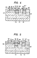
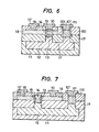
- FIGS 4 to 7 are sectional views showing different embodiments of the present invention, respectively.
- Figure 2 is a sectional view showing the essential portions of an embodiment of the present invention.
- the bipolar transistor of Figure 2 is a vertical n-p-n bipolar transistor which includes a collector 13, a base 14 and an emitter 15.
- a base electrode 10' is connected to a side part of the base 14 through a polycrystalline silicon film 18, while an emitter electrode 10 is connected directly on the emitter 15.
- an epitaxial silicon layer 111 is interposed between a collector electrode 10" and an n -type buried layer 12.
- a third insulating film (Si0 2 film) 110 is deposited on the exposed part of a first insulating film 17.
- the upper surface of the collector electrode 10" becomes even with the upper surfaces of the emitter electrode 10 and the base electrode 10', and also the upper surfaces of a second insulating film 19 and the third insulating film 110 become even.
- the bipolar transistor of the present invention has the steps reduced conspicuously and its topside flattened, so that the breaking of interconnections is feared much less. It is therefore possible to form the multi-level interconnections without anxiety.
- an n +- type buried layer 12 is formed on a p-type Si substrate 11 by a well-known expedient such as ion implantation and thermal diffusion, whereupon an epitaxial Si layer 13 is formed by the well-known vapor epitaxial growth technique.
- a well-known expedient such as ion implantation and thermal diffusion
- an epitaxial Si layer 13 is formed by the well-known vapor epitaxial growth technique.
- the exposed parts of the epitaxial Si layer 13' are etched and removed by the reactive ion etching by- employing the three layers of the insulating films 101, 102 and 103 as a mask.
- the etching may be performed until the buried layer 12 is exposed, or so that the epitaxial Si layer 13 is slightly left on the upper surface of the buried layer 12 as illustrated in Figure 3b.
- the parts of the epitaxial Si layer 13 underlying the three-layer insulating films 101, 102 and 103 are side-etched by the wet etching, to form structures in which the three-layer insulating films 101, 102 and 103 overhang.
- this step of side etching is not always indispensable, it should preferably be carried out because the overhang structures are effective for leaving an Si 3 N 4 film 105 on the side surfaces of parts of the epitaxial Si layer 13 in succeeding steps.
- An Si0 2 film 104 is formed on the upper surface of the epitaxial Si layer 13 and the surfaces of the overhang structure parts thereof by the well-known thermal oxidation, whereupon the Si 3 N 4 film 105 is further stacked and formed on the Si0 2 film 104 by the well-known CVD (chemical vapor deposition) process.
- CVD chemical vapor deposition
- the Si 3 N 4 film 105 deposited on parts other than the side surfaces of the three-layer insulating films 101, 102 and 103 and the parts of the epitaxial Si layer 13 underlying these insulating films is etched and removed, whereupon the exposed parts of the Si0 2 film 104 are further etched and removed.
- the Si0 2 film 104 and the Si 3 N 5 film 105 remain on the side surfaces of the overhang structure parts of the epitaxial layer 13, and the Si 3 N 4 film 105 remains on the side surfaces of the three-layer insulating films 101, 102 and 103.
- a thick Si0 2 film (having a thickness of about 1 f m) 17 is formed by the well-known thermal oxidation. Thereafter, the Si0 2 layer 104 and the Si 3 N 4 film 105 are etched and removed. A polycrystalline silicon film 18 is deposited on the whole area, and is thereafter patterned so as to remove its parts deposited on the remaining parts of the Si0 2 film 103. Thus, as illustrated in Figure 3c, a recess between the remaining parts of the epitaxial Si layer 13 is filled up with the polycrystalline silicon film 18.
- An Si0 2 film 104 and an Si 3 N 4 film 105 are stacked and deposited on the whole area. Thereafter, etching is performed so that, as illustrated in Figure 3d, the parts of the Si0 2 film 104 and the Si 3 N 4 film 105 deposited on regions to form an emitter electrode and a base lead-out electrode therein may be left behind, whereas the parts deposited on the other regions may be removed.
- the thermal oxidation is performed to oxidize the exposed parts of the polycrystalline silicon film 18 and to form an SiO 2 film 110.
- the SiO 2 film IO 4 and the Si 3 N 4 film 105 used as a mask in the above oxidizing step are removed to expose the upper surface of the polycrystalline silicon film 18.
- a p-type impurity is introduced into the exposed part of the polycrystalline silicon film 18 by the thermal diffusion or ion implantation, to turn the part into a low resistance. Thereafter, the surface of the polycrystalline silicon film 18 is oxidized to form an SiO 2 film 19. ( Figure 2)
- a base 14 and an emitter 15 are formed by a well-known method.
- the emitter electrode 10, base electrode 10' and collector electrode 10" made of conductive metal films of Al or the like are formed. Then, the n-p-n vertical bipolar transistor shown in Figure 2 is formed.
- the bipolar transistor of the embodiment has such other merits that, since the base-collector junction is small, the parasitic capacitance is low and a high switching speed is possible, and that, since the Si0 2 film 17 serves also for the isolation between the respectively adjacent transistors, any isolation means need not be added and the required area is small.
- An embodiment shown in Figure 4 is such that a polycrystalline silicon film 120 is interposed between an emitter 15 and an emitter electrode 10.
- the emitter 15 can be made as very thin as about 0.1 - 0.3 /m, so that a still higher switching operation is permitted.
- An embodiment shown in Figure 5 is such that a film 121 of a metal silicide, e. g., MoSi 2 is disposed on a polycrystalline silicon film 18.
- a metal silicide e. g., MoSi 2
- An embodiment shown in Figure 6 has a structure in which a stacked film 123 consisting of an Si0 2 film 104 and an Si 3 N 4 film 105 is left on the side surface of a collector leading-out epitaxial Si layer 111.
- the present invention is not restricted to such vertical transistors, but it is also applicable to a lateral transistor or to a semiconductor device in which a vertical transistor and a lateral transistor are formed on an identical semiconductor substrate.
- Figure ? shows an embodiment in which the present invention is applied to a lateral transistor.
- an emitter and a collector are led out by interconnections of a polycrystalline silicon film 18, and a base is led out by a buried layer 12 and an epitaxial Si layer of low resistance 111.
- the construction other than the collector 13, base 14 and emitter 15 is the same as in the case of the vertical transistor, and it can be formed by the same manufacturing steps as in the foregoing.
Landscapes
- Bipolar Transistors (AREA)
- Internal Circuitry In Semiconductor Integrated Circuit Devices (AREA)
- Bipolar Integrated Circuits (AREA)
Applications Claiming Priority (2)
| Application Number | Priority Date | Filing Date | Title |
|---|---|---|---|
| JP171443/81 | 1981-10-28 | ||
| JP56171443A JPS5873156A (ja) | 1981-10-28 | 1981-10-28 | 半導体装置 |
Publications (3)
| Publication Number | Publication Date |
|---|---|
| EP0078501A2 true EP0078501A2 (de) | 1983-05-11 |
| EP0078501A3 EP0078501A3 (en) | 1986-06-04 |
| EP0078501B1 EP0078501B1 (de) | 1989-08-30 |
Family
ID=15923205
Family Applications (1)
| Application Number | Title | Priority Date | Filing Date |
|---|---|---|---|
| EP82109931A Expired EP0078501B1 (de) | 1981-10-28 | 1982-10-27 | Transistorähnliche Halbleiteranordnung und Verfahren zu deren Herstellung |
Country Status (6)
| Country | Link |
|---|---|
| US (2) | US4825281A (de) |
| EP (1) | EP0078501B1 (de) |
| JP (1) | JPS5873156A (de) |
| KR (1) | KR900003835B1 (de) |
| CA (1) | CA1195435A (de) |
| DE (1) | DE3279918D1 (de) |
Cited By (8)
| Publication number | Priority date | Publication date | Assignee | Title |
|---|---|---|---|---|
| EP0102075A3 (en) * | 1982-08-30 | 1986-02-05 | Hitachi, Ltd. | Semiconductor device with a multilayer structure |
| EP0184016A1 (de) * | 1984-11-09 | 1986-06-11 | Hitachi, Ltd. | Bipolartransistor mit Heteroübergang |
| EP0118102A3 (en) * | 1983-03-07 | 1987-09-30 | Hitachi, Ltd. | Semiconductor device |
| EP0186578A3 (en) * | 1984-12-18 | 1988-01-07 | Thomson Components-Mostek Corporation | Bipolar microwave integratable transistor and method therefor |
| EP0251927A3 (en) * | 1986-07-02 | 1988-11-23 | Fairchild Semiconductor Corporation | Bipolar transistor with polysilicon stringer base contact |
| US4974046A (en) * | 1986-07-02 | 1990-11-27 | National Seimconductor Corporation | Bipolar transistor with polysilicon stringer base contact |
| US5063168A (en) * | 1986-07-02 | 1991-11-05 | National Semiconductor Corporation | Process for making bipolar transistor with polysilicon stringer base contact |
| WO1997047043A1 (en) * | 1996-06-06 | 1997-12-11 | The Whitaker Corporation | Reduced capacitance bipolar junction transistor |
Families Citing this family (8)
| Publication number | Priority date | Publication date | Assignee | Title |
|---|---|---|---|---|
| US5214302A (en) * | 1987-05-13 | 1993-05-25 | Hitachi, Ltd. | Semiconductor integrated circuit device forming on a common substrate MISFETs isolated by a field oxide and bipolar transistors isolated by a groove |
| JPH04314350A (ja) * | 1991-04-12 | 1992-11-05 | Hitachi Ltd | 半導体集積回路装置の製造方法 |
| KR100292330B1 (ko) * | 1992-05-01 | 2001-09-17 | 이데이 노부유끼 | 반도체장치와그제조방법및실리콘절연기판의제조방법 |
| GB2296377A (en) * | 1994-12-20 | 1996-06-26 | Korea Electronics Telecomm | Pillar bipolar transistors |
| FR2756100B1 (fr) | 1996-11-19 | 1999-02-12 | Sgs Thomson Microelectronics | Transistor bipolaire a emetteur inhomogene dans un circuit integre bicmos |
| FR2756103B1 (fr) * | 1996-11-19 | 1999-05-14 | Sgs Thomson Microelectronics | Fabrication de circuits integres bipolaires/cmos et d'un condensateur |
| FR2756974B1 (fr) * | 1996-12-10 | 1999-06-04 | Sgs Thomson Microelectronics | Transistor bipolaire a isolement par caisson |
| US6436770B1 (en) * | 2000-11-27 | 2002-08-20 | Chartered Semiconductor Manufacturing Ltd. | Method to control the channel length of a vertical transistor by first forming channel using selective epi and source/drain using implantation |
Family Cites Families (14)
| Publication number | Priority date | Publication date | Assignee | Title |
|---|---|---|---|---|
| US3716422A (en) * | 1970-03-30 | 1973-02-13 | Ibm | Method of growing an epitaxial layer by controlling autodoping |
| US4396933A (en) * | 1971-06-18 | 1983-08-02 | International Business Machines Corporation | Dielectrically isolated semiconductor devices |
| US3796613A (en) * | 1971-06-18 | 1974-03-12 | Ibm | Method of forming dielectric isolation for high density pedestal semiconductor devices |
| JPS5197385A (en) * | 1975-02-21 | 1976-08-26 | Handotaisochino seizohoho | |
| US4099987A (en) * | 1977-07-25 | 1978-07-11 | International Business Machines Corporation | Fabricating integrated circuits incorporating high-performance bipolar transistors |
| DE2815605C3 (de) * | 1978-04-11 | 1981-04-16 | Siemens AG, 1000 Berlin und 8000 München | Halbleiterspeicher mit Ansteuerleitungen hoher Leitfähigkeit |
| US4276557A (en) * | 1978-12-29 | 1981-06-30 | Bell Telephone Laboratories, Incorporated | Integrated semiconductor circuit structure and method for making it |
| US4252581A (en) * | 1979-10-01 | 1981-02-24 | International Business Machines Corporation | Selective epitaxy method for making filamentary pedestal transistor |
| JPS5673446A (en) * | 1979-11-21 | 1981-06-18 | Chiyou Lsi Gijutsu Kenkyu Kumiai | Manufacture of semiconductor device |
| US4303933A (en) * | 1979-11-29 | 1981-12-01 | International Business Machines Corporation | Self-aligned micrometer bipolar transistor device and process |
| US4338138A (en) * | 1980-03-03 | 1982-07-06 | International Business Machines Corporation | Process for fabricating a bipolar transistor |
| US4309812A (en) * | 1980-03-03 | 1982-01-12 | International Business Machines Corporation | Process for fabricating improved bipolar transistor utilizing selective etching |
| US4319932A (en) * | 1980-03-24 | 1982-03-16 | International Business Machines Corporation | Method of making high performance bipolar transistor with polysilicon base contacts |
| US4378630A (en) * | 1980-05-05 | 1983-04-05 | International Business Machines Corporation | Process for fabricating a high performance PNP and NPN structure |
-
1981
- 1981-10-28 JP JP56171443A patent/JPS5873156A/ja active Pending
-
1982
- 1982-10-21 US US06/435,552 patent/US4825281A/en not_active Expired - Fee Related
- 1982-10-23 KR KR8204754A patent/KR900003835B1/ko not_active Expired
- 1982-10-27 DE DE8282109931T patent/DE3279918D1/de not_active Expired
- 1982-10-27 CA CA000414292A patent/CA1195435A/en not_active Expired
- 1982-10-27 EP EP82109931A patent/EP0078501B1/de not_active Expired
-
1990
- 1990-03-26 US US07/498,489 patent/US5061645A/en not_active Expired - Fee Related
Cited By (8)
| Publication number | Priority date | Publication date | Assignee | Title |
|---|---|---|---|---|
| EP0102075A3 (en) * | 1982-08-30 | 1986-02-05 | Hitachi, Ltd. | Semiconductor device with a multilayer structure |
| EP0118102A3 (en) * | 1983-03-07 | 1987-09-30 | Hitachi, Ltd. | Semiconductor device |
| EP0184016A1 (de) * | 1984-11-09 | 1986-06-11 | Hitachi, Ltd. | Bipolartransistor mit Heteroübergang |
| EP0186578A3 (en) * | 1984-12-18 | 1988-01-07 | Thomson Components-Mostek Corporation | Bipolar microwave integratable transistor and method therefor |
| EP0251927A3 (en) * | 1986-07-02 | 1988-11-23 | Fairchild Semiconductor Corporation | Bipolar transistor with polysilicon stringer base contact |
| US4974046A (en) * | 1986-07-02 | 1990-11-27 | National Seimconductor Corporation | Bipolar transistor with polysilicon stringer base contact |
| US5063168A (en) * | 1986-07-02 | 1991-11-05 | National Semiconductor Corporation | Process for making bipolar transistor with polysilicon stringer base contact |
| WO1997047043A1 (en) * | 1996-06-06 | 1997-12-11 | The Whitaker Corporation | Reduced capacitance bipolar junction transistor |
Also Published As
| Publication number | Publication date |
|---|---|
| KR900003835B1 (ko) | 1990-06-02 |
| JPS5873156A (ja) | 1983-05-02 |
| CA1195435A (en) | 1985-10-15 |
| EP0078501B1 (de) | 1989-08-30 |
| EP0078501A3 (en) | 1986-06-04 |
| KR840002162A (ko) | 1984-06-11 |
| US4825281A (en) | 1989-04-25 |
| US5061645A (en) | 1991-10-29 |
| DE3279918D1 (en) | 1989-10-05 |
Similar Documents
| Publication | Publication Date | Title |
|---|---|---|
| US4089021A (en) | Semiconductor device capable of withstanding high voltage and method of manufacturing same | |
| US3954523A (en) | Process for fabricating devices having dielectric isolation utilizing anodic treatment and selective oxidation | |
| US4892837A (en) | Method for manufacturing semiconductor integrated circuit device | |
| EP0083816B1 (de) | Halbleiteranordnung mit einem Verbindungsmuster | |
| US4641416A (en) | Method of making an integrated circuit structure with self-aligned oxidation to isolate extrinsic base from emitter | |
| EP0078501B1 (de) | Transistorähnliche Halbleiteranordnung und Verfahren zu deren Herstellung | |
| EP0021403A1 (de) | Selbstjustierende Halbleiterschaltungen | |
| US3873989A (en) | Double-diffused, lateral transistor structure | |
| US4425379A (en) | Polycrystalline silicon Schottky diode array | |
| JPH0123949B2 (de) | ||
| US4615746A (en) | Method of forming isolated island regions in a semiconductor substrate by selective etching and oxidation and devices formed therefrom | |
| JPS62211917A (ja) | P型領域に低抵抗オ−ム接点を形成する方法 | |
| US6087708A (en) | Semiconductor integrated circuit device and a method of producing the same | |
| US4407059A (en) | Method of producing semiconductor device | |
| US4746623A (en) | Method of making bipolar semiconductor device with wall spacer | |
| US4628339A (en) | Polycrystalline silicon Schottky diode array | |
| US4926235A (en) | Semiconductor device | |
| EP0036620B1 (de) | Halbleiterbauelement und Verfahren zu seiner Herstellung | |
| US4609414A (en) | Emitter finger structure in a switching transistor | |
| EP0246682A1 (de) | Verfahren zur Herstellung einer Halbleiteranordnung mit einer Elektrode aus polykristallinem Silizium | |
| EP0367293A2 (de) | Halbleiteranordnung mit selbstausgerichteter Basis und Verfahren zur Herstellung | |
| JP2579999B2 (ja) | 半導体装置の製造方法 | |
| JP3173184B2 (ja) | 半導体装置 | |
| JPH0157506B2 (de) | ||
| JPH05275633A (ja) | 半導体装置及びその製造方法 |
Legal Events
| Date | Code | Title | Description |
|---|---|---|---|
| PUAI | Public reference made under article 153(3) epc to a published international application that has entered the european phase |
Free format text: ORIGINAL CODE: 0009012 |
|
| AK | Designated contracting states |
Designated state(s): DE FR GB IT NL |
|
| PUAL | Search report despatched |
Free format text: ORIGINAL CODE: 0009013 |
|
| AK | Designated contracting states |
Kind code of ref document: A3 Designated state(s): DE FR GB IT NL |
|
| 17P | Request for examination filed |
Effective date: 19860618 |
|
| 17Q | First examination report despatched |
Effective date: 19870924 |
|
| GRAA | (expected) grant |
Free format text: ORIGINAL CODE: 0009210 |
|
| AK | Designated contracting states |
Kind code of ref document: B1 Designated state(s): DE FR GB IT NL |
|
| REF | Corresponds to: |
Ref document number: 3279918 Country of ref document: DE Date of ref document: 19891005 |
|
| ET | Fr: translation filed | ||
| ITF | It: translation for a ep patent filed | ||
| PLBE | No opposition filed within time limit |
Free format text: ORIGINAL CODE: 0009261 |
|
| STAA | Information on the status of an ep patent application or granted ep patent |
Free format text: STATUS: NO OPPOSITION FILED WITHIN TIME LIMIT |
|
| 26N | No opposition filed | ||
| ITTA | It: last paid annual fee | ||
| PGFP | Annual fee paid to national office [announced via postgrant information from national office to epo] |
Ref country code: FR Payment date: 19931018 Year of fee payment: 12 |
|
| PGFP | Annual fee paid to national office [announced via postgrant information from national office to epo] |
Ref country code: GB Payment date: 19931019 Year of fee payment: 12 |
|
| PGFP | Annual fee paid to national office [announced via postgrant information from national office to epo] |
Ref country code: NL Payment date: 19931031 Year of fee payment: 12 |
|
| PGFP | Annual fee paid to national office [announced via postgrant information from national office to epo] |
Ref country code: DE Payment date: 19931228 Year of fee payment: 12 |
|
| PG25 | Lapsed in a contracting state [announced via postgrant information from national office to epo] |
Ref country code: GB Effective date: 19941027 |
|
| PG25 | Lapsed in a contracting state [announced via postgrant information from national office to epo] |
Ref country code: NL Effective date: 19950501 |
|
| NLV4 | Nl: lapsed or anulled due to non-payment of the annual fee | ||
| GBPC | Gb: european patent ceased through non-payment of renewal fee |
Effective date: 19941027 |
|
| PG25 | Lapsed in a contracting state [announced via postgrant information from national office to epo] |
Ref country code: FR Effective date: 19950630 |
|
| PG25 | Lapsed in a contracting state [announced via postgrant information from national office to epo] |
Ref country code: DE Effective date: 19950701 |
|
| REG | Reference to a national code |
Ref country code: FR Ref legal event code: ST |