EP0078511B2 - Commutateur électronique de proximité - Google Patents
Commutateur électronique de proximité Download PDFInfo
- Publication number
- EP0078511B2 EP0078511B2 EP19820109985 EP82109985A EP0078511B2 EP 0078511 B2 EP0078511 B2 EP 0078511B2 EP 19820109985 EP19820109985 EP 19820109985 EP 82109985 A EP82109985 A EP 82109985A EP 0078511 B2 EP0078511 B2 EP 0078511B2
- Authority
- EP
- European Patent Office
- Prior art keywords
- transistor
- voltage
- circuit
- resistor
- capacitor
- Prior art date
- Legal status (The legal status is an assumption and is not a legal conclusion. Google has not performed a legal analysis and makes no representation as to the accuracy of the status listed.)
- Expired - Lifetime
Links
Images


Classifications
-
- H—ELECTRICITY
- H03—ELECTRONIC CIRCUITRY
- H03K—PULSE TECHNIQUE
- H03K17/00—Electronic switching or gating, i.e. not by contact-making and –breaking
- H03K17/94—Electronic switching or gating, i.e. not by contact-making and –breaking characterised by the way in which the control signals are generated
- H03K17/945—Proximity switches
- H03K17/95—Proximity switches using a magnetic detector
- H03K17/952—Proximity switches using a magnetic detector using inductive coils
- H03K17/9537—Proximity switches using a magnetic detector using inductive coils in a resonant circuit
- H03K17/9542—Proximity switches using a magnetic detector using inductive coils in a resonant circuit forming part of an oscillator
- H03K17/9547—Proximity switches using a magnetic detector using inductive coils in a resonant circuit forming part of an oscillator with variable amplitude
-
- H—ELECTRICITY
- H03—ELECTRONIC CIRCUITRY
- H03K—PULSE TECHNIQUE
- H03K17/00—Electronic switching or gating, i.e. not by contact-making and –breaking
- H03K17/94—Electronic switching or gating, i.e. not by contact-making and –breaking characterised by the way in which the control signals are generated
- H03K17/945—Proximity switches
- H03K17/95—Proximity switches using a magnetic detector
- H03K17/951—Measures for supplying operating voltage to the detector circuit
Definitions
- the invention relates to an electronic proximity switch with a voltage supply connected in series with the load and a control circuit which short-circuits the series circuit, an electronic switch and a supply circuit for generating an auxiliary voltage for the response circuit, consisting of an electronic circuit lying parallel to the voltage feed of the response circuit Voltage regulator, with the series connection of capacitor and voltage regulator lying parallel to the electronic switch.
- a known proximity switch of the type mentioned above (DE-OS 24 35 501) the electronic switch, in this case a thyristor or triac, is operated with a phase angle greater than zero and an auxiliary voltage for the oscillator is derived both in the conductive and in the blocked state and kept constant by a controller.
- this known proximity switch there is neither a phase angle control dependent on the capacitor voltage nor a direct control connection to the electronic switch.
- the invention is therefore based on the object of providing a proximity switch which is versatile in relation to the supply voltage with a relatively low voltage and low losses.
- a proximity switch of the above-mentioned type in a simple manner in that the voltage supply is designed as a continuous DC voltage, that a comparison circuit detecting the capacitor voltage is in operative connection with the control connection of the electronic switch designed as a transistor and the comparison circuit when the value falls below a predetermined lower level Capacitor voltage blocks the transistor until a predetermined upper capacitor voltage is reached.
- the comparison circuit is provided with a hysteresis circuit.
- the comparison circuit consists of a series connection of resistor, Zener diode and base-emitter path of the transistor, the emitter-collector path of which is connected in series by a further resistor with the emitter-base path of a second transistor.
- parallel to the further resistor is the emitter-base path of an output transistor, the collector of which is at the control input of the transistor and the collector of which is connected to the base of the further transistor and this connection point is connected to a resistor at the input of the comparison circuit, which in turn is connected via a resistor to the collector of the further transistor, this connection point being connected via a resistor at the connection point between the resistor and the Zener diode.
- An additional voltage standard in the form of the Zener diode for the voltage regulator can be dispensed with if the comparative circuit aging is on the one hand at the base of a transistor forming the voltage regulator and on the other hand at the negative pole of the supply circuit.
- a diode is connected between the voltage regulator and the transistor and the connection point to the voltage regulator is routed to the outside.
- a luminescent diode (LED) with a parallel resistor is connected between the diode and the voltage regulator
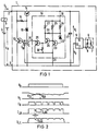
- the circuit of the proximity switch 1 shown in FIG. 1 has terminals 2 and 3, to which a voltage source 4 and a load 5, for example a relay, are connected.
- a detection circuit 6 consists of the response coil 7 and the capacitor 8.
- the response coil 7 and the capacitor 8 as well as voltage supply terminals 10 and 11 are connected to a response circuit 9.
- the control output is designated 12.
- a transistor 13 is connected to the terminals 2 and 3 of the proximity switch 1 with the collector and the emitter.
- the base of the transistor is connected to the control output 12 of the response circuit 9.
- the collector of transistor 14 together with one terminal of resistor 15 is also at terminal 2.
- the base of transistor 14 with the other terminal of resistor 15 is at the cathode of constant voltage element 16, a zener diode, and its emitter is at voltage supply terminal 10 of the response circuit 9.
- the anode of the constant voltage element 16 is connected to the terminal 3.
- a capacitor 17 is connected between the voltage supply terminals 10, 11 of the address circuit 9. 1 shows a comparison circuit 18 which is connected to the voltage input terminal 19 on the positive side of the capacitor 17.
- An output terminal 20 is located at the base of transistor 13 and the negative terminal 21 is located at terminal 3.
- the anode of a constant voltage element 22 is connected to the base of transistor 23, the cathode is connected to voltage input terminal 19 via resistor 24.
- the emitter of transistor 23 is connected to terminal 21 and its collector to voltage input terminal 19 via resistor 25 and at the same time to the base of transistor 26.
- the collector of transistor 26 is connected to terminal 19 via resistor 27 and to the cathode of constant voltage element 22 via resistor 28
- the emitter of transistor 26 is connected to the base of transistor 29 and to terminal 21 via resistor 30.
- the collector of transistor 29 is connected to output terminal 20 and its emitter to minus terminal 21.
- the block voltage of the series circuit which consists of the constant voltage element 22 of the base-emitter path of the transistor 23, will be slightly smaller than the nominal voltage of the constant voltage element 16, so that when the transistor 13 is in the off state, because the Object to be monitored is located far away from the response coil 7, the voltage applied to the voltage input terminal 19 exceeds the block voltage in order to make the transistor 23 conductive, so that the transistors 26 and 29 depending on the transistor 23 enter the exhibition.
- the terminal voltage V c becomes lower than the block voltage in the series circuit, which consists of the series connection of the constant voltage element 22 of the comparison circuit 18 and the base-emitter path of the transistor 23.
- the transistor 23 goes into the blocking state.
- transistors 26, 29 go into the conductive state.
- the collector voltage of the transistor 14 is restored and the current flows through the capacitor 17 and the voltage supply terminal 10 of the response circuit 9 through the collector-emitter path of the transistor.
- the terminal voltage of the capacitor 17 increases in accordance with the time constant, which depends on the capacitance of the capacitor and the resistance of the load 5, the transistor 14, the response circuit 9, the comparison circuit 18 and others.
- the voltage V c of the capacitor 17 has again reached a predeterminable value, current flows to the base of the transistor 23, which in turn becomes conductive.
- the transistors 26 and 29 cease to be conductive depending on the transistor, whereby the current which originates from the control output 12 of the response circuit and has a bypass through the transistor 29 can flow back to the base of the transistor 13. As soon as this transistor conducts, the transistor 14 comes into the blocking state, which is repeated several times.
- the comparison circuit 18 is equipped with a hysteresis.
- the transistor 26 conducts depending on the transistor 23 which has not become conductive, the collector current flows not only through the resistor 27, but also through the resistors 24 and 28. Accordingly, if the terminal voltage V c of the capacitor 17 to a voltage has increased, which causes the transistor 23 to switch off - this is the so-called block voltage (lower limit value V c u on the series circuit, consisting of the constant voltage element 22 and the base-emitter path of the transistor 23-, the transistor 23 does not become conductive before the terminal voltage V c of the capacitor 17 has risen to a voltage value (upper limit value V CH ), which consists of an average of the lower limit value V CL and a voltage drop across the resistor 24
- the comparison circuit 18 makes the transistor 29 conductive when the voltage applied to the voltage input terminal 19 is lower than the lower limit value V CL and switches the transistor 29 off when the voltage applied to the terminal 19 has risen to the upper limit value V cH is.
- the comparison circuit 18 has a hysteresis character. Because of this hysteresis nature, the comparison circuit 18 operates intermittently to temporarily turn off the transistor 13 so that the capacitor 17 is charged when the terminal voltage V c on the capacitor 17 drops below the lower limit value V cL after the transistor 13 has been conducting and the transistor 13 to enable the current flow again at a time when the terminal voltage V c has again reached the upper limit value V cH .
- I LR is the current that flows when the load 5 is a resistive load, the level of the charging current being determined by the resistance value of the load 5 and that between the collector and emitter of the transistor 14 when it is conductive.
- the current flows into the capacitor 17 during the charging period t.
- This charging current I LRC is slightly smaller than the current I LR when the transistor 13 is conductive, so that the load 5 remains addressed even in the period t.
- I LL indicates the current that flows in the load 5 if it is inductive and the current I LLC, which is almost equal to the current I LL that flows due to the magnetic energy in the load 5 when the transistor 13 is conductive, ensures that the load 5 remains in operation.
- FIG. 3 shows another example of the present invention.
- the constant voltage element 16 is omitted in the constant voltage circuit according to FIG. 2.
- the voltage input terminal 19 of the comparison circuit 18 is connected to the base of the transistor 14.
- the constant voltage element 22 for voltage detection within the comparison circuit 18 can also be used as a constant voltage element in the constant voltage circuit.
- the change in the terminal voltage Vc of the capacitor 17 is derived indirectly from the base potential of the capacitor 17.
- the applied voltage between the terminals of the switch according to the present invention can be reduced to a minimum when the switch is conductive, and consequently the amount of current flow in the load can be adjusted almost to the value that with an ideal switch is achievable in terms of contact.
- inductive switches it is readily possible to apply the subject matter of the invention to capacitive or photoelectric direct current two-wire proximity switches.
- Fig. 4 shows a further circuit variant of the proximity switch according to the invention.
- the proximity switch has another one, which is designated by 31.
- the voltage source 4 is connected between the terminals 3 and 31 and the load 5 between the terminals 2 and 31 in a three-wire system, and the series connection of voltage source 4 and load 5 is between the terminals 2 and 3, the terminal 31 being left open or is connected to terminal 2 if a two-wire system is required.
- the power supply from the terminal 2 to the response circuit 9, the constant voltage element 16 and the capacitor 17 takes place via a diode 32 which is switched on in the forward direction with the transistor 14.
- the connection point between the cathode of the diode 32 and the collector of the transistor 14 is led to the terminal 31.
- the function of the two-wire proximity switch is essentially the same as the function of the switch shown in FIG. 1. It is apparent that the function is exactly equivalent in the case when the terminals 2 and 31 are short-circuited.
- the proximity switch is connected as a three-wire switch, as indicated by the dashed line 33 in Fig. 4, the current from the voltage source 4 to the response circuit 9 via a constant voltage circuit consisting of the transistor 14, the constant voltage element 16 and led to the resistor 15, the voltage essentially depends on the terminal voltage of the constant voltage element 16.
- transistor 13 is in the setting, current flow from voltage source 4 to transistor 13 via diode 32 is prevented.
- the constant voltage circuit transistor 14, constant voltage element 16 and resistor 15
- the transistor 29 of the comparison circuit 18 does not switch accordingly, because the voltage at response circuit 9 is higher is than the threshold voltage of the comparison circuit 18.
- the transistor 13 can remain in constant setting and as a result no voltage loss occurs on the way between the terminals 2 and 3, seen from the voltage source 4, the clamping in comparison to the two-wire version can be considerable can be reduced. As soon as the transistor 13 turns off, the diode 32 can continue to act as a freewheeling diode. In the case in which the load is an inductive load, the current in the load 5 can continue to flow, so that excessive voltages on the transistor 13 are thereby avoided.
- the leakage current in the load 5 can be considerably reduced compared to the two-wire connection in which the current for the response circuit 9 is generated by the load 5; because in the present case only the leakage current of the transistor 13 flows through the load 5 and all other currents which are required by the response circuit 9, the comparison circuit 18 are brought in via the terminal 31.
- FIG. 5 shows a further embodiment of the invention, in which an LED diode (light-emitting diode) is provided for displaying the operating conditions.
- the LED 34 is turned on in the forward direction between the terminal 31 and the collector of the transistor 14, in parallel with a resistor 35.
- a resistor 36 is on the one hand at the connection point of the cathode of the LED 34 and the collector of the transistor 14 and on the other hand at the collector of the transistor 13. If the two-wire version is considered in such a circuit arrangement, current flows through the response circuit 9 and the comparison circuit 18 via a parallel connection from the LED 34 and the resistor 35 when the transistor 13 is in the off state.
- the voltage drop across the resistor 35 is smaller than the forward voltage of the LED, so that the LED 34 is not switched on. Since a pulse-like voltage can be present at the response circuit 9 and the comparison circuit 18 when the transistor 13 turns off, the peak value of the current flowing through the resistor 35 and the LED 34 turns the LED on.
- the LED 34 is not turned on by the bypass resistor 35 when the transistor 13 turns off, as is the case in the two-wire version.
- transistor 13 turns on, to turn on LED 34, current will flow in the following way: voltage source 4, terminal 31, LED 34, resistor 36, transistor 13.
- the comparison circuit 18 is in the arrangement as shown in FIG 4 and 5 is shown, can be carried out exactly as it was generated in Fig. 1 or 3.
- the arrangement according to the invention can be used in a three-wire version without the Impair the function of the proximity switch in two-wire version. Accordingly, the switch can be used in both two-wire and three-wire systems.
- a proximity switch with a two-wire system of known design has the disadvantage that, compared to a proximity switch with a three-wire design, there is a greater leakage current, since the power supply via the load to the response circuit must also take place when the output is interrupted. It is also disadvantageous that the on-voltage, which is necessary to make the path between the two terminals 2 and 3 conductive by repeated switching on and off of the transistor 13, is higher, since current to the response circuit in the conductive state of the Output must be performed.
Landscapes
- Electronic Switches (AREA)
Claims (6)
Applications Claiming Priority (4)
| Application Number | Priority Date | Filing Date | Title |
|---|---|---|---|
| JP174009/81 | 1981-10-30 | ||
| JP17400981A JPS5875925A (ja) | 1981-10-30 | 1981-10-30 | 近接スイツチ |
| JP56188364A JPS5890827A (ja) | 1981-11-26 | 1981-11-26 | 直流2線式近接スイツチ |
| JP188364/81 | 1981-11-26 |
Publications (4)
| Publication Number | Publication Date |
|---|---|
| EP0078511A2 EP0078511A2 (fr) | 1983-05-11 |
| EP0078511A3 EP0078511A3 (en) | 1984-10-10 |
| EP0078511B1 EP0078511B1 (fr) | 1987-08-19 |
| EP0078511B2 true EP0078511B2 (fr) | 1991-08-07 |
Family
ID=26495770
Family Applications (1)
| Application Number | Title | Priority Date | Filing Date |
|---|---|---|---|
| EP19820109985 Expired - Lifetime EP0078511B2 (fr) | 1981-10-30 | 1982-10-28 | Commutateur électronique de proximité |
Country Status (2)
| Country | Link |
|---|---|
| EP (1) | EP0078511B2 (fr) |
| DE (1) | DE3277051D1 (fr) |
Families Citing this family (4)
| Publication number | Priority date | Publication date | Assignee | Title |
|---|---|---|---|---|
| IT1215279B (it) * | 1985-06-10 | 1990-01-31 | Ates Componenti Elettron | Dispositivo elettrico di potenza intelligente a circuito integrato monolitico. |
| DE4114835A1 (de) * | 1991-05-07 | 1992-11-12 | Vdo Schindling | Schalteinrichtung, insbesondere zur verwendung in kraftfahrzeugen |
| GB2262998B (en) * | 1991-12-31 | 1995-10-25 | Square D Co | Improvements in and relating to proximity switches |
| DE102007034270A1 (de) * | 2007-07-19 | 2009-01-22 | Siemens Ag | Schaltungsanordnung mit einer mit einem Oszillator verbundenen Spule sowie Verfahren zum Betreiben einer solchen Schaltungsanordnung |
Family Cites Families (4)
| Publication number | Priority date | Publication date | Assignee | Title |
|---|---|---|---|---|
| US3524997A (en) * | 1967-09-08 | 1970-08-18 | Gen Electric | Monolithic integrated phase control circuits |
| DE2435501B2 (de) * | 1974-07-24 | 1976-05-20 | Pulsotronic Merten Kg, 5270 Gummersbach | Zweipoliges, beruehrungslos wirkendes schaltgeraet |
| DE2616265B2 (de) * | 1976-04-13 | 1978-09-28 | Robert 7995 Neukirch Buck | Elektronisches Schaltgerät |
| FR2368049A1 (fr) * | 1976-10-15 | 1978-05-12 | Itt Produits Ind | Detecteur de proximite |
-
1982
- 1982-10-28 EP EP19820109985 patent/EP0078511B2/fr not_active Expired - Lifetime
- 1982-10-28 DE DE8282109985T patent/DE3277051D1/de not_active Expired
Also Published As
| Publication number | Publication date |
|---|---|
| DE3277051D1 (en) | 1987-09-24 |
| EP0078511A3 (en) | 1984-10-10 |
| EP0078511A2 (fr) | 1983-05-11 |
| EP0078511B1 (fr) | 1987-08-19 |
Similar Documents
| Publication | Publication Date | Title |
|---|---|---|
| DE2747607C2 (de) | Schaltungsanordnung zur Ansteuerung eines bistabilen Relais | |
| DE2549586B2 (de) | Zündeinrichtung für Brennkraftmaschinen | |
| DE1095879B (de) | Transistor-Verzoegerungsstromkreis | |
| DE3151174C2 (de) | Überstrom-Schutzvorrichtung für einen Gleichstrommotor | |
| DE2205543A1 (de) | Anordnung zur spannungsversorgung eines zum anschluss an eine brennstoffbatterie bestimmten laststromkreises | |
| DE2753869C2 (de) | Meßwertgeber | |
| DE2907673A1 (de) | Schaltungsanordnung zur ansteuerung eines bistabilen relais | |
| DE2347483C3 (de) | Sperrschwinger | |
| EP0219074B1 (fr) | Commutateur du type à deux fils avec un transistor de puissance | |
| EP0080462B1 (fr) | Circuit commutateur semiconducteur pour charge inductive | |
| EP0078511B1 (fr) | Commutateur électronique de proximité | |
| DE1763492C3 (de) | Fühleinrichtung für die Strombegrenzungseinrichtung einer Regeleinrichtung | |
| DE2914593C2 (de) | Erdschlußdetektor | |
| DE2747416C2 (fr) | ||
| DE1513375C3 (de) | Schaltungsanordnung zum Verhindern zu weitgehender Entladungen einer als Energiequelle verwendeten Batterie | |
| DE2126428B2 (de) | Batteriegespeistes Transistorzündsystem für Brennkraftmaschinen | |
| CH663077A5 (de) | Selbstueberwachender flammenwaechter. | |
| DE3432567C1 (de) | Schaltungsanordnung zur Kurzschlußüberwachung | |
| DE1563840B2 (de) | Automatische Spüleinrichtung für sanitäre Anlagen mit elektrischer Steuerung | |
| DE1788003C3 (de) | Elektrische Schaltungsanordnung zur Zweipunktregelung eines eine induktive Last durchfließenden Stromes | |
| DE1933862B2 (de) | Mit wechselstrom betriebene verzoegerungsschaltungsanordnung | |
| DE3044842C2 (de) | Verfahren zum Einschalten von im Schaltbetrieb arbeitenden Leistungstransistoren und Schaltungsanordnungen zur Durchführung des Verfahrens | |
| DE2544482C3 (de) | Aus einer Strom- und Spannungsbegrenzungsschaltung bestehende Zenerbarriere | |
| DE2101441C (fr) | ||
| DE2415629B2 (de) | Schaltungsanordnung zum zeitweiligen, von der Größe der veränderlichen Betriebsspannung abhangigen Blockieren eines Stromzweiges |
Legal Events
| Date | Code | Title | Description |
|---|---|---|---|
| PUAI | Public reference made under article 153(3) epc to a published international application that has entered the european phase |
Free format text: ORIGINAL CODE: 0009012 |
|
| AK | Designated contracting states |
Designated state(s): CH DE FR GB IT LI |
|
| PUAL | Search report despatched |
Free format text: ORIGINAL CODE: 0009013 |
|
| AK | Designated contracting states |
Designated state(s): CH DE FR GB IT LI |
|
| 17P | Request for examination filed |
Effective date: 19850328 |
|
| 17Q | First examination report despatched |
Effective date: 19860515 |
|
| GRAA | (expected) grant |
Free format text: ORIGINAL CODE: 0009210 |
|
| AK | Designated contracting states |
Kind code of ref document: B1 Designated state(s): CH DE FR GB IT LI |
|
| REF | Corresponds to: |
Ref document number: 3277051 Country of ref document: DE Date of ref document: 19870924 |
|
| ET | Fr: translation filed | ||
| ITF | It: translation for a ep patent filed | ||
| PLBI | Opposition filed |
Free format text: ORIGINAL CODE: 0009260 |
|
| 26 | Opposition filed |
Opponent name: GEBHARD BALLUFF FABRIK FEINMECHANISCHER ERZEUGNISS Effective date: 19880519 |
|
| PUAH | Patent maintained in amended form |
Free format text: ORIGINAL CODE: 0009272 |
|
| STAA | Information on the status of an ep patent application or granted ep patent |
Free format text: STATUS: PATENT MAINTAINED AS AMENDED |
|
| 27A | Patent maintained in amended form |
Effective date: 19910807 |
|
| AK | Designated contracting states |
Kind code of ref document: B2 Designated state(s): CH DE FR GB IT LI |
|
| REG | Reference to a national code |
Ref country code: CH Ref legal event code: AEN |
|
| ET3 | Fr: translation filed ** decision concerning opposition | ||
| ITTA | It: last paid annual fee | ||
| ITF | It: translation for a ep patent filed | ||
| PGFP | Annual fee paid to national office [announced via postgrant information from national office to epo] |
Ref country code: CH Payment date: 19960118 Year of fee payment: 14 |
|
| PGFP | Annual fee paid to national office [announced via postgrant information from national office to epo] |
Ref country code: GB Payment date: 19960919 Year of fee payment: 15 |
|
| PGFP | Annual fee paid to national office [announced via postgrant information from national office to epo] |
Ref country code: FR Payment date: 19961025 Year of fee payment: 15 |
|
| PG25 | Lapsed in a contracting state [announced via postgrant information from national office to epo] |
Ref country code: LI Effective date: 19961031 Ref country code: CH Effective date: 19961031 |
|
| PGFP | Annual fee paid to national office [announced via postgrant information from national office to epo] |
Ref country code: DE Payment date: 19961216 Year of fee payment: 15 |
|
| REG | Reference to a national code |
Ref country code: CH Ref legal event code: PL |
|
| PG25 | Lapsed in a contracting state [announced via postgrant information from national office to epo] |
Ref country code: GB Free format text: LAPSE BECAUSE OF NON-PAYMENT OF DUE FEES Effective date: 19971028 |
|
| PG25 | Lapsed in a contracting state [announced via postgrant information from national office to epo] |
Ref country code: FR Free format text: THE PATENT HAS BEEN ANNULLED BY A DECISION OF A NATIONAL AUTHORITY Effective date: 19971031 |
|
| GBPC | Gb: european patent ceased through non-payment of renewal fee |
Effective date: 19971028 |
|
| PG25 | Lapsed in a contracting state [announced via postgrant information from national office to epo] |
Ref country code: DE Free format text: LAPSE BECAUSE OF NON-PAYMENT OF DUE FEES Effective date: 19980701 |
|
| REG | Reference to a national code |
Ref country code: FR Ref legal event code: ST |