EP0078577A1 - Générateur de code - Google Patents
Générateur de code Download PDFInfo
- Publication number
- EP0078577A1 EP0078577A1 EP82201355A EP82201355A EP0078577A1 EP 0078577 A1 EP0078577 A1 EP 0078577A1 EP 82201355 A EP82201355 A EP 82201355A EP 82201355 A EP82201355 A EP 82201355A EP 0078577 A1 EP0078577 A1 EP 0078577A1
- Authority
- EP
- European Patent Office
- Prior art keywords
- signal
- code
- code generator
- summing network
- value
- Prior art date
- Legal status (The legal status is an assumption and is not a legal conclusion. Google has not performed a legal analysis and makes no representation as to the accuracy of the status listed.)
- Granted
Links
- 230000005540 biological transmission Effects 0.000 claims abstract description 16
- 230000003111 delayed effect Effects 0.000 description 4
- 238000001228 spectrum Methods 0.000 description 4
- 230000035945 sensitivity Effects 0.000 description 2
- 238000005513 bias potential Methods 0.000 description 1
- 239000003990 capacitor Substances 0.000 description 1
- 238000010586 diagram Methods 0.000 description 1
- 230000000717 retained effect Effects 0.000 description 1
- 230000003595 spectral effect Effects 0.000 description 1
- 230000001360 synchronised effect Effects 0.000 description 1
Images

Classifications
-
- H—ELECTRICITY
- H04—ELECTRIC COMMUNICATION TECHNIQUE
- H04L—TRANSMISSION OF DIGITAL INFORMATION, e.g. TELEGRAPHIC COMMUNICATION
- H04L25/00—Baseband systems
- H04L25/38—Synchronous or start-stop systems, e.g. for Baudot code
- H04L25/40—Transmitting circuits; Receiving circuits
- H04L25/49—Transmitting circuits; Receiving circuits using code conversion at the transmitter; using predistortion; using insertion of idle bits for obtaining a desired frequency spectrum; using three or more amplitude levels ; Baseband coding techniques specific to data transmission systems
- H04L25/4917—Transmitting circuits; Receiving circuits using code conversion at the transmitter; using predistortion; using insertion of idle bits for obtaining a desired frequency spectrum; using three or more amplitude levels ; Baseband coding techniques specific to data transmission systems using multilevel codes
- H04L25/4923—Transmitting circuits; Receiving circuits using code conversion at the transmitter; using predistortion; using insertion of idle bits for obtaining a desired frequency spectrum; using three or more amplitude levels ; Baseband coding techniques specific to data transmission systems using multilevel codes using ternary codes
Definitions
- the invention relates to a code generator for producing a transmission code in response to an input serial binary code and to a data transmission system including such a code generator.
- the transmitted signal should have a small low frequency content and since the signal will normally be required to pass through transformers there should be no d.c. component.
- codes which have the property of suppressing the lower frequencies but the most effective is that known as WAL2 (or top-hat) which has a second order zero in its spectrum at zero frequency (d.c.) and consequently the smallest low-frequency energy.
- WAL2 or top-hat
- this code has a relatively large high frequency (greater than the bit frequency) content which leads to an increased sensitivity to crosstalk between different systems.
- the invention provides a code generator for producing a transmission code in response to an input serial binary code having a bit period T, the code generator comprising means for generating a signal having a first value for a period T/2 located centrally in the bit period in response to a bit of one binary state, means for generating a signal having a second value for the period T/2 in response to a bit of the other binary state, means for generating a signal having the second value during the interval between the T/2 periods of successive bits when two consecutive bits are of the one binary state, means for generating a signal having the first value during the interval between the T/2 periods of successive bits when two consecutive bits are of the other binary state, and means for producing a signal having a value intermediate the first and second values during the interval between the T/2 periods of successive bits when two consecutive bits are of different binary states.
- the code generator of the invention produces a transmission code in which the double frequency cycle produced by the WAL2 code when the binary input changes state is replaced by a steady signal located midway between the two extreme values. In this way the high frequency content of the signal is reduced.
- a further property of the code is that the transmitted power is 75% of the peak power whereas for WAL2 it is 100% of the peak power. This is as a result of holding the signal at zero level for the interval between a 1 and a 0 or vice versa. This interval is half a bit period and 50% of such intervals are zero.
- the main disadvantage is that the output is a three level signal and the encoder must have good linearity if the low frequency spectral characteristics is to be preserved.
- the code generator may comprise a first current source connected by a first switch to a summing network, a second current source connected by a second switch to the summing network, the first and second current sources producing substantially equal currents, and a control circuit for operating the first and second switches; wherein to produce a signal of the first value the control circuit produces signals to close the first and second switches so that both current sources are connected to the summing network, to produce a signal of the second value the control circuit produces signals to open the first and second switches so that both current sources are disconnected from the summing network, and to produce a signal having the intermediate value the control circuit produces signals to close one of the first and second switches and to open the other of the first and second switches so that one of the current sources is connected to the summing network while the other of the current sources is disconnected from the summing network.
- This provides a simple implementation for the code generator with the two extreme values determined by for the one extreme the sum of the current generators and for the other extreme zero current through the summing network.
- the intermediate value is determined by one or other of the two current sources which should be closely matched but a certain amount of imbalance is permissible since for a long train of symbols each current source will be utilised an equal number of times and the nominal zero level will take their average level.
- Figure 1 illustrates waveforms used for transmitting binary data in the form of a continuous waveform and in terms of the sywbols for each bit to be transmitted.
- Figure la shows a serial binary code having the sequence 100101 while Figure lb) shows that sequence encoded for transmission into a code known as WAL2.
- WAL2 This name has been given to the code since the waveforms in the element period T, Figure ld) can be defined in terms of 2n d -order Walsh Functions.
- the WAL2 code is described in a paper by R.J. Westcott and R.A. Boulter entitled "A Comparison of Modulation Systems for Data Transmission over Physical Pairs in a Synchronous Digital Data Network" published in International Symposium of Subscribers Loops and Services 1974, pages 7.4.1 to 7.4.9.
- the code generator according to the invention produces a transmission code as shown in Figure lc) in response to the binary code shown in Figure la).
- Figures la) to c) the double frequency cycle of the WAL2 code is replaced by holding the signal constant intermediate (0) the two extreme levels (1,-1). In this way the high frequency energy is reduced relative to the WAL2 code while the small low frequency content is substantially retained.
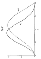
- Figure 2 shows the frequency spectrum of the WAL2 code and that of the code (NC) produced by the code generator according to the invention. The substantial reduction in the high frequency component can be clearly seen from these spectra.
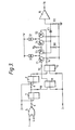
- Figure 3 shows an embodiment of a code generator according to the invention having an input 1 to which a binary code is applied.
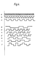
- the binary code applied to terminal 1 is of the form shown in Figure 4d).
- Three clock pulse trains as illustrated in Figure 4a) b) and c) are applied to inputs 2, 3 and 4 respectively.
- Inputs 1 and 4 are connected to respective inputs of an exclusive NOR gate 5 which produces the waveform shown in Figure 4e) on line 6.
- the output of NOR gate 5 is fed via line 6 to the D input of a clocked D type bistable circuit 7 whose clock input is connected to the input 2.
- the Q output of the bistable 7 is connected via a line 8 to the D input of a clocked D type bistable circuit 9 and via a line 10 to the D input of a clocked D type bistable circuit 11.
- the input 2 is connected to the clock input of bistable 9 while the input 3 is connected to the clock input of bistable 11.
- the Q output of bistable 9 is connected to the D input of a clocked D type bistable circuit 12 whose clock input is connected to input 3.
- Bistables 7 and 9 form a two stage shift register with the Q output of bistable 7 providing the waveform 4f) and the Q output of bistable 9 providing waveform 4g).
- waveform 4f) is waveform 4e) delayed by one period of the clock 4a) and waveform 4a) is waveform 4e) delayed by two periods of the clock 4a).
- the Q output of bistable 11 which is shown as waveform 4h) is fed via a line 13 to the base of a ME transistor Tl while the Q output of bistable 12 which is shown as waveform 4i) is fed via a line 14 to the base of a pnp transistor T2.
- the emitter of transistor Tl is connected to the emitter of a pnp transistor T3 and via a constant current source Il to a positive supply rail V.
- the emitter of transistor T2 is connected to the emitter of a pnp transistor T4 and via a constant current source I2 to the positive supply rail V.
- the collectors of transistors Tl and T2 are directly connected to earth while the collectors of transistors T3 and T4 are commoned and connected to earth via a resistor Rl.
- the bases of transistors T3 and T4 are connected to a bias potential VB.
- the collectors of transistors T3 and T4 are additionally connected through a series capacitor Cl to the input of a line driver 15 whose output is connected to the output 16 of the code generator.
- the input of the line driver 15 is connected via a resistor R2 to earth.
- the clock signals applied to inputs 2, 3 and 4 may be generated in known manner by means of an oscillator driving a chain of binary dividers.
- clock signal 4b) is half the frequency of clock signal 4e) while clock signal 4c) is half the frequency of clock signal 4b).
- the period of the clock signal 4c) is equal to the bit period T of the binary signal but is offset with respect to the bit periods by a period T/4.
- the output of bistable 9, waveform 4g) is delayed with respect to the output of bistable 8, waveform 4f), by T/4 i.e. the period of the clock signal 4a).
- the outputs of bistables 8 and 9 are clocked into the bistables 11 and 12 by the clock signal 4c) and as a result the output of bistable 12 on line 14 is an inverted version delayed by T/2 of the output of bistable 11 on line 13.
- the signals on lines 13 and 14 are used to form a three level signal by routing two nominally equal currents I 1 and I 2 into the summing resistor Rl.
- the bistables 11 and 12 are formed as TTL integrated circuits and VB is approximately +1.5 Volts a logic '1' on lines 13 and 14 will cause a current I l + I 2 to flow into resistor Rl, a logic '0' on lines 13 and 14 will prevent any current flowing into resistor Rl, a logic '1' on the line 13 will cause a current of I l to flow into the resistor Rl and a logic '1' on the line 14 will cause a current of I 2 to flow into the resistor Rl.
- the output of amplifier 15 will be of the form shown in Figure 4j).
- the code produced by the code generator replaces the cycle at twice the bit frequency produced in the WAL2 code when the binary signal changes state by a constant level for half the bit period. This has the result of reducing the high frequency content of the transmitted signal while still retaining a second order zero at zero frequency.
- the emitter coupled pair circuits formed by transistors Tl and T3 and transistors T2 and T4 act as first and second switches to switch the currents produced by the first and second current sources I 1 and I 2 into the summing network formed by resistor Rl.
- the switches are controlled by signals on lines 13 and 14 generated by the control circuit comprising the exclusive NOR gate 5 and the D type bistable circuits 7, 9, 11 and 12. It would, of course, be possible to use alternative switching circuits in place of the emitter coupled pair circuits.
Landscapes
- Physics & Mathematics (AREA)
- Spectroscopy & Molecular Physics (AREA)
- Engineering & Computer Science (AREA)
- Computer Networks & Wireless Communication (AREA)
- Signal Processing (AREA)
- Dc Digital Transmission (AREA)
Applications Claiming Priority (2)
| Application Number | Priority Date | Filing Date | Title |
|---|---|---|---|
| GB08132929A GB2109202A (en) | 1981-11-02 | 1981-11-02 | Code generator |
| GB8132929 | 1981-11-02 |
Publications (2)
| Publication Number | Publication Date |
|---|---|
| EP0078577A1 true EP0078577A1 (fr) | 1983-05-11 |
| EP0078577B1 EP0078577B1 (fr) | 1987-01-14 |
Family
ID=10525556
Family Applications (1)
| Application Number | Title | Priority Date | Filing Date |
|---|---|---|---|
| EP82201355A Expired EP0078577B1 (fr) | 1981-11-02 | 1982-10-29 | Générateur de code |
Country Status (7)
| Country | Link |
|---|---|
| US (1) | US4521766A (fr) |
| EP (1) | EP0078577B1 (fr) |
| JP (1) | JPS5885656A (fr) |
| AU (1) | AU557630B2 (fr) |
| CA (1) | CA1215782A (fr) |
| DE (1) | DE3275153D1 (fr) |
| GB (1) | GB2109202A (fr) |
Families Citing this family (3)
| Publication number | Priority date | Publication date | Assignee | Title |
|---|---|---|---|---|
| US4627073A (en) * | 1984-09-28 | 1986-12-02 | Myriad Concepts, Inc. | Binary data transmission method |
| NL8601114A (nl) * | 1986-05-01 | 1987-12-01 | Philips Nv | Transmissiestelsel voor de overdracht van databits. |
| US5461379A (en) * | 1993-12-14 | 1995-10-24 | At&T Ipm Corp. | Digital coding technique which avoids loss of synchronization |
Citations (7)
| Publication number | Priority date | Publication date | Assignee | Title |
|---|---|---|---|---|
| DE2025797A1 (de) * | 1970-05-26 | 1971-12-09 | Siemens Ag | Verfahren und Einrichtung zur Umwandlung eines binären Pulses in einen ternären |
| US3828344A (en) * | 1973-01-02 | 1974-08-06 | Gte Information Syst Inc | Double density to nrz code converter |
| US3993953A (en) * | 1975-10-17 | 1976-11-23 | Gte Automatic Electric Laboratories Incorporated | Apparatus and method for digitally generating a modified duobinary signal |
| DE2529448A1 (de) * | 1975-07-02 | 1977-01-27 | Tekade Felten & Guilleaume | Schaltungsanordnung zur umwandlung von nrz-signalen in rz-signale, insbesondere fuer die synchrone zeitmultiplexbildung |
| DE2744117A1 (de) * | 1977-09-30 | 1979-04-05 | Siemens Ag | Anordnung zum umsetzen dcd-codierter digitaler signale in nrz-signale |
| GB2014401A (en) * | 1978-01-20 | 1979-08-22 | Hitachi Ltd | Data communication system |
| GB1578655A (en) * | 1976-05-15 | 1980-11-05 | Schuetz Udo Kg | Receptacle including an outlet duct for the passage of liquid |
Family Cites Families (3)
| Publication number | Priority date | Publication date | Assignee | Title |
|---|---|---|---|---|
| US2912684A (en) * | 1953-01-23 | 1959-11-10 | Digital Control Systems Inc | Single channel transmission system |
| US2954267A (en) * | 1958-06-05 | 1960-09-27 | Olivetti Corp Of America | Modified return-to-zero digital recording system |
| FR1463043A (fr) * | 1965-09-20 | 1966-06-03 | Trt Telecom Radio Electr | Conditionnement d'informations binaires, en vue de leur transmission |
-
1981
- 1981-11-02 GB GB08132929A patent/GB2109202A/en not_active Withdrawn
-
1982
- 1982-10-25 US US06/436,206 patent/US4521766A/en not_active Expired - Fee Related
- 1982-10-28 CA CA000414418A patent/CA1215782A/fr not_active Expired
- 1982-10-29 DE DE8282201355T patent/DE3275153D1/de not_active Expired
- 1982-10-29 AU AU90012/82A patent/AU557630B2/en not_active Ceased
- 1982-10-29 EP EP82201355A patent/EP0078577B1/fr not_active Expired
- 1982-11-02 JP JP57193269A patent/JPS5885656A/ja active Pending
Patent Citations (7)
| Publication number | Priority date | Publication date | Assignee | Title |
|---|---|---|---|---|
| DE2025797A1 (de) * | 1970-05-26 | 1971-12-09 | Siemens Ag | Verfahren und Einrichtung zur Umwandlung eines binären Pulses in einen ternären |
| US3828344A (en) * | 1973-01-02 | 1974-08-06 | Gte Information Syst Inc | Double density to nrz code converter |
| DE2529448A1 (de) * | 1975-07-02 | 1977-01-27 | Tekade Felten & Guilleaume | Schaltungsanordnung zur umwandlung von nrz-signalen in rz-signale, insbesondere fuer die synchrone zeitmultiplexbildung |
| US3993953A (en) * | 1975-10-17 | 1976-11-23 | Gte Automatic Electric Laboratories Incorporated | Apparatus and method for digitally generating a modified duobinary signal |
| GB1578655A (en) * | 1976-05-15 | 1980-11-05 | Schuetz Udo Kg | Receptacle including an outlet duct for the passage of liquid |
| DE2744117A1 (de) * | 1977-09-30 | 1979-04-05 | Siemens Ag | Anordnung zum umsetzen dcd-codierter digitaler signale in nrz-signale |
| GB2014401A (en) * | 1978-01-20 | 1979-08-22 | Hitachi Ltd | Data communication system |
Also Published As
| Publication number | Publication date |
|---|---|
| DE3275153D1 (en) | 1987-02-19 |
| CA1215782A (fr) | 1986-12-23 |
| AU9001282A (en) | 1983-05-12 |
| JPS5885656A (ja) | 1983-05-23 |
| GB2109202A (en) | 1983-05-25 |
| US4521766A (en) | 1985-06-04 |
| AU557630B2 (en) | 1986-12-24 |
| EP0078577B1 (fr) | 1987-01-14 |
Similar Documents
| Publication | Publication Date | Title |
|---|---|---|
| US5267269A (en) | System and method employing predetermined waveforms for transmit equalization | |
| US5200979A (en) | High speed telecommunication system using a novel line code | |
| US4410878A (en) | Digital signal transmission | |
| WO1985005234A1 (fr) | Emetteur-recepteur a boucle numerique a haute vitesse | |
| CA2138106C (fr) | Emetteur-recepteur de signaux numeriques rapide a technologie cmos | |
| GB2098432A (en) | Consecutive identical digit suppression system | |
| US3986053A (en) | Regenerator for pulse code modulation systems | |
| US7505541B1 (en) | NRZ/PAM-4/PRML triple mode phase and data detector | |
| US6072340A (en) | Pulse shaping and filtering circuit for digital pulse data transmissions | |
| EP0078577B1 (fr) | Générateur de code | |
| JP2000315923A (ja) | バースト光受信回路 | |
| EP1207649A2 (fr) | Communications de données employant des combinaisons de lignes | |
| US4133981A (en) | Time correction circuit for a digital multiplexer | |
| GB2030404A (en) | Pulse shaper for supplying timing pulses to digital circuits | |
| KR100402090B1 (ko) | 신호발생기및전기신호들을발생시키는방법 | |
| US4782484A (en) | Encoding and decoding signals for transmission over a multi-access medium | |
| US6531910B1 (en) | Symmetric multiplexer | |
| US5712875A (en) | Asynchronous differential communication | |
| US5222102A (en) | Digital phased locked loop apparatus for bipolar transmission systems | |
| WO1999022472A1 (fr) | Technique pour coder des trains de donnees numeriques multiples dans une largeur de bande limitee en vue de leur transmission dans un seul support | |
| Neu et al. | Project for a digital telephone network | |
| US6977971B2 (en) | Digital data transmission system with device for correcting baseline wander | |
| RU1837400C (ru) | Кодер позиционного линейного сигнала | |
| JPS6320931A (ja) | デ−タ伝送装置 | |
| KR950000667B1 (ko) | 상호부호간섭과 지터가 없는 대역제한 신호 발생기 |
Legal Events
| Date | Code | Title | Description |
|---|---|---|---|
| PUAI | Public reference made under article 153(3) epc to a published international application that has entered the european phase |
Free format text: ORIGINAL CODE: 0009012 |
|
| 17P | Request for examination filed |
Effective date: 19821029 |
|
| AK | Designated contracting states |
Designated state(s): DE FR GB SE |
|
| GRAA | (expected) grant |
Free format text: ORIGINAL CODE: 0009210 |
|
| AK | Designated contracting states |
Kind code of ref document: B1 Designated state(s): DE FR GB SE |
|
| REF | Corresponds to: |
Ref document number: 3275153 Country of ref document: DE Date of ref document: 19870219 |
|
| ET | Fr: translation filed | ||
| PLBE | No opposition filed within time limit |
Free format text: ORIGINAL CODE: 0009261 |
|
| STAA | Information on the status of an ep patent application or granted ep patent |
Free format text: STATUS: NO OPPOSITION FILED WITHIN TIME LIMIT |
|
| 26N | No opposition filed | ||
| PG25 | Lapsed in a contracting state [announced via postgrant information from national office to epo] |
Ref country code: GB Effective date: 19881029 |
|
| PG25 | Lapsed in a contracting state [announced via postgrant information from national office to epo] |
Ref country code: SE Effective date: 19881030 |
|
| PG25 | Lapsed in a contracting state [announced via postgrant information from national office to epo] |
Ref country code: FR Free format text: LAPSE BECAUSE OF NON-PAYMENT OF DUE FEES Effective date: 19890630 |
|
| PG25 | Lapsed in a contracting state [announced via postgrant information from national office to epo] |
Ref country code: DE Effective date: 19890701 |
|
| GBPC | Gb: european patent ceased through non-payment of renewal fee | ||
| REG | Reference to a national code |
Ref country code: FR Ref legal event code: ST |
|
| EUG | Se: european patent has lapsed |
Ref document number: 82201355.3 Effective date: 19890619 |