EP0078679A2 - Une structure de connexion d'électrodes dans un dispositif semi-conducteur - Google Patents
Une structure de connexion d'électrodes dans un dispositif semi-conducteur Download PDFInfo
- Publication number
- EP0078679A2 EP0078679A2 EP82305765A EP82305765A EP0078679A2 EP 0078679 A2 EP0078679 A2 EP 0078679A2 EP 82305765 A EP82305765 A EP 82305765A EP 82305765 A EP82305765 A EP 82305765A EP 0078679 A2 EP0078679 A2 EP 0078679A2
- Authority
- EP
- European Patent Office
- Prior art keywords
- electrode
- active region
- contact
- semiconductor device
- semiconductor
- Prior art date
- Legal status (The legal status is an assumption and is not a legal conclusion. Google has not performed a legal analysis and makes no representation as to the accuracy of the status listed.)
- Granted
Links
Images


Classifications
-
- H—ELECTRICITY
- H10—SEMICONDUCTOR DEVICES; ELECTRIC SOLID-STATE DEVICES NOT OTHERWISE PROVIDED FOR
- H10D—INORGANIC ELECTRIC SEMICONDUCTOR DEVICES
- H10D30/00—Field-effect transistors [FET]
- H10D30/60—Insulated-gate field-effect transistors [IGFET]
- H10D30/67—Thin-film transistors [TFT]
- H10D30/6729—Thin-film transistors [TFT] characterised by the electrodes
- H10D30/6737—Thin-film transistors [TFT] characterised by the electrodes characterised by the electrode materials
- H10D30/6738—Schottky barrier electrodes
-
- H—ELECTRICITY
- H10—SEMICONDUCTOR DEVICES; ELECTRIC SOLID-STATE DEVICES NOT OTHERWISE PROVIDED FOR
- H10D—INORGANIC ELECTRIC SEMICONDUCTOR DEVICES
- H10D30/00—Field-effect transistors [FET]
- H10D30/60—Insulated-gate field-effect transistors [IGFET]
- H10D30/67—Thin-film transistors [TFT]
- H10D30/674—Thin-film transistors [TFT] characterised by the active materials
- H10D30/675—Group III-V materials, Group II-VI materials, Group IV-VI materials, selenium or tellurium
-
- H—ELECTRICITY
- H10—SEMICONDUCTOR DEVICES; ELECTRIC SOLID-STATE DEVICES NOT OTHERWISE PROVIDED FOR
- H10D—INORGANIC ELECTRIC SEMICONDUCTOR DEVICES
- H10D30/00—Field-effect transistors [FET]
- H10D30/80—FETs having rectifying junction gate electrodes
-
- H—ELECTRICITY
- H10—SEMICONDUCTOR DEVICES; ELECTRIC SOLID-STATE DEVICES NOT OTHERWISE PROVIDED FOR
- H10D—INORGANIC ELECTRIC SEMICONDUCTOR DEVICES
- H10D62/00—Semiconductor bodies, or regions thereof, of devices having potential barriers
- H10D62/80—Semiconductor bodies, or regions thereof, of devices having potential barriers characterised by the materials
- H10D62/85—Semiconductor bodies, or regions thereof, of devices having potential barriers characterised by the materials being Group III-V materials, e.g. GaAs
-
- H—ELECTRICITY
- H10—SEMICONDUCTOR DEVICES; ELECTRIC SOLID-STATE DEVICES NOT OTHERWISE PROVIDED FOR
- H10D—INORGANIC ELECTRIC SEMICONDUCTOR DEVICES
- H10D64/00—Electrodes of devices having potential barriers
- H10D64/60—Electrodes characterised by their materials
- H10D64/62—Electrodes ohmically coupled to a semiconductor
-
- H—ELECTRICITY
- H10—SEMICONDUCTOR DEVICES; ELECTRIC SOLID-STATE DEVICES NOT OTHERWISE PROVIDED FOR
- H10D—INORGANIC ELECTRIC SEMICONDUCTOR DEVICES
- H10D64/00—Electrodes of devices having potential barriers
- H10D64/60—Electrodes characterised by their materials
- H10D64/64—Electrodes comprising a Schottky barrier to a semiconductor
-
- H—ELECTRICITY
- H10—SEMICONDUCTOR DEVICES; ELECTRIC SOLID-STATE DEVICES NOT OTHERWISE PROVIDED FOR
- H10W—GENERIC PACKAGES, INTERCONNECTIONS, CONNECTORS OR OTHER CONSTRUCTIONAL DETAILS OF DEVICES COVERED BY CLASS H10
- H10W20/00—Interconnections in chips, wafers or substrates
- H10W20/40—Interconnections external to wafers or substrates, e.g. back-end-of-line [BEOL] metallisations or vias connecting to gate electrodes
Definitions
- the present invention relates to a semiconductor device, more particularly, an electrode connection structure in a semiconductor integrated circuit device.
- a semiconductor integrated circuit device in particular, one comprising a compound semiconductor such as gallium arsenide (GaAs), gallium arsenide/gallium aluminum arsenide (GaAs/GaAlAs), or indium phosphide (InP), often includes two or more types of electrodes of different materials interconnected with each other.
- a metal semiconductor field effect transister (MES FET) using GaAs has gate electrodes of, e.g., aluminum (Al), which makes Schottky contact with GaAs of an active region, and source and drain electrodes of, e.g., gold-germanium (AuGe), which makes ohmic contact with GaAs of the active region.
- MES FET metal semiconductor field effect transister
- a GaAs integrated circuit (IC) which is' integrated with such MES FET's requires electrical connections between the above two types of electrodes.
- Figures 1 to 3 show an inverter circuit as an example of such connections.
- Figure 1 is a circuit diagram of an inverter circuit
- Fig. 2 a plan view of the patterns for elements of the inverter circuit of Fig. 1, and Fig. 3 a sectional view taken on the line III-III in Fig. 2.
- a driver transistor Tr l a load transistor Tr 2 , and a next stage driver transistor Tr 3 are MES FET's.
- the gate of the load transistor Tr 2 is connected to the source of the load transistor Tr 2 as well as the drain of the driver transistor Tr l and the gate of the next stage driver transistor Tr 3 .
- the gate of the driver transistor Tr 1 is an inlet terminal (IN).
- the drain of the load transistor Tr 2 is connected to one side of a power source (V DD ).
- the source of the driver transistor Tr 1 is connected to the other side of the power source or the ground (V SS ).
- active regions 2a and 2b exist as an N-type or N +- type region on which gate electrodes 3a, 3b, and 3c and drain or source electrodes 4a, 4b, and 4c are formed, the metal of the gate electrodes 3a, 3b, and 3c and the metal of the drain or source electrodes 4a, 4b, and 4c being different and making Schottky contact and ohmic contact, respectively with GaAs. All the electrodes 3a, 3b, 3c, 4a, 4b, and 4c are covered with a silicon dioxide (Si0 2 ) layer 5 (not shown in Fig. 2).
- Si0 2 silicon dioxide
- interconnecting lines 6a and 6b made of, e.g., titanium-platinum--gold (TiPtAu) are formed, extending from the electrodes 4a and 4b through contact windows 7a and 7b, respectively.
- the Tr 2 gate electrode 3b, Tr 2 source and Tr 1 drain electrode 4c, and Tr 3 gate electrode 3c are connected by means of connecting portions 8a and 8b.
- Three through holes 7c, 9a, and 9b are opened in the SiO 2 layer 5 above the connecting portions 8a and 8b and the electrode 4c.
- These connecting portions 8a and 8b and the electrode 4c are connected by interconnecting lines 6c, 10a, and 10b made of TiPtAu.
- the reason for connecting the gate electrode 3b and the drain or source electrode 4c by means of the interconnecting lines 6c 10a, and 10b is that if the aluminum (Al) of the gate electrode and the gold-germanium (AuGe) of the drain or source electrode are directly connected with each other, the aluminum and the gold would react with each other to form purple plaque, an intermetallic compound, lowering the yield and reliability of the semiconductor device.
- the gate electrodes 3b, 3c and the drain or source electrode 4c are connected by means of the interconnecting lines 6c, 10a, and 10b, by way of respective through holes 7c, 9a, and 9b. Such connections may easily result in insufficient electrical contact between the interconnecting lines and the electrodes due to presence of Si0 2 residue in the through holes.
- connections made by means of through holes 9a and 9b require increased area for formation, since consideration must be given to tolerances in aligning the through holes 9a, 9b with the connecting portions 8a and 8b of the gate electrodes 3b and 3c respectively and in aligning the interconnecting lines 10a and 10b with the through holes 9a and 9b respectively.
- This increased area for through hole connections lowers the degree of integration of a semiconductor integrated circuit device having the above described inverter circuit.
- the through holes 9a and 9b are formed in a square of 2 /um (microns) x 2 /um and the connecting portions 8a and 8b of the gate electrodes 3b and 3c are formed in a square of 6 /um x 6 /um.
- the interconnecting lines 10a and 10b are formed so as to include a square of 4 /um x 4 /um near the position of the through holes 9a, 9b. Further, there is a distance of about 2pm between the connecting portions 8a and 8b of the gate electrodes 3b and 3c and the active region 2a and between the connecting portions 8a and 8b and the active region 2b. Therefore, 10 /um distance is needed between the active regions 2a and 2b.
- titanium-platinum-gold can be considered in place of aluminum as the gate-electrode metal so as to avoid the formation of the above-mentioned purple plaque and to avoid the increased area of connection portions by means of interconnecting lines and through holes.
- the titanium-platinum-gold line as an extending portion of gate electrodes can directly ride on the source or drain electrode and make contact between them without the formation of purple plaque, an intermetallic compound between aluminum and gold.
- the direct connection between the two types of electrodes of different metals enables elimination of the use of the interconnecting lines as well as the connection by means of through holes between the interconnecting lines and the electrodes, and, therefore, the decrease of the size necessary for making the connections between the two types of electrodes, that is, the elimination of the tolerances in alignment of layers at the through holes.
- a titanium-platinum-gold electrode which makes Schottky: contact with gallium arsenide cannot be formed before ohmic contact is formed since the heat treatment necessary for making the ohmic contact has an adverse effect on the Schottky- contact. Therefore, the titanium-platinum--gold line as mentioned above can ride on the source or drain electrode only within the boundaries of the source or drain electrode, an ohmic contact-making electrode. This reduces the reliability of the contact between them and lowers the yield of the semiconductor device due to possible disconnection at the step appearing at the edge of the source or drain electrode.
- titanium-platinum--gold (TiPtAu) gate electrode does not allow source and drain regions to be made using the gate electrode as a mask for ion implantation or diffusion since the gate electrode cannot be made before the ohmic contact-making source and drain electrodes.
- This requires tolerances in alignment of the gate electrode with the source and drain regions, increasing the distance between the source and drain regions. This requirement also appears in the case of, e.g., aluminum gate electrode (see. Naoki Yokoyama's Japanese Patent Application No. 55-189544 filed on December 30, 1980; U.S. Patent Application Serial No. 334923 filed on December 28, 1981; and European Patent Application No. 81306151.2 filed on December 24, 1981).
- a semiconductor device comprises a semiconductor layer defining an active region and is characterised by: a first part of an electrode on the active region and of a material selected from the group of high melting point metals and silicide of high melting point metals and making Schottky contact with the active region; and a second part of the electrode, on the active region, in contact with the first part of the electrode, and of a material different from the material of the first part of the electrode and making ohmic contact with the active region.
- High melting point metals which make Schottky contact with a semiconductor active region or layer include .titanium. tungsten (TiW); and silicides of high melting point metals which make Schottky contact with' a semiconductor active region or layer include titanium tungsten silicide (TiWSi) and tungsten silicide (WSi).
- TiW titanium tungsten silicide
- WSi tungsten silicide
- the Schottky contact made between one of these metals and a semiconductor is not adversely affected by the heat treatment for making ohmic contact, e.g. a temperature of 400°C to 450°C. This feature makes it possible to use more types of electrode structures than in the prior art.
- a semiconductor device comprises a semiconductor layer defining an active region and a first electrode on a first active region, making Schottky contact with the first active region and is characterised by: a first part of a second electrode on a second active region and extendingfrom the first electrode with the same material as that of said first electrode; and, a second part of the second electrode on the second active region, in contact with said first part of the second electrode, and of material different from that of the first electrode and making ohmic contact with the second active region.
- FIGS. 4 and 5 show an example of an inverter circuit embodying the present invention and similar in basic configuration to the inverter circuit of Figs. 1 to 3.
- gate electrodes 13a, 13b, and 13c are made of titanium tung- stenide silicide (TiWSi) which makes Schottoky contact with GaAs of a substrate 11.
- TiWSi titanium tung- stenide silicide
- the gate electrodes 13b and 13c are formed without disconnection between them by extending the gate electrodes 13b and 13c on the surfaces of active regions lla and 12a, respectively, to the surface of the semi-insulating substrate.
- the extending and connecting portion 21 of the gate electrodes 13b and 13c has a branch line 22 extending to a Tr l -drain-electrode- and Tr 2 -source- electrode- forming portion on the surface of the active region 12a.
- the gate electrodes 13a, 13b, and 13c and their extending portions 21 and 22 can be formed in one step by a lithographic technique. Further, the extending portion 22 of the gate electrode 13b and 13c on the active region 12a is covered with a gold-germanium (AuGe) alloy layer 23, the alloy of which makes ohmic contact with GaAs of the active region 12a.
- AuGe gold-germanium
- the AuGe layer 23 on the surface of the active region 12a surrounds the extending portion 22 and makes ohmic contact with the active region 12a at three sides of the extending portion 22 of the gate electrode 13b and 13c.
- the action of the Schottky contact of the extending portion 22 does not affect the action of the AuGe layer 23 (and therefore the action of the inverter circuit), if the AuGe layer 23 straddles the extending portion 22 of the gate electrode 13b and 13c in the drain-to-source direction and makes ohmic contact with the active region 12a there.
- the extending portion 22 of the gate electrodes 13b and 13c and the AuGe layer 23 covering the extending portion 22 form an electrode 24 which serves as the source electrode of Tr 1 and the drain electrode of Tr 2 .
- the drain region of Tr I and the source region of Tr 2 are connected to the gates 13b and 13c of Tr 2 and Tr 3 through the AuGe layer 23 and the extending portions 22 and 21.
- the AuGe layer 23 can be formed simultaneously in the step for forming the electrodes 14a and 14b.
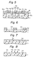
- FIG. 6 to 12 illustrate the steps of fabricating the inverter circuit of Fig. 4 and 5.
- the semi-insulating substrate 11 is a chromium (Cr) doped or undoped GaAs substrate having a resistivity of 10 6 to 10 S ohm-cm.
- a silicon dioxide (Si0 2 ) layer 31 and a photoresist layer 32 are formed and selectively patterned so as to implant silicon (Si) ions into the substrate 11 by using the patterned layers 31 and 32 as a mask.
- Dosages of 1 x 10 12 cm -2 and 2 x 10 12 cm -2 and an implantation energy of 59 keV are used for making a region 33 for a enhancement-type channel of Tr 1 and a region 34 for an depletion-type channel of Tr 2 , respectively (Fig. 6).
- the depth of the implantations is about 1000A, but the region 34 is slightly deeper in depth and slightly higher in impurity concentration than the region 33 due to the difference of their dosages.
- the silicon (Si) ion implanted regions 33 and 34 are annealed at 850°C for 10 to 15 minutes in an atmosphere of nitrogen (N 2 ) + 10% hydrogen (H 2 ) (Fig. 7).
- an approximately 4500 to 5000A-thick TiWSi layer is deposited on the substrate 1 by sputtering and is selectively dry etched so as to form gate electrodes 13a, 13b and 13c and their extending portions 21 and 22 (3c and 21 are not shown in Fig. 7), the width of the gate electrodes and the extending portion being about I /um (Fig. 8).
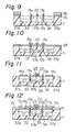
- silicon ions are implanted in a dosage of 1.7 x 10 13 cm -2 and at an implantation energy of 175 keV to form active layers (i.e., a source region 37a, a drain region 37b of Tr l , a source region 37c, and a drain region 37d of Tr 2 ) by using,as masks for ion implantation,patterned SiO 2 and photoresist layers 35 and 36 as well as the gate electrodes 3a and 3b and the extending portion 22 in the opening of the patterned Iayers 35 and 36 (Fig. 9).
- active layers i.e., a source region 37a, a drain region 37b of Tr l , a source region 37c, and a drain region 37d of Tr 2
- the ion implanted regions are annealed at 800°C for 5 to 10 minutes in an atmosphere of nitrogen (N 2 ) + 10% hydrogen (H 2 ) using a cover of a SiO 2 layer 38, resulting in a depth of the active layers 37a, 37b, 37c, 37d of about 3000A (Fig. 10).
- ohmic contact elec- trodesl4a,14c, and 23 are formed by depositing an approxi- mately 300 to 350A-thick AuGe layer and then an approxi- mately 3000A-thick gold layer on given portions by using a lift-off technique and annealing them at 450°C for 1 minute to make an alloy of the AuGe of the electrodes 14a, 14c and 22 and the GaAs of substrate (Fig. 11).
- the electrodes 13a, 13b, 14a, 14c, and 23 and the substrate 1 are covered with a SiO 2 layer 15 having a thickness of about 5000A, in which through holes 17a andl7c are opened to lead out interconnecting lines 16 made of a 500A-thick titanium (Ti) layer and a 7000A-thick gold layer thereon (Fig. 12 and Fig. 5).
- the width of the electrode 24 (the size in the right-to-left direction in Fig. 4) can be about 4 /um instead of about 6 ,um, as in the prior art example.
- the distance between the active regions 12a and 12b can be about 6 /um since 2 /um distances are needed between the extending portion 21 of the gate electrodes 13b and 13c and the active regions 12a and 12b and a 2 /um width is needed for the extending portion 21, including the tolerances in alignment.
- the distance between the source region 37a or 37c and the drain region 37b or 37d, respectively can be the same as the width of the gate electrode 13a or 13b itself, respectively, due to the self- alignment of the source and drain regions with the gate electrode by use of the gate electrode as a mask for forming the source and drain regions by ion implantation or diffusion, resulting in a decrease of that distance, i.e., the length of the gate.
- the semiconductor integrated circuit device having, e.g., the above described inverter circuit can be densified so as to improve the degree of integration of the device.
Landscapes
- Junction Field-Effect Transistors (AREA)
- Electrodes Of Semiconductors (AREA)
Applications Claiming Priority (2)
| Application Number | Priority Date | Filing Date | Title |
|---|---|---|---|
| JP56174038A JPS5874084A (ja) | 1981-10-29 | 1981-10-29 | 半導体装置 |
| JP174038/81 | 1981-10-29 |
Publications (3)
| Publication Number | Publication Date |
|---|---|
| EP0078679A2 true EP0078679A2 (fr) | 1983-05-11 |
| EP0078679A3 EP0078679A3 (en) | 1985-05-22 |
| EP0078679B1 EP0078679B1 (fr) | 1987-12-23 |
Family
ID=15971535
Family Applications (1)
| Application Number | Title | Priority Date | Filing Date |
|---|---|---|---|
| EP82305765A Expired EP0078679B1 (fr) | 1981-10-29 | 1982-10-29 | Une structure de connexion d'électrodes dans un dispositif semi-conducteur |
Country Status (4)
| Country | Link |
|---|---|
| US (1) | US4628338A (fr) |
| EP (1) | EP0078679B1 (fr) |
| JP (1) | JPS5874084A (fr) |
| DE (1) | DE3277892D1 (fr) |
Cited By (3)
| Publication number | Priority date | Publication date | Assignee | Title |
|---|---|---|---|---|
| US4745445A (en) * | 1983-03-15 | 1988-05-17 | Itt Gallium Arsenide Technology Center, A Division Of Itt Corporation | Interdigitated Schottky diode |
| EP0283278A3 (en) * | 1987-03-18 | 1989-09-06 | Fujitsu Limited | Compound semiconductor device having nonalloyed ohmic contacts |
| KR100778258B1 (ko) * | 1999-11-15 | 2007-11-22 | 램 리써치 코포레이션 | 플라스마의 용적을 제어하는 방법 및 장치 |
Families Citing this family (11)
| Publication number | Priority date | Publication date | Assignee | Title |
|---|---|---|---|---|
| JP2577719B2 (ja) * | 1984-07-06 | 1997-02-05 | テキサス インスツルメンツ インコ−ポレイテツド | 電界効果トランジスタのソース電極構造 |
| FR2603146B1 (fr) * | 1986-08-19 | 1988-11-10 | Thomson Csf | Source de courant de type charge active et son procede de realisation |
| US4947220A (en) * | 1987-08-27 | 1990-08-07 | Yoder Max N | Yoked, orthogonally distributed equal reactance amplifier |
| US5254483A (en) * | 1987-10-23 | 1993-10-19 | Vitesse Semiconductor Corporation | Gate-to-ohmic metal contact scheme for III-V devices |
| US5121174A (en) * | 1987-10-23 | 1992-06-09 | Vitesse Semiconductor Corporation | Gate-to-ohmic metal contact scheme for III-V devices |
| JPH01161773A (ja) * | 1987-12-18 | 1989-06-26 | Agency Of Ind Science & Technol | 化合物半導体装置の製造方法 |
| JPH02271537A (ja) * | 1989-04-12 | 1990-11-06 | Mitsubishi Electric Corp | 半導体装置及びその製造方法 |
| US5388577A (en) * | 1990-06-08 | 1995-02-14 | Boston University | Electrode array microchip |
| DE4113969A1 (de) * | 1991-04-29 | 1992-11-05 | Telefunken Electronic Gmbh | Verfahren zur herstellung von ohmschen kontakten fuer verbindungshalbleiter |
| KR102423194B1 (ko) * | 2015-01-21 | 2022-07-21 | 삼성디스플레이 주식회사 | 유기 발광 표시 장치 및 그 유기 발광 표시 장치의 접속패드 검사방법 |
| JP2018148012A (ja) * | 2017-03-06 | 2018-09-20 | サンケン電気株式会社 | 半導体装置 |
Family Cites Families (8)
| Publication number | Priority date | Publication date | Assignee | Title |
|---|---|---|---|---|
| US3877051A (en) * | 1972-10-18 | 1975-04-08 | Ibm | Multilayer insulation integrated circuit structure |
| FR2210725B1 (fr) * | 1972-12-15 | 1976-08-27 | Leduc Gerard | |
| US4048646A (en) * | 1975-02-26 | 1977-09-13 | Nippon Electric Company, Limited | Dual-gate schottky barrier gate fet having an intermediate electrode and a method of making same |
| US4186410A (en) * | 1978-06-27 | 1980-01-29 | Bell Telephone Laboratories, Incorporated | Nonalloyed ohmic contacts to n-type Group III(a)-V(a) semiconductors |
| US4263605A (en) * | 1979-01-04 | 1981-04-21 | The United States Of America As Represented By The Secretary Of The Navy | Ion-implanted, improved ohmic contacts for GaAs semiconductor devices |
| JPS55125666A (en) * | 1979-03-23 | 1980-09-27 | Nec Corp | Semiconductor device |
| US4300149A (en) * | 1979-09-04 | 1981-11-10 | International Business Machines Corporation | Gold-tantalum-titanium/tungsten alloy contact for semiconductor devices and having a gold/tantalum intermetallic barrier region intermediate the gold and alloy elements |
| DE3005733A1 (de) * | 1980-02-15 | 1981-08-20 | Siemens AG, 1000 Berlin und 8000 München | Verfahren zur herstellung einer halbleiteranordnung und nach diesem verfahren hergestellte halbleiteranordnung |
-
1981
- 1981-10-29 JP JP56174038A patent/JPS5874084A/ja active Granted
-
1982
- 1982-10-29 DE DE8282305765T patent/DE3277892D1/de not_active Expired
- 1982-10-29 EP EP82305765A patent/EP0078679B1/fr not_active Expired
-
1985
- 1985-09-25 US US06/779,618 patent/US4628338A/en not_active Expired - Fee Related
Cited By (4)
| Publication number | Priority date | Publication date | Assignee | Title |
|---|---|---|---|---|
| US4745445A (en) * | 1983-03-15 | 1988-05-17 | Itt Gallium Arsenide Technology Center, A Division Of Itt Corporation | Interdigitated Schottky diode |
| EP0283278A3 (en) * | 1987-03-18 | 1989-09-06 | Fujitsu Limited | Compound semiconductor device having nonalloyed ohmic contacts |
| US4961194A (en) * | 1987-03-18 | 1990-10-02 | Fujitsu Limited | Compound semiconductor device having nonalloyed ohmic contacts |
| KR100778258B1 (ko) * | 1999-11-15 | 2007-11-22 | 램 리써치 코포레이션 | 플라스마의 용적을 제어하는 방법 및 장치 |
Also Published As
| Publication number | Publication date |
|---|---|
| JPH0324061B2 (fr) | 1991-04-02 |
| US4628338A (en) | 1986-12-09 |
| JPS5874084A (ja) | 1983-05-04 |
| EP0078679A3 (en) | 1985-05-22 |
| DE3277892D1 (en) | 1988-02-04 |
| EP0078679B1 (fr) | 1987-12-23 |
Similar Documents
| Publication | Publication Date | Title |
|---|---|---|
| EP0078679A2 (fr) | Une structure de connexion d'électrodes dans un dispositif semi-conducteur | |
| EP0206274B1 (fr) | Structure IC complémentaire à haute transconductance | |
| EP0725432B1 (fr) | Transistor à effet de champ à hétérostructure et à porte réfractaire et méthode | |
| EP0188879A2 (fr) | TEC à canal de bord | |
| US4701996A (en) | Method for fabricating edge channel FET | |
| KR100349953B1 (ko) | 밀리미터파 대역에서 안정적으로 동작 가능한 전계 효과 트랜지스터 및 그 제조 방법 | |
| US5770489A (en) | Method of making a compound semiconductor field-effect transistor | |
| US4904613A (en) | Method of manufacturing a DMOS device | |
| US4771324A (en) | Heterojunction field effect device having an implanted region within a device channel | |
| JPH0156534B2 (fr) | ||
| US4335502A (en) | Method for manufacturing metal-oxide silicon devices | |
| EP0687016B1 (fr) | Transistor à effet de champ à jonction et procédé de fabrication | |
| CA1271850A (fr) | Methode de fabrication de transistors a effet de champ a grille a auto-alignement | |
| US4929568A (en) | Method of isolating a top gate of a MESFET and the resulting device | |
| JPH04280436A (ja) | 相補型自己整合hfetの製造方法 | |
| JPS5934666A (ja) | 半導体集積回路装置 | |
| EP0297508A2 (fr) | Dispositif semi-conducteur complémentaire à structure hétérogène | |
| KR980012637A (ko) | 반도체 장치 및 그 제조방법 | |
| JPS62177920A (ja) | 半導体装置の製造方法 | |
| JPS60225468A (ja) | 電界効果型半導体装置およびその製造方法 | |
| JP2000100935A5 (fr) | ||
| JPS5866363A (ja) | 電界効果トランジスタの製造方法 | |
| JPS61125087A (ja) | 絶縁ゲ−ト型電界効果半導体装置及びその製造方法 | |
| JPS61134069A (ja) | 半導体装置およびその製造方法 | |
| JPS6265377A (ja) | 半導体装置およびその製造方法 |
Legal Events
| Date | Code | Title | Description |
|---|---|---|---|
| PUAI | Public reference made under article 153(3) epc to a published international application that has entered the european phase |
Free format text: ORIGINAL CODE: 0009012 |
|
| AK | Designated contracting states |
Designated state(s): DE FR GB |
|
| PUAL | Search report despatched |
Free format text: ORIGINAL CODE: 0009013 |
|
| AK | Designated contracting states |
Designated state(s): DE FR GB |
|
| 17P | Request for examination filed |
Effective date: 19851111 |
|
| 17Q | First examination report despatched |
Effective date: 19860605 |
|
| GRAA | (expected) grant |
Free format text: ORIGINAL CODE: 0009210 |
|
| AK | Designated contracting states |
Kind code of ref document: B1 Designated state(s): DE FR GB |
|
| ET | Fr: translation filed | ||
| REF | Corresponds to: |
Ref document number: 3277892 Country of ref document: DE Date of ref document: 19880204 |
|
| PLBE | No opposition filed within time limit |
Free format text: ORIGINAL CODE: 0009261 |
|
| STAA | Information on the status of an ep patent application or granted ep patent |
Free format text: STATUS: NO OPPOSITION FILED WITHIN TIME LIMIT |
|
| 26N | No opposition filed | ||
| PGFP | Annual fee paid to national office [announced via postgrant information from national office to epo] |
Ref country code: FR Payment date: 19971009 Year of fee payment: 16 |
|
| PGFP | Annual fee paid to national office [announced via postgrant information from national office to epo] |
Ref country code: GB Payment date: 19971020 Year of fee payment: 16 |
|
| PGFP | Annual fee paid to national office [announced via postgrant information from national office to epo] |
Ref country code: DE Payment date: 19971110 Year of fee payment: 16 |
|
| PG25 | Lapsed in a contracting state [announced via postgrant information from national office to epo] |
Ref country code: GB Free format text: LAPSE BECAUSE OF NON-PAYMENT OF DUE FEES Effective date: 19981029 |
|
| GBPC | Gb: european patent ceased through non-payment of renewal fee |
Effective date: 19981029 |
|
| PG25 | Lapsed in a contracting state [announced via postgrant information from national office to epo] |
Ref country code: FR Free format text: LAPSE BECAUSE OF NON-PAYMENT OF DUE FEES Effective date: 19990630 |
|
| REG | Reference to a national code |
Ref country code: FR Ref legal event code: ST |
|
| PG25 | Lapsed in a contracting state [announced via postgrant information from national office to epo] |
Ref country code: DE Free format text: LAPSE BECAUSE OF NON-PAYMENT OF DUE FEES Effective date: 19990803 |