EP0079410A1 - Raumthermostateinrichtung mit Tageszeitprogrammgeber - Google Patents
Raumthermostateinrichtung mit Tageszeitprogrammgeber Download PDFInfo
- Publication number
- EP0079410A1 EP0079410A1 EP81401787A EP81401787A EP0079410A1 EP 0079410 A1 EP0079410 A1 EP 0079410A1 EP 81401787 A EP81401787 A EP 81401787A EP 81401787 A EP81401787 A EP 81401787A EP 0079410 A1 EP0079410 A1 EP 0079410A1
- Authority
- EP
- European Patent Office
- Prior art keywords
- output
- circuit
- terminal
- contact
- digital
- Prior art date
- Legal status (The legal status is an assumption and is not a legal conclusion. Google has not performed a legal analysis and makes no representation as to the accuracy of the status listed.)
- Granted
Links
Images



Classifications
-
- G—PHYSICS
- G04—HOROLOGY
- G04G—ELECTRONIC TIME-PIECES
- G04G15/00—Time-pieces comprising means to be operated at preselected times or after preselected time intervals
- G04G15/006—Time-pieces comprising means to be operated at preselected times or after preselected time intervals for operating at a number of different times
-
- G—PHYSICS
- G05—CONTROLLING; REGULATING
- G05D—SYSTEMS FOR CONTROLLING OR REGULATING NON-ELECTRIC VARIABLES
- G05D23/00—Control of temperature
- G05D23/19—Control of temperature characterised by the use of electric means
- G05D23/1902—Control of temperature characterised by the use of electric means characterised by the use of a variable reference value
- G05D23/1904—Control of temperature characterised by the use of electric means characterised by the use of a variable reference value variable in time
-
- G—PHYSICS
- G05—CONTROLLING; REGULATING
- G05D—SYSTEMS FOR CONTROLLING OR REGULATING NON-ELECTRIC VARIABLES
- G05D23/00—Control of temperature
- G05D23/19—Control of temperature characterised by the use of electric means
- G05D23/20—Control of temperature characterised by the use of electric means with sensing elements having variation of electric or magnetic properties with change of temperature
- G05D23/24—Control of temperature characterised by the use of electric means with sensing elements having variation of electric or magnetic properties with change of temperature the sensing element having a resistance varying with temperature, e.g. a thermistor
Definitions
- the present invention relates to a room thermostat device with daily programmer, comprising a thermostat, a digital clock, a program selection circuit, a set point switching circuit and a circuit for controlling the switching circuit controlled by the digital output of the digital clock and through the program selection circuit.
- patent FR 2 449 922 there is described a device with room thermostats combined with a time switch, in which a day thermostat is connected in series with a night thermostat and in which the day thermostat can be short- operated by a contact controlled by a clock motor.
- a battery is provided which is permanently charged by a rectifier circuit supplied by the mains.
- the use of a battery has intrinsic drawbacks and the cost of a rectifier circuit as well as the expense of charging current are significant.
- the installation of a clock motor with the means, not described, for controlling the short-circuit contact leads to considerable bulk.
- the mains must be connected.
- a device for periodic and programmed switching of intervals for raising and lowering the temperature in premises.
- the device comprises at least two thermostats which are switched by the output of a comparator, one input of which is connected to the output of a current time memory and two other inputs are respectively connected to the outputs of two programmable switching time memories.
- the means used in this device ie digital memories and digital comparator, are relatively expensive.
- the device can only program one start time for comfort temperature and one start time for lowered temperature.
- the digital clock is no longer powered.
- a third wire is provided for the operation of the clock.
- thermostats are particularly easy to use for the user and that their size is reduced.
- One object of the invention is to provide a device with a room thermostat allowing two set temperatures, one called comfort and the other called economy or lowering which can be predetermined according to now, if such a provi- does not also require that two son for connection to the device for controlling the heat source, which is simple to use and whose size is of the order of the simple thermostats mentioned above.
- the device must be able to be used in premises with various vocations, which implies that it must allow the choice between several possible programs going for example up to including up to three daily periods at comfort temperature separated by three periods at lowering temperature.
- Another object of the invention consists in providing a device with an ambient thermostat with a daily programmer controlled by a clock supplied by an electric current source constituted by electric batteries.
- electric batteries which is spreading more and more, imposes only one condition, that is to say that the consumption of the circuits supplied by the batteries is very low so as to space out their replacements as well as possible.
- digital display clocks powered by simple batteries is also becoming more and more common.
- the control circuit comprises a digital / decimal converter converting the digital data from time units to one of ten, ten codes outputs of the converter being connected to the vertical wires of a matrix of crossing points with three pairs of output wires, the output pairs being respectively assigned to the hours whose tens digits are 2, 1 and 0, which are connected to the inputs correspondents of a logic circuit further comprising inputs connected to the outputs of the active clock when the ten hour digit is 1 or 2, respectively, points of crossover of the matrix being selectively connected according to the various scheduled operating programs , electronic contacts being mounted on the output wires of the matrix and controlled by the program selection circuit, the output of the logic circuit being re linked to the setpoint adjustment potentiometer, the voltage transmitted to said potentiometer by the logic circuit output varying between two values according to the logic states of the inputs of the logic circuit.
- the program selection circuit has outputs directly connected to said logic circuit to force the potential of the output of said logic circuit to one value or another, whatever the time.
- the thermostat comprises a bistable relay, means for supplying the coil of the bistable relay in one direction or the other during the successive changes of states of the output of the temperature detector of the thermostat, a contact of said relay bistable closing or opening the thermostat output circuit, and means for cutting the power supply to the coil between changes of state of the output of said temperature detector.
- the output of said temperature detector in the high state for a heat demand and in the low state in the opposite case, is connected to the first two inputs of a first and of a second door.
- NAND directly and through an inverter, the second inputs of the first and second NAND doors being respectively connected to the fixed working contact and the fixed resting contact of a second coil contact whose movable contact is at '' low state, the outputs of the first and second NAND gates being respectively connected to the control inputs of a first and of a second electronic contact, the first electronic contact being mounted between the positive terminal of a first battery and the first terminal of the coil whose second terminal is connected to the negative terminal of the first battery and the second electronic contact being mounted between the negative terminal of a second battery and the first terminal of the coil whose second terminal is rel connected to the positive terminal of the second battery, the first contact SW.2 being open in the rest position.
- a delay circuit is provided between the second input of the first NAND gate and the corresponding fixed contact of the second contact.
- the digital clock is powered by the battery source.
- an inverter between the output terminal rear panel of the clock and the corresponding input terminal of the display is mounted an inverter, the other input terminal of which is connected to the flashing output of the digital circuit of the clock, the inverter being controlled by a circuit for measuring the voltage across the battery source which switches the blink output terminal to the signal input on the rear panel of the display when said voltage drops below a predetermined threshold.
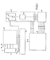
- the device according to the invention comprises a thermostat 10, a source of electric batteries 11, a control circuit 12, capable of actuating the control member of the heat (or cold) source, not shown , a digital clock 13, a programming coding matrix 14 and a control circuit for switching 15.
- the direct current electrical source 11 consists of three batteries SI, S2 and S3, connected in series and of an f.e.m. 1.5 V each.
- the positive terminal of the battery SI is connected to the + terminal of the source while the negative terminal of the battery S3 is connected by a resistance RI of 1 kilohm to the - terminal of the source.
- a capacitor C1 of 22 microfarads.
- the positive and negative terminals of the battery S2 are respectively connected, by two resistors R2 and R3 of 1 kilohm each, to two wires V + and V-, between which is mounted a capacitor C2 of 2.2 microfarad.
- Between the V + wire and the + terminal is also mounted a C3 capacitor of 2.2 microfarads.
- Thermostat 10 conventionally comprises a bridge, one branch of which is constituted by a resistor R4 and a thermistor Th and the other branch of which is constituted by three resistors R5, R6 and R7 in series, the resistor R6 being mounted in parallel with a potentiometer Pl
- the common terminal at R4 and R5 is connected to wire V + while the common terminal at Th and R7 is connected to wire V-.
- the terminal common to R4 and Th is connected to terminal "2" of a differential amplifier Amp while the cursor of potentiometer Pl is connected to terminal "3" thereof.
- the amplifier Amp is, for example, of the LM 4250CN type, with its terminal "7" connected to the terminal +, its terminal "4" to the terminal - and its terminal "8" to the terminal - by a resistor R8 of 2.2 megohms.
- the output "6" of the amplifier Amp is connected, by a resistor R9 of 470 kilohms and a capacitor C4 of 2.2 microfarads, to the terminal -. Resistor R9 and capacitor C4 constitute a delay circuit.
- the terminal common to R9 and C4 is connected to the input of an inverter INV1, operating as a trigger of the MC 14093BCP type, the output of which is connected, on the one hand, to the input "2" of the amplifier Amp , by a resistance R10 of 22 megohms, to form a reaction circuit which defines the hysteresis of the thermostat, and, on the other hand, to a wire F1 whose high state defines the state of heat demand and the low state the state of cessation of heat demand.
- R6 and R7 The point common to R6 and R7 is still connected by a resistor R11 at the cursor of a potentiometer P2, one terminal of which is connected to the - terminal of the source 11 and the other terminal to a wire F2.
- the wire F1 is connected, on the one hand, to the input of a logic inverter INV2 and, on the other hand, to an input of a NAND gate Gl, the other of which input is connected, on the one hand, to terminal + of 11 by a resistor R12 of 2.2 megohms and, on the other hand, to the working contact of a change-over contact SW.1.
- the output of the inverter INV2 is connected to an input of a NAND gate G2 the other input of which is connected, on the one hand, to the terminal + of 11 by a resistance R13 of 2.2 megaohms and, on the other hand, in the rest contact of contact SW.1.
- the movable contact of SW.1 is connected to the - terminal of the source 11.
- the contact SW.1 is the contact of a bistable electromagnetic relay, of the EBERLE type 408-21-024, whose coil SW is mounted between the terminal common to S2 and S3, on the one hand, and the point common to both collectors of two transistors TR1 and TR2, on the other hand.
- the output of the NAND gate G1 is connected by a resistor R14 of 10 kilohms to the base of a PNP transistor TR3 while the output of the NAND gate G2 is connected by a resistor R15 of 10 kilohms to the base of a PNP TR4 transistor.
- the emitter of transistor TR3 is connected, on the one hand, to the base of the PNP transistor TRI and, on the other hand, to terminal + by a resistor R16 of 10 kilohms.
- the collector of transistor TR3 is connected to the negative terminal of S3 by a resistor R17 of 160 ohms.
- the emitter of transistor TR4 is directly connected to the + terminal while its collector is connected to the negative terminal of S3 by two resistors R18 of 160 ohms and R19 of 10 kilohms in series.
- the point common to R18 and R19 is connected to the base of the NPN transistor TR2.
- the transmitter of TRI is connected to the terminal + while that of TR2 is connected to the negative terminal of S3.
- a diode Dl Between terminal + and the point common to the collectors of TR1 and TR2 is mounted a diode Dl while between this same common point and the negative terminal of S3 is mounted a diode D2.
- the relay SW has a second working contact SW.2 which, in the working position, connects two wires F3 and F4 and, in the rest position, disconnects them.
- the wires F3 and F4 are connected to the control element of the heat source, not shown, and play exactly the same role as the output wires of a simple thermostat.
- the relay SW In the position shown in FIG. 2, the relay SW is at rest, the contact SW.2 is open, which means that there is no heating demand, and the contact SW.1 connects the terminal - to an input of door G2 , i.e. applies a low state to this input.
- the output of the inverter INV1 is also in the low state. It follows that the outputs of the gates GI and G2 can activate neither the transistor TR3, nor the transistor TR4, and, consequently, neither the transistor TRI, nor the transistor TR2. These last two transistors being blocked, no current flows through the coil SW at rest.
- SW.2 closes the circuit of F3 and F4 which triggers the heat source and SW.1 brings an input of Gl to the low state, which blocks the transistors TR3 and TRI, and an input of G2 to the high state, the other input of G2 being kept low by the output of INV2 whose input is high, which keeps the transistors TR2 and TR4 blocked.
- the voltage at the terminals of the batteries drops, but without disturbing the operation of the other electronic circuits, for which the supply voltage is maintained by the capacitor C1.
- the diodes Dl and D2 are provided to suppress the counter-electromotive force currents induced by the coil SW.
- the wire F2 is at the terminal's potential - during comfort periods and at a more positive potential than the terminal - during lowering periods.
- the point common to R6 and R7 is more negative in times of comfort than in times of decline. Therefore, the output of the differential amplifier Amp changes state, for a heat demand, at a higher temperature in comfort period than in lowering period.
- the potentiometer Pl makes it possible to adjust the comfort temperature and the potentiometer P2 makes it possible to adjust the lowering of the temperature for the periods of economy.
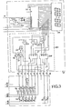
- the digital clock 13 is a commercial clock which, in the example described, consists of an integrated circuit Zl and a display device DA where the hours and minutes are displayed in conventional seven-segment code.
- the integrated circuit Zl of the ICM 7223 type marketed by Intersil, is controlled by a quartz crystal QZ with conventional mounting connected to its terminals "33" and "34", and is supplied by its terminal "32" connected to the terminal +, its terminal "31” connected to wire V + and its terminal "26” connected to terminal -.
- a conventional RH time reset circuit is connected to terminals "36" and "37" of Zl.
- Terminals "2" to "8" of circuit Zl used to display the hour unit digit, are connected to the inputs of a digital / decimal D / D converter which includes three NAND gates G3 to G5 of the type MC 14023BCP, three gates OU-NON G6 to G8 of type MC 14001BCP and two logic circuits G9 and G10 of type MC 14555BCP.
- Terminal "2" of Zl is connected to an input of G5 and an input of G6.
- Terminal "3" of Zl is connected to an input of G5 and an input of G9.
- Terminal "4" of Z1 is connected to an input of G10.
- Terminal "5" of Zl is connected to the third input of G5.
- the output "6" of Z1 is connected to an input of G3 and an input of G4.
- the output "7” of Z1 is connected to an input of G10 while the output "8" is connected to an input of G9.
- the output of G5 is connected to the third input of G10 and, in parallel, to two inputs of G4.
- the output of G4 is connected to the third entry of G9.
- Two inputs of G3 are connected to the terminal + and its output is connected to the input E2 of the matrix 14.
- the circuit G9 has four outputs, the first connected to the input E3 of 14, the second to the inputs of G8, the third at input E4 and the fourth at input El of 14.
- the circuit G10 has four outputs, the first connected to input E8, the second to input E9, the third to input E6 and the fourth at entry E5 from 14.
- the exit from gate G8 is connected to an entry from G6 and G7.
- the output of gate G6 is connected to an input of gate G7 and the input E7 of 14.
- the output of G7 is connected to input EO of 14.
- the terminals of circuits G9 and G10 carry the numerical references from the manufacturer.
- the D / D converter converts the binary information delivered by ZI on its seven terminals "2" to "8" into one of ten code on the inputs EO to E9 of the matrix 14.
- Each activated EO to E9 input indicates the 'hour unit 0 to 9 displayed by DA.
- the structure of the D / D converter is given by way of example, but it is obvious that it can be produced with components other than those which are shown. This is why we will not describe in detail the operation of N / D.
- the programming matrix 14 comprises three pairs of output wires 00, not used, and 01 to 05. If we consider that vertical wires starting from inputs EO to E9 and horizontal wires starting from outputs 01 to 05, we obtain a matrix of crossing points, the wires of which can be identified by their respective points of origin.
- diodes D3 At the intersection of E3 and 01 is mounted diodes D3; diodes D4 to D7 are mounted at the crossing points of E0, E3, E4, and E5, on the one hand, and of 02, on the other hand; diodes D8 and D9 are mounted at the crossing points of El and E2 on the one hand and of 03 on the other hand; diodes D10 to D15 are mounted at the crossing points of EO to E5, on the one hand, and 04, on the other hand; and at the crossing points of E8 and E9, on the one hand, and 05, on the other hand, are mounted diodes D16 and D17. All these diodes are mounted in the direct direction between the inputs and outputs of the matrix 14.
- the switching control circuit 15, FIG. 4 includes a switching logic circuit Z2 which, in the example described, is of the MC 14053BCP type, and a program selector SP, as well as a number of components that we will see below.
- circuit Z2 terminals "1” to “6” and “9” to “ 15” are used.
- the circuit Z2 comprises three pairs of electronic contacts X1, X2; X3, X4; and X5, X6, each pair forming an inverter.
- Contact Xl connects terminals "5" and “4" when terminal “9” of Z2 is low, while contact X2 connects terminals "3" and "4", when terminal “9” is high.
- Contact X3 connects terminals "4" and “15”, by “2", when terminal "10” is in the low state, while contact X4 connects terminals "1” and "15” when terminal "10” is high.
- the output "38" of Z1 delivers the state of the "rear panel BP" of the display device DA.
- the circuit ICM 7223 constituting the circuit Z1 delivers to each segment of the display device DA an alternating signal at 32 Hz in phase or in opposition phase with the rear panel output according to the activated or inactive state of the segment.
- the signals applied by the circuit Zl to the D / D converter are alternating signals at 32 Hz so that the signals delivered to the terminals "1", “3” and "5" of Z2 by the D / D converter, through the matrix 14, are valid only during the low state of the output "38" of Z2.
- the circuit formed by X6 of Z2, R21, X10 and C5 allows the previous state of terminal "13” of Z2 to be memorized during the high state of output "38" of Zl. Indeed, if the previous state of terminals "13” and “14", was low, the control input of X10 is low and X10 is open so that the potential of the terminal - is applied to "13” through R22, 14 and X6. previous state of terminals "13” and "14" was high, contact X10 is closed, thus applying the potential of terminal + to terminal "13".
- the program selector SP includes five pads PR1 to PR5 which can be individually set to the potential of terminal + by actuating it.
- the pad PR1 is connected to terminal "6" of Z2 and the pad PR5 is connected to the control input of X10.
- PR2 is isolated
- PR3 is connected, by a diode D18, respectively to the control inputs of the electronic contacts X7 and X9
- the pad PR4 is connected, by a diode D19, respectively to the control inputs of the electronic contacts X7 and X9, and is connected directly to the control input of the electronic contact X8.
- the control inputs of contacts X7 to X9 are connected to the terminal - by load resistors R23 to R25.
- terminal "13" of circuit Z2 is connected to the output wire F2 and therefore constitutes the output signal terminal.
- terminal "13" and wire F2 are isolated, while in lowering mode, they are at the positive potential of terminal +. So, in the first case, the cursor of P2, Fig. 2, is at the terminal potential - while in the other, there is an intermediate potential between + and - which defines the temperature difference.
- the configuration of the diode array 14 has been given by way of example, although it makes it possible to satisfy the most common needs of users, it is possible to provide other configurations making it possible to satisfy users having other constraints. It will also be understood that the diodes D3 to D19 are only examples of crossing points among others. Likewise, the structure of the logic circuit of FIG. 4 could be changed.
- Fig. 6 shows a variant of the circuit 12, as regards an input circuit of the door G1, FIG. 2.
- a resistor R26 is mounted in this variant between contact SW.1 and the input of G1.
- this input of G1 is connected to terminal + by a capacitor C6.
- Resistor R26 and capacitor C6 form a delay circuit which ensures an offset between the change of state of the contact SW.l and that which results therefrom for the gate Gl, there is therefore a slight offset in time. In practice, this offset makes it possible to ensure that the door Gl does not change state before the magnetic circuit of the relay SW is completely closed.
- a variant of the D / D converter has been shown, there are the doors G3 to G5 and the circuits G9 and GIO, but all the doors G6 to G8 have been replaced by a circuit Z3 which, in the example described, is of the MC 14053BCP type, like Z2.
- the circuit Z3 is used in a circuit for controlling the voltage of the batteries of the source 11.
- Circuit Z3 includes three pairs of electronic contacts X11 to X16. Contact X11 is closed when terminal “9” is high and contact X12 is closed otherwise. Contact X13 is closed when terminal “10” is high, contact X14 not used in the example described. Contact X15 is closed when terminal “11” is high and contact X16 is closed otherwise. Furthermore, circuit Z3 has its terminal “15” connected to terminal +, its terminals “1” and “2” connected together, its terminal “9” connected to the output “2” of circuit Zl, its terminal “10 “connected to the second output of circuit G9, its terminal” 5 “connected to the input EO of the matrix 14 and its output” 3 "connected to the input E7 of the matrix 14.
- Terminal “11” is connected to the collector of a PNP transistor TR5, the emitter of which is connected to terminal + and the base at an intermediate point of a voltage divider formed, between terminals + and -, of the resistance R27 of 560 kilohms, of potentiometer P3 of 47 kilohms and resistance R28 of 62 kilohms, the intermediate point being the point common to R27 and P3.
- the collector of TR5 is connected to terminal + by a resistance R29 of 1 megohm.
- the potentiometer slider allows you to precisely adjust the voltage of the base of TR5 in relation to the voltage of its transmitter.
- Terminal "12" of Z3 is connected to output "38" (rear panel) of Zl, this output no longer being connected directly to terminal "40" of the display DA, as in FIG. 3.
- the terminal "13" of Z3 is connected to the output "9” of the circuit Zl, which is connected to the display DA to ensure the flashing at 1 Hz of the light points separating the hours from the minutes.
- Terminal "14" of Z3 is connected to terminal "40" of DA.
- FIGs in Figs. 5a to 5e illustrate, depending on the time, the comfort or lowering states for the five programs PR5, PR1, PR2, PR4 and PR3, respectively.
- FIG. 9 shows that the device hooks onto a base 20 fixed on a partition and connected to the heat source by the wires F3 and F4.
- the device has two plugs 21 and 22 which are inserted from bottom to high in the contacts of a female socket 23 connected to the wires F3 and F4.
- a screw 24, carried by a bracket 25 is provided for screwing into a tapped hole 26 of the housing of the device.
- the battery compartment S1 to S3 can be closed by a sliding plate 27 on which the program diagrams of Figs are engraved or inscribed.
- an SP button which can be operated vertically, allows you to select a program
- a P1 button which can be operated vertically, allows you to choose the comfort temperature.
- a window 28 makes it possible to read the time on the display and, at the bottom, two windows 29 and 30 make it possible to read the comfort temperature chosen and the program chosen.
- the potentiometer P2 is controlled by a wheel which is preferably located at the hidden rear of the housing to avoid any untimely operation and thus ensure a suitable temperature difference between the comfort temperature and the lowering temperature.
- Buttons 31 on the side of the device allow setting the clock time.
Landscapes
- Physics & Mathematics (AREA)
- General Physics & Mathematics (AREA)
- Engineering & Computer Science (AREA)
- Automation & Control Theory (AREA)
- Control Of Temperature (AREA)
- Electric Clocks (AREA)
- Control Of Indicators Other Than Cathode Ray Tubes (AREA)
- Electronic Switches (AREA)
Priority Applications (5)
| Application Number | Priority Date | Filing Date | Title |
|---|---|---|---|
| DE8181401787T DE3176096D1 (en) | 1981-11-12 | 1981-11-12 | Room thermostat device with a day-time programmer |
| AT81401787T ATE26497T1 (de) | 1981-11-12 | 1981-11-12 | Raumthermostateinrichtung mit tageszeitprogrammgeber. |
| EP81401787A EP0079410B1 (de) | 1981-11-12 | 1981-11-12 | Raumthermostateinrichtung mit Tageszeitprogrammgeber |
| CA000414626A CA1191580A (en) | 1981-11-12 | 1982-11-01 | Daily programmable thermostat assembly |
| US06/439,111 US4428528A (en) | 1981-11-12 | 1982-11-04 | Environmental thermostat assembly |
Applications Claiming Priority (1)
| Application Number | Priority Date | Filing Date | Title |
|---|---|---|---|
| EP81401787A EP0079410B1 (de) | 1981-11-12 | 1981-11-12 | Raumthermostateinrichtung mit Tageszeitprogrammgeber |
Publications (2)
| Publication Number | Publication Date |
|---|---|
| EP0079410A1 true EP0079410A1 (de) | 1983-05-25 |
| EP0079410B1 EP0079410B1 (de) | 1987-04-08 |
Family
ID=8188564
Family Applications (1)
| Application Number | Title | Priority Date | Filing Date |
|---|---|---|---|
| EP81401787A Expired EP0079410B1 (de) | 1981-11-12 | 1981-11-12 | Raumthermostateinrichtung mit Tageszeitprogrammgeber |
Country Status (5)
| Country | Link |
|---|---|
| US (1) | US4428528A (de) |
| EP (1) | EP0079410B1 (de) |
| AT (1) | ATE26497T1 (de) |
| CA (1) | CA1191580A (de) |
| DE (1) | DE3176096D1 (de) |
Cited By (2)
| Publication number | Priority date | Publication date | Assignee | Title |
|---|---|---|---|---|
| FR2593276A1 (fr) * | 1986-01-21 | 1987-07-24 | Mumbach Pierre | Systeme de programmation et de controle automatique de la temperature interieure de locaux individuels tels que par exemple des appartements |
| EP2273679A1 (de) | 2009-07-07 | 2011-01-12 | Somfy SAS | Heimsender vom Typ Steuerpunkt und vom Sensortyp für die kapazitive Erkennung |
Families Citing this family (16)
| Publication number | Priority date | Publication date | Assignee | Title |
|---|---|---|---|---|
| US4551009A (en) * | 1981-12-21 | 1985-11-05 | Mita Industrial Co., Ltd. | Electrostatic copying apparatus |
| CA1171938A (fr) | 1983-01-07 | 1984-07-31 | David Bensoussan | Controleur automatique de temperature, de chauffage d'air conditionne et d'humidite sensible au mouvement et a la lumiere |
| US4506827A (en) * | 1983-10-17 | 1985-03-26 | Johnson Service Company | Battery powered thermostat |
| JPS61167827A (ja) * | 1985-01-21 | 1986-07-29 | Omron Tateisi Electronics Co | 電子温度計 |
| US4751961A (en) * | 1986-02-18 | 1988-06-21 | Honeywell Inc. | Electronic programmable thermostat |
| US4688547A (en) * | 1986-07-25 | 1987-08-25 | Carrier Corporation | Method for providing variable output gas-fired furnace with a constant temperature rise and efficiency |
| US4799176A (en) * | 1986-12-29 | 1989-01-17 | Harper-Wyman Company | Electronic digital thermostat |
| US5361215A (en) | 1987-05-27 | 1994-11-01 | Siege Industries, Inc. | Spa control system |
| US6965815B1 (en) | 1987-05-27 | 2005-11-15 | Bilboa Instruments, Inc. | Spa control system |
| USD326234S (en) | 1988-12-19 | 1992-05-19 | Graesslin Kg | Combined thermostat and timer |
| US5329991A (en) * | 1992-11-05 | 1994-07-19 | Hunter Fan Company | Pre-programmed electronic programmable thermostat |
| US5251813A (en) * | 1993-03-25 | 1993-10-12 | Emerson Electric Co. | Indication of low battery voltage condition by altering of temperature setpoint |
| USD364824S (en) | 1994-06-27 | 1995-12-05 | Carrier Corporation | Thermostat |
| US5982987A (en) * | 1997-04-30 | 1999-11-09 | Mcdonald; Donald E. | Solid state thermostat |
| US20070045442A1 (en) * | 2005-08-31 | 2007-03-01 | Ranco Incorporated Of Delaware | Thermostat display system providing backlight warning |
| US9285134B2 (en) * | 2007-12-14 | 2016-03-15 | Honeywell International Inc. | Configurable wall module system |
Citations (7)
| Publication number | Priority date | Publication date | Assignee | Title |
|---|---|---|---|---|
| US3931550A (en) * | 1974-11-25 | 1976-01-06 | The United States Of America As Represented By The Secretary Of The Navy | Electronic latching relay control |
| US4049193A (en) * | 1975-08-04 | 1977-09-20 | Fuel Computer Corporation | Systems and apparatus for control of fueled heat generators |
| FR2385135A1 (fr) * | 1977-03-25 | 1978-10-20 | Radiotechnique Compelec | Programmateur journalier, notamment pour economie d'energie par modulation de chauffage |
| FR2429810A1 (fr) * | 1978-06-26 | 1980-01-25 | Toray Silicone Co | Compositions pour la fabrication de pellicules decollables |
| US4191328A (en) * | 1977-09-01 | 1980-03-04 | Rapidcircuit Corp. | Integral thermostat-digital clock unit |
| FR2449922A1 (fr) * | 1978-11-29 | 1980-09-19 | Vedette Fabrique Horlogerie | Thermostat d'ambiance combine a un interrupteur horaire a reserve de marche |
| US4235368A (en) * | 1979-08-27 | 1980-11-25 | Teledyne Industries, Inc. | Thermostat assembly |
Family Cites Families (3)
| Publication number | Priority date | Publication date | Assignee | Title |
|---|---|---|---|---|
| FR2446509A1 (fr) | 1977-04-29 | 1980-08-08 | Garret Roger | Programmateur |
| US4154397A (en) | 1978-02-08 | 1979-05-15 | International Telephone And Telegraph Corporation | Night set-back thermostat |
| US4277784A (en) | 1979-07-13 | 1981-07-07 | Commodore Electronics Limited | Switch scanning means for use with integrated circuits |
-
1981
- 1981-11-12 DE DE8181401787T patent/DE3176096D1/de not_active Expired
- 1981-11-12 EP EP81401787A patent/EP0079410B1/de not_active Expired
- 1981-11-12 AT AT81401787T patent/ATE26497T1/de not_active IP Right Cessation
-
1982
- 1982-11-01 CA CA000414626A patent/CA1191580A/en not_active Expired
- 1982-11-04 US US06/439,111 patent/US4428528A/en not_active Expired - Fee Related
Patent Citations (7)
| Publication number | Priority date | Publication date | Assignee | Title |
|---|---|---|---|---|
| US3931550A (en) * | 1974-11-25 | 1976-01-06 | The United States Of America As Represented By The Secretary Of The Navy | Electronic latching relay control |
| US4049193A (en) * | 1975-08-04 | 1977-09-20 | Fuel Computer Corporation | Systems and apparatus for control of fueled heat generators |
| FR2385135A1 (fr) * | 1977-03-25 | 1978-10-20 | Radiotechnique Compelec | Programmateur journalier, notamment pour economie d'energie par modulation de chauffage |
| US4191328A (en) * | 1977-09-01 | 1980-03-04 | Rapidcircuit Corp. | Integral thermostat-digital clock unit |
| FR2429810A1 (fr) * | 1978-06-26 | 1980-01-25 | Toray Silicone Co | Compositions pour la fabrication de pellicules decollables |
| FR2449922A1 (fr) * | 1978-11-29 | 1980-09-19 | Vedette Fabrique Horlogerie | Thermostat d'ambiance combine a un interrupteur horaire a reserve de marche |
| US4235368A (en) * | 1979-08-27 | 1980-11-25 | Teledyne Industries, Inc. | Thermostat assembly |
Cited By (3)
| Publication number | Priority date | Publication date | Assignee | Title |
|---|---|---|---|---|
| FR2593276A1 (fr) * | 1986-01-21 | 1987-07-24 | Mumbach Pierre | Systeme de programmation et de controle automatique de la temperature interieure de locaux individuels tels que par exemple des appartements |
| EP2273679A1 (de) | 2009-07-07 | 2011-01-12 | Somfy SAS | Heimsender vom Typ Steuerpunkt und vom Sensortyp für die kapazitive Erkennung |
| FR2947975A1 (fr) * | 2009-07-07 | 2011-01-14 | Somfy Sas | Emetteur domotique de type point de commande et de type sensitif a detection capacitive. |
Also Published As
| Publication number | Publication date |
|---|---|
| US4428528A (en) | 1984-01-31 |
| EP0079410B1 (de) | 1987-04-08 |
| CA1191580A (en) | 1985-08-06 |
| ATE26497T1 (de) | 1987-04-15 |
| DE3176096D1 (en) | 1987-05-14 |
Similar Documents
| Publication | Publication Date | Title |
|---|---|---|
| EP0079410B1 (de) | Raumthermostateinrichtung mit Tageszeitprogrammgeber | |
| EP0208597A1 (de) | Leistungsanpassungsgerät für elektrische Anlage, insbesondere häusliche Anlage | |
| GB2181833A (en) | Computing device for suntanning dose measurement, and process for producing optical filters | |
| US4902906A (en) | Security lighting system | |
| FR2482739A1 (fr) | Montre electronique | |
| EP0037315A1 (de) | Steuerungsanordnung der Helligkeitsänderungen einer Lichtanlage im Laufe der Zeit | |
| EP0911851B1 (de) | Vorrichtung zur Steuerung eines Schutzschalters | |
| FR2461972A1 (fr) | Interrupteur horaire a reserve de marche et a microcalculateur ou microprocesseur | |
| EP0787994B1 (de) | Stromzähler | |
| FR2719440A1 (fr) | Appareil de contrôle d'une installation électrique d'une habitation particulière. | |
| EP0321626A1 (de) | Durch einen Elektromotor angetriebener Riegel sowie elektronische Sicherheitssteuerung | |
| EP0176383A1 (de) | Verfahren zur programmierten Zeitschaltung | |
| BE1014621A3 (fr) | Procede pour l'adaptation de la periode de prelevement d'energie electrique sur le reseau de distribution par des appareils electriques pour le rechauffement a accumulation, en particulier des chauffe-eau, et dispositif electronique pour l'application du dit procede. | |
| FR2586833A1 (fr) | Interrupteur horaire a programmation fixe et commandable | |
| FR3131963A3 (fr) | Ensemble domotique et de contrôle intégral compact et à haut rendement pour véhicules récréatifs | |
| FR2477282A1 (fr) | Dispositif de controle de la capacite de batteries d'accumulateurs | |
| FR2472786A1 (fr) | Procede et dispositif de conduite de processus physique | |
| EP0229540A1 (de) | Elektronischer Thermostat | |
| CN215869274U (zh) | 一种记忆开关元件 | |
| FR2563348A1 (fr) | Installations decentralisees de programmation et de regulation de grandeur physique, notamment de temperature | |
| EP0034971A1 (de) | Fernprogrammiervorrichtung für eine Zentralheizungsanlage | |
| KR950013669B1 (ko) | 마이크로 컴퓨터를 이용한 자동 점멸기 및 그 제어방법 | |
| FR2583178A1 (fr) | Circuit de controle de la duree de blocage d'un appareil a duree de blocage programmable, notamment pour coffre-fort | |
| BE1015718A3 (fr) | Dispositif electronique pour l'application d'un procede pour l'adaptation de la periode de prelevement d'energie electrique sur le reseau. | |
| FR2636142A1 (fr) | Compteur d'electricite a deux ou plusieurs tarifs de comptage |
Legal Events
| Date | Code | Title | Description |
|---|---|---|---|
| PUAI | Public reference made under article 153(3) epc to a published international application that has entered the european phase |
Free format text: ORIGINAL CODE: 0009012 |
|
| AK | Designated contracting states |
Designated state(s): AT BE CH DE FR GB IT LI LU NL SE |
|
| 17P | Request for examination filed |
Effective date: 19831229 |
|
| GRAA | (expected) grant |
Free format text: ORIGINAL CODE: 0009210 |
|
| AK | Designated contracting states |
Kind code of ref document: B1 Designated state(s): AT BE CH DE FR GB IT LI LU NL SE |
|
| PG25 | Lapsed in a contracting state [announced via postgrant information from national office to epo] |
Ref country code: NL Effective date: 19870408 Ref country code: IT Free format text: LAPSE BECAUSE OF FAILURE TO SUBMIT A TRANSLATION OF THE DESCRIPTION OR TO PAY THE FEE WITHIN THE PRESCRIBED TIME-LIMIT;WARNING: LAPSES OF ITALIAN PATENTS WITH EFFECTIVE DATE BEFORE 2007 MAY HAVE OCCURRED AT ANY TIME BEFORE 2007. THE CORRECT EFFECTIVE DATE MAY BE DIFFERENT FROM THE ONE RECORDED. Effective date: 19870408 Ref country code: AT Effective date: 19870408 |
|
| REF | Corresponds to: |
Ref document number: 26497 Country of ref document: AT Date of ref document: 19870415 Kind code of ref document: T |
|
| PG25 | Lapsed in a contracting state [announced via postgrant information from national office to epo] |
Ref country code: SE Effective date: 19870430 |
|
| REF | Corresponds to: |
Ref document number: 3176096 Country of ref document: DE Date of ref document: 19870514 |
|
| NLV1 | Nl: lapsed or annulled due to failure to fulfill the requirements of art. 29p and 29m of the patents act | ||
| PG25 | Lapsed in a contracting state [announced via postgrant information from national office to epo] |
Ref country code: LU Free format text: LAPSE BECAUSE OF NON-PAYMENT OF DUE FEES Effective date: 19871130 Ref country code: LI Effective date: 19871130 Ref country code: CH Effective date: 19871130 Ref country code: BE Effective date: 19871130 |
|
| PLBE | No opposition filed within time limit |
Free format text: ORIGINAL CODE: 0009261 |
|
| STAA | Information on the status of an ep patent application or granted ep patent |
Free format text: STATUS: NO OPPOSITION FILED WITHIN TIME LIMIT |
|
| 26N | No opposition filed | ||
| BERE | Be: lapsed |
Owner name: SOC. DELTA DORE S.A. Effective date: 19871130 |
|
| GBPC | Gb: european patent ceased through non-payment of renewal fee | ||
| REG | Reference to a national code |
Ref country code: CH Ref legal event code: PL |
|
| PG25 | Lapsed in a contracting state [announced via postgrant information from national office to epo] |
Ref country code: DE Effective date: 19880802 |
|
| PG25 | Lapsed in a contracting state [announced via postgrant information from national office to epo] |
Ref country code: GB Effective date: 19881121 |
|
| PGFP | Annual fee paid to national office [announced via postgrant information from national office to epo] |
Ref country code: FR Payment date: 19951130 Year of fee payment: 15 |
|
| PG25 | Lapsed in a contracting state [announced via postgrant information from national office to epo] |
Ref country code: FR Effective date: 19970731 |
|
| REG | Reference to a national code |
Ref country code: FR Ref legal event code: ST |