EP0079698B1 - Système de traitement de données avec un dispositif pour la commande d'interruptions de programme - Google Patents
Système de traitement de données avec un dispositif pour la commande d'interruptions de programme Download PDFInfo
- Publication number
- EP0079698B1 EP0079698B1 EP82305668A EP82305668A EP0079698B1 EP 0079698 B1 EP0079698 B1 EP 0079698B1 EP 82305668 A EP82305668 A EP 82305668A EP 82305668 A EP82305668 A EP 82305668A EP 0079698 B1 EP0079698 B1 EP 0079698B1
- Authority
- EP
- European Patent Office
- Prior art keywords
- interrupt
- interrupts
- level
- priority
- vectored
- Prior art date
- Legal status (The legal status is an assumption and is not a legal conclusion. Google has not performed a legal analysis and makes no representation as to the accuracy of the status listed.)
- Expired
Links
Images



Classifications
-
- G—PHYSICS
- G06—COMPUTING OR CALCULATING; COUNTING
- G06F—ELECTRIC DIGITAL DATA PROCESSING
- G06F9/00—Arrangements for program control, e.g. control units
- G06F9/06—Arrangements for program control, e.g. control units using stored programs, i.e. using an internal store of processing equipment to receive or retain programs
- G06F9/46—Multiprogramming arrangements
- G06F9/48—Program initiating; Program switching, e.g. by interrupt
- G06F9/4806—Task transfer initiation or dispatching
- G06F9/4812—Task transfer initiation or dispatching by interrupt, e.g. masked
-
- G—PHYSICS
- G06—COMPUTING OR CALCULATING; COUNTING
- G06F—ELECTRIC DIGITAL DATA PROCESSING
- G06F13/00—Interconnection of, or transfer of information or other signals between, memories, input/output devices or central processing units
- G06F13/14—Handling requests for interconnection or transfer
- G06F13/20—Handling requests for interconnection or transfer for access to input/output bus
- G06F13/32—Handling requests for interconnection or transfer for access to input/output bus using combination of interrupt and burst mode transfer
- G06F13/34—Handling requests for interconnection or transfer for access to input/output bus using combination of interrupt and burst mode transfer with priority control
Definitions
- the present invention relates to a data processing system having an apparatus for controlling interruptions in the program, wherein a series of input-output (I/O) units is connected by means of a system bus to a central unit, each I/O unit including an interrupt circuit for generating a corresponding vectored interrupt for the central processing unit and the I/O units being interconnected by daisy chain means, the processing unit being capable of accepting non-vectored interrupts generated by the operating system in consequence of predetermined operations and having lower priority level than the vectored interrupts, the said apparatus being adapted to mask interrupts of a lower priority in response to an interrupt of a higher priority level.
- I/O input-output
- vectored interrupts are capable of masking non-vectored interrupts, which are of lower priority than the vectored interrupts.
- such a system is unable to resolve the conflicts which derive from simultaneous requests for a plurality of interrupts of the same category.
- peripheral devices To share one level among many peripheral devices and to solve the problem of contention between them, these devices are connected in a daisy chain. If a chain is rather long, the connection is rather unreliable and the masking of the interrupt of lower priority in the same level is relatively slow.
- Patents Abstracts of Japan, Volume 6, No. 5, 13 January 1982, P-97 (883) discloses a series of I/O units divided in two levels, the units of each level being connected in two corresponding daisy chains, which are connected to a switching circuit. This arrangement is however unable to connect the two chains to act as a single chain, the two ends of which are directly connected to the interrupt control unit.
- the object of the present invention is to provide an apparatus for controlling with simple and reliable operations the vectored interrupts by arranging them in a plurality of levels of priorities.
- the data processing system has a mono-processor structure, in which a central processing unit CPU (Fig. 1) provides for internal computing and control of a series of operating stations and peripheral devices by way of a single bus 21 of master/slave type, with which the various units are interfaced.
- the bus 21 may comprise up to fourteen interfaces, to each of which the CPU is serially connected, the CPU always performing the function of master, that is to say, having the capacity to acquire control of the bus for handling transfer operations.
- a RAM memory for example an 8M byte memory
- I/O input-output
- the units will always include a control unit KB/D for an alpha-numeric keyboard 23 and a video CRT, for example a 15" CRT for around 2000 characters, a control unit FDU for a floppy magnetic disc drive, 24 and a control unit PRU for a serial printer 26.
- the bus 21 may also have connected thereto a control unit HDU for a high-capacity hard magnetic disc drive 27 and a control unit STC for a device 28 for reading and writing a magnetic tape cassette.
- Other control units may also be connected to the bus 21, as generally indicated at 29, for optional devices such as badge reading and/or recording devices, numeric keyboards for use by the customer, known as PIN-pad, means for reading and/or marking documents with magnetic characters, banknote dispenser means, and the like.
- the bus 21 may also have connected thereto other slave control units SCU for operating stations with a keyboard, video means and printer.
- SCU slave control units
- the bus 21 may also have connected thereto other slave control units SCU for operating stations with a keyboard, video means and printer.
- other slave control units SCU for operating stations with a keyboard, video means and printer.
- the central unit essentially comprises a 16 bit microprocessor pP, a unit MMU for controlling the RAM and a specific logic unit LU.
- the microprocessor and the unit MMU are known per se and are not part of the present invention.
- the specific logic unit LU will be described in greater detail hereinafter.
- microprocessor and the MMU comprise two integrated circuits marketed by the company Zilog, which will only be described briefly herein, while reference may be made to the description published by the above-mentioned company for further details of the circuits.
- the microprocessor comprises a control unit 33 (Fig. 2) which receives the instructions supplied by an instruction register 34 and decoded by an instruction decoder 35. That in turn is connected to an arithmetic and logic unit ALU 36 and a group of 16 bit working registers RP ... R15 which in turn are connected to the ALU 36.
- the group of registers RO... R15 may generally perform the functions of accumulators, index registers routine or program address stacks and memory pointers.
- the registers RO ... R15 however may be organised for selectively processing 8 bit bytes, 16 bit words, double 32 bit words and quadruple 64 bit words.
- the microprocessor also includes a 16 bit interface register 40 for data and addresses.
- the control unit 33 despatches the various orders to the exterior by way of a series of connections 38 which include four connections STa-ST3 for controlling the state of the microprocessor; two connections BRQ and BAK for controlling the bus 21 and other connections for timing signals, power supply, etc.
- Another group of connections generally indicated by reference numeral 39 is provided for the transfer of data and address of the register 40 and segment addresses SNa-SN7 which will be referred to hereinafter.
- the MMU controls the RAM, essentially performing two functions: the conversion of a logic memory address into a physical address and protection of the memory sector in accordance with attribute or qualification.
- the RAM may be subdivided into a number of regions or segments up to 128 and each segment may have a length of a number of blocks of 256 bytes, variable from 1 to 256, -whereby the length of the segment may be up to 64 K bytes.
- Each byte of the RAM is addressed with a logic address formed by the original number of the segment and the ordinal number of the byte in that segment, which will be referred to hereinafter as the offset.
- the number of the segment is indicated by seven bits, while the offset requires sixteen bits, of which eight of higher significance represent the blocks.
- Each memory segment may be attributed with a given limit for the field and for a given function, for example for preventing writing (Read-Only), or preventing access to the microprocessor or reserving it for the operative system, etc.
- the MMU comprises a group of registers 41 describing the memory segments. Each register is formed by two words and upon initialisation is set up with the physical address of the respective segment and the relevant limit and function attributes or qualifications.
- the registers 41 are addressed by the 7 bits of the number of the segment, from the channel SNa-SN6 of the group 39. Those bits provide at the output of the registers 41, the physical address of the origin of the segment.
- That output is added in an adder 42 with the eight more significant bits of the offset, from another channel A/D8-A/D15 of the group 39.
- the physical address of the RAM is provided by the output of a third channel A/DO-A/D7 of the group 39 and the sixteen bits A8-A23 outputted by the adding means 42.
- the MMU further includes a logic circuit 43 capable of controlling each request for access to an address in the memory, with the qualifications or attributes for the respective memory segment, provided by the registers 41, and responds to any violations by creating an internal interrupt procedure referred to hereinafter as a trap. Finally, the circuit 43 provides for recording violations in such a way as then to permit the microprocessor to eliminate the violations by means of a suitable routine.
- the microprocessor is capable of producing other traps or interrupts which are created synchronously in executing particular instructions, which cannot be masked.
- the microprocessor is also capable of processing three different types of interrupts which are generated asynchronously and the requests in respect of which are applied to three corresponding inputs of the microprocessor.
- the bus 21 comprises various groups of conductors capable of transferring the corresponding signals between the various units of the system.
- the bus 21 (Fig. 3) comprises the channel A8-A23 which connects the output of the adding means 42 to the RAM and serves to transfer the physical memory address to the RAM.
- Another group is formed by the conductors D8-D15 which are connected to the conductors of the channel A/D-A/D15, and the conductors A/DO-A/D7 which are intended for the transfer of addresses in a certain phase of the machine cycle and data in another phase of the machine cycle.
- the conductors A/DG-A/D7 may indicate the address of one of the control means of the peripheral units KB/D, PRU, FDU, SCU, LCU, HDU, STC and 29 (Fig. 1) connected to the bus 21.
- the bus 21 further includes a group 45 of conductors for signals controlling the cycles of data transfer. Those signals comprise a signal MEM (Fig.
- The.signals of another group of conductors STO-ST3 of the bus 21 are generated by the microprocessor and are adapted to qualify the state of the microprocessor and thus the type of transfer operation being performed.
- the various control units of the peripheral I/0 devices are all interfaced with the bus 21. Access of the microprocessor to the various input-output peripheral units is effected by means of the bus 21 with an instruction formed by a sixteen bit word.
- the format of the instruction is: wherein NP is the name of the board on which the control means is mounted and GOP is the name of the unit on the board, while SF is the function to be performed at the unit addressed, and may vary according to the control means.
- the name of the control means therefore corresponds to its physical position on the board.
- control means of the various peripheral units may be enabled to request two different levels of vectored interrupts which are as follows, in decreasing order of priority:
- I/O input/output mode
- Interrupts of level L2 with a priority below that of the above interrupts for operations which require an execution time of less than 2 ms; they are used as operation end interruptions by the control means after having carried out a data transfer operation in a direct access mode to the RAM (DMA), or a mechanical operation, or due to a maximum time provided for particular functions expiring.
- DMA direct access mode to the RAM
- interrupts at level L1 are divided into two classes and sub-levels, of decreasing order of priority:
- a predetermined control means may be enabled to emit vectored interrupts at two or more levels or classes, depending on the function which causes the interruption.
- the control means are indicated by CONT followed by an order number, independently of the unit controlled thereby, with the exception of the control means of the printer 26 which is indicated by CONTP.
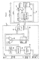
- the logic unit LU (see Fig. 4) which is part of the CPU is provided for connecting the various control means to the bus 21.
- the logic unit LU is connected to the microprocessor by a line capable of transmitting to the input VI of the microprocessor a vectored interrupt request signal VION.
- the logic unit LU comprises a decoder 46 for decoding the state signals STO-ST3 in respect of the state of the microprocessor, and emitting a signal VIAKN indicating acceptance (acknowledge) on the part of the microprocessor, of an interrupt request.
- Also connected to the logic unit LU is a group of four lines which serve for connecting the various control means to the bus 21, in daisy chain fashion.
- Each control means CONT1 ... CONT3 comprises an interrupt control circuit 47 connected to a first common line 48 of the group, by way of which the circuit 47 despatches a vectored interrupt request signal VINTA.
- the circuit 47 of the control means of class L1A (in Fig. 4, CONT1) is connected by way of an AND gate 49 to a second line of the group.
- the output of the AND gate 49 is also connected by way of a second AND gate 52 to a third line 53 of the group.
- the circuit 47 of the control means of level L 1 B (in Fig. 4, CONT2) is however connected to the line 53 by way of an AND gate 54, to which the line 51 is also directly connected.
- the ends of the lines 51 and 53 remote from the logic unit LU are connected together whereby the two sub-classes L1A and L1B form a single daisy chain.
- the printer control means CONTP is connected to the daisy chain of level L1 by way of a flip-flop 56 which is set to low level when CONTP requests an interrupt and is successively reset when the interrupt terminates, by means of a signal VIAKO, which is the negative of the acceptance signal VIAKN.
- the set outputs of the flip-flop 56 is connected to the line 51 by way of a NAND gate 57 for receiving a signal APRIO emitted by CONTP together with the interrupt request.
- the signal APRIO is also applied to an OR gate 58, the output of which is connected to another NAND gate 59.
- the other input of the NAND gate 59 is connected to the set outputs of the flip-flop 56.
- the signal APRIO is produced by a flip-flop and may be selectively '0' or '1', permanently or under control by the microprocessor. If CONTP is to be connected to the lower level of the daisy chain, that is to say the sub-class L1 B, the signal APRIO is 0: if CONTP is to be connected to the higher level of the daisy chain, that is to say, the sub-class L1A, the signal APRIO is 1.
- the circuits 47 of the control means which are enabled to request interrupts at level L2 (in Fig. 4 CONT3) are connected to a fourth line 61 of the group by way of an AND gate 62. Also connected to level L2 is a timer 63 which may be preset to emit a signal TINTO when one or more predetermined times expire.
- the signal TINTO is capable of setting a flip-flop 64, the set outputs of which is connected to a NAND gate 66.
- the flip-flop 64 is reset upon receiving the following signal VIAKN produced by the decoder 46, by way of an AND gate 65.
- the reset output R of the flip-flop 64 is connected by way of an AND gate 67 to the line 61.
- the AND gate 67 is also connected to the output of an AND gate 68 whose inputs are connected to the reset output R of the flip-flop 56, the line 53 and a line VIENO.
- the line VIENO carries a signal from the microprocessor which, when it is high, disables the chain at level L2, which can then be interrupted, whereby it represents a mask for the interrupts of level L2.
- the logic unit LU comprises an AND gate 69 capable of despatching the signal VION to the input VI of the microprocessor.
- the inputs of the AND gate 69 are respectively connected to the line 48, the NAND gate 59 and the NAND gate 66.
- CONT3 is finally connected to the output of the decoder 46, for receiving the interrupt acceptance signal VIAKN.
- the signal VINTA is at low level. It is shifted to high level when one of the units CONT1 ... CONT3, by means of the related circuit 47, requests an interrupt.
- the circuit 47 of the unit ONT1 requests the interrupt. That enables the related AND gate 49, the output of which enables the AND gate 52 which moves the output signal IEB of the line 53 to high level. If the signal APRIO is at 1 (CONTP connected with lower priority in sub-class Ll B), the signal IEB sets the output of the OR gate 58 to low level, whereby the output RINL of the gate 59 is at high level. Similarly, the output RINT of the NAND gate 66 is at high level, whereby the gate 69 transmits the signal VION to the microprocessor. The interrupt is then executed when the microprocessor, by way of the decoder 46, emits the signal VIAKN.
- any interrupt of level L2 in the presence of an interrupt of level L1, is ignored until the output of the AND gate 68 is at high level. In the absence of an interrupt at level L1, that output is at low level. If then a control unit of level L2 (in Figure 4, the unit CONT 3) requests an interrupt, the circuit 47 thereof generates the signal VINTA while, by way of the AND gate 62, it excludes arty other downstream requests (to the right of Figure 4), which are thus ignored. If the timer 63 sets the flip-flop 64 during an interrupt at level L2, the set output of the flip-flop 64 puts the output of the NAND gate 66 to high level, whereby the microprocessor receives the request from the timer 63 with the highest priority at level L2. The reset output of the flip-flop 64, by way of the AND gate 67 however enables the interrupt request at level L2.
- both the unit CONT P and the timer 63 are able to set the signal VINTA on line 48 to high level, like the other units CONT 1 ... CONT 3.
- a first region of the RAM is set up with a table T1 (see Figure 6) which will constitute the reserved region ZRM of the memory. That defines the following parameters:
- a second region of the RAM is set up with a table T2, referred to as the program state area PSA, which contains all the program state information (PSI), i.e. the flag control word (FCW) and the program counter (PC) which, following an interrupt, permit the respective execution routine to be identified and initiated.
- PSI program state information
- FCW flag control word
- PC program counter
- control byte in the register 34 ( Figure 2) can request at least one trap and the interrupts NMI, VI and NVI, there will be four PSI (see Figure 6).
- the Table T2 records the entry point (EP) of the routine associated with the corresponding vector. Therefore, in the case of NVI, NMI and TR, the microprocessor accesses to the PSA, adding to the fixed EP of the PSA, an offset established by the type of interrupt where the value of FCW and PC of the related routines is found.
- a third table T3 of the RAM (see Figure 6) is loaded with a block containing the description of each device (DDB).
- That table starts from the EPT3 indicated by ZRM and contains for each vector, the EP of the specific DDB of the interrupting device. Therefore, when two equal devices have two different vectors, beside the two vectors there will be the same DDB.
- the table T3 is not of a fixed size, but its size depends on the number of devices connected to the system.
- Another table T4 is loaded with a list which relates the logic name of each device to the associated DDB.
- the logic name is formed by a word comprising a byte for indicating the type of control unit, 4 bits for indicating the specific control unit of the same type, and 4 bits for indicating the specific device within the control unit.
- the logic name also recorded in the Table T4 is the offset in respect of the respective DDB from the EP of the table T3.
- the EP of the table T4 is derived from the table T1
- the logic name NL is found by scanning from the EP.
- the size of this table also depends on the number of devices connected to the system.
- a final table T5 is loaded into a corresponding region of the memory, with the I/O descriptions of the devices present in the system (DDB).
- DDB For each DDB, there is recorded a block of variable length, which comprises the Ep of the routine to be activated following an interrupt of class L 1A or class L1 B, the EP of the routine to be activated for an interrupt L2, other information TF, TE, TS relating to the device described, such as the specific routine which controls the orders initiated by the operating program for the control unit or device, and the like.
- the above-mentioned tables T1T5 are prepared by the microprocessor from a firmware initialisation program which is temporarily entered in the RAM and which causes the microprocessor to explore all the connections of the various control units connected to the bus 21. At the end of this operation, that program is cancelled from the RAM and replaced by other software (SW) modules, in particular the module of the operating system, thereby eliminating the virtual machine.
- SW software
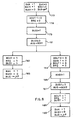
- the microprocessor When the microprocessor receives an interrupt request IREQ, before accepting it, it terminates execution of the current instruction (block 130 in Figure 7). Then, it transfers the PSI of the current program, and then the related FCW and PC, as well as the vector, in the case of a vectored interrupt routine, from the stack register R14 ( Figure 1) to a stack region of the RAM (block 131 in Figure 7). Then, the microprocessor identifies the type of interrupt or trap, with a series of decisions 132 and 133, and accesses the related table T2 of the PSA to take out the new PSI, thus initiating a new program which is the interrupt service routine.
- the microprocessor executes an interruption enabling instruction (block 147) which creates a window which permits identification of any other pending interrupts at level L1.
- the positive result of the decision leads to the decision 136, whereafter the respective routine is executed, after which a fresh window is opened.
- an interrupt disabling instruction is executed (block 148) which closes the window of the routine.
- An operation 149 is now carried out, in which the state of the registers RO-R13 is restored. The carry is again set to 0 (block 151) and the main program is re-entered (block 152) after execution of the main program re-entry code and restoration of the state of the registers and the PSI of the main program.
- each routine for execution of interruptions at level L1 comprises a head (operations 130-136), a body (operations 143-147) and a tail (148-152).
- head operations 130-136
- body operations 143-147
- tail 148-152
- the state of the registers of the main program must be saved only by the first routine. Successive routines will provide only for correcting the stack, in such a way as to keep the PSI of the main program visible. Only the routine of the last interruption will execute the tail for restoring the conditions of the main program.
- An interrupt at level L2 is executed in a similar manner to an interrupt at level L1, but without the above-mentioned time saving effect.
- the microprocessor identifies the interrupt L2, it blocks the line 61 ( Figure 4) of the level L2 with the signal VIENO, which however permits any interrupts at priority level L1 (block 153).
- the microprocessor now saves the registers RO-R13 of the main program in another portion of the region T1 of the RAM (block 154).
- Both the interrupts at level L1 and the interrupts at level L2 may be separated into two categories:
- SW software
- Such occurrences require an interruption procedure, but they do not fall into the category of vectored interrupts as referred to above, and may be processed by means of special routines independently of the vector which created them.
- Such interrupts are referred to as non-vectored interrupts (NVI) and are of lower priority than vectored interrupts.
- non-vectored interrupts are divided into four different levels, with decreasing priorities.
- a first level NV1 is reserved for services of slow units which require an execution time of more than 80 us, and services required by the peripheral units at a low frequency, such as keyboard transfer operations.
- a level NV2 reserved for services of connection as between I/O units and the system software, such as possible complementing and finalisation of an operation or predisposition of a procedure awaiting utilisation. Interrupts NV1 and NV2 are thus originated and engaged by vectored interrupts.
- Two levels NV3 and NV4 are available to the system software. Mention may be made for example of analysis of a character already accepted by the memory or the exchange of characters with a communication line, on the basis of a specific protocol, by way of a LCU unit (see Figure 1) and the related modem.
- a logic circuit 162 (see Figure 4), comprising a group of four flip-flops each associated with a level of NVI and indicated in Figure 5 by the same designation, that is to say, NV1-NV4.
- the signals from the flip-flops are applied to the microprocessor by way of a NOR gate 163.
- Another group of three flip-flops EN2-EN4 is arranged to enable the interrupt request of the corresponding flip-flops NV2-NV4 by way of three corresponding NOR gates 164, 165 and 166.
- the signals which set the flip-flops EN2-EN4 form the masks of the NVI.
- each flip-flop NV1-NV4 is associated with a corresponding queue of events, which are memorised as the various causes of interrupts as the respective levels emerge.
- level NV1 is followed in the queue by interrupts VI at level L1 for programmed IIO of slow peripheral devices.
- the level NV2 is followed by interrupts VI at level L1 and L2 for completion of an operation.
- Level NV1 for operations in respect of transfers of characters between memory and periphery, also follows the event at level NV2.
- Servicing of an interrupt NV1 is executed with the enabled vectored interrupts VI at level L1 and L2, whereby it may be interrupted by the interrupt VI.
- servicing of interrupt NV2 is executed with the interrupts VI and the interrupts NV1 which are enabled, and so forth.
- Control of the interrupts is carried out by instructions from the program, the part SF of which can assume, for the various functions, one of the values set out in the following table:
- the entry byte is of the following form:
- the engagements or bookings in respect of the interrupts NVI are extracted from the respective queues, in accordance with the above-mentioned priorities, and disposed in a register of the microprocessor ready to be examined and serviced. Such extraction operation is effected when all the interrupts are disabled, by means of suitable routines.
- the microprocessor When the microprocessor receives a request for interruption NVI, it effects saving of the PSI in the register R14, as for the vectored interrupts, and surrenders control to the routine which governs the EP of the NVI. Then, it effects saving of the registers in the stack of the system and identifies the level of the NVI. That is effected with all the NVI of higher priority and all the enabled VI, whereby it can be interrupted by the latter. When then, it resumes and concludes its service, the NVI is reset only if the respective queue is empty. In that case, a routine is performed for a fresh request for a possible interruption of lower priority.
- the units CONT 1 ... CONT 3 may be enabled for direct access to the RAM (DAM), for example in a situation of multiple character exchanges.
- the control units are connected to a pair of lines 171 and 172 of the bus 21, in accordance with a further daisy chain having maximum priority, and which extends from CONT 1 to CONT 3, imparting progressively decreasing priority to the master bus.
- each CONT comprises a circuit 173 inserted on the lines 171 and connected to the line 172.
- the line 171 is connected to the input BRQ of the microprocessor and to an OR gate 174.
- the output BAK of the microprocessor is connected to the OR gate 174, the output of which is connected by way of a NOR gate 176 to the line 172.
- a signal BUSY on the line 172 at high level indicates that the bus 21 is occupied.
- the circuit 173 sets an output signal BOUT to low level.
- the microprocessor receives the request at its input BRQ and, synchronously with the clock of the bus, emits an acceptance signal at its output BAK.
- the unit CONT which produced the request then becomes master of the bus.
- the daisy chain connection of the units CONT for control of the bus 21 is capable of resolving the conflict in the event of a request for the bus by a plurality of units CONT. It also propagates the enabling action for taking the bus in a serial mode, imparting the function of bus master to the various CONT in turn.
- the CONT which has concluded assumes lowest priority, whereby the request for the bus becomes of distributed type.
- the daisy chain mode of connection may therefore be considered as open at both sides, that is to say, connected as a ring to the microprocessor.
- control for releasing the bus is given by deactivation of the respective request signal BOUT which is then returned to high level. It was first assumed that such deactivation takes place when a CONT has finished its work, that is to say, each CONT effects multiple character exchanges in a burst mode. It will be appreciated that it is also possible to provide that at least one of or all the CONT are predisposed to exchange one character at a time, whereby the signal BOUT returns to 1 at the end of the character exchange cycle, permitting more frequent arbitration of the bus. Finally, it may be provided that at least one unit CONT consents to being interrupted by a downstream unit CONT in the daisy chain.
- the bus master permits the requesting CONT to take control of the bus, suspending the connection thereof before having exhausted its work.
- the bus master which is thus suspended may resume control of the bus when the conditions for acquisition thereof occur. That particular feature permits co-occupation on the same bus as between units CONT which exchange characters in infrequent bursts, such as magnetic disc unit control means, with which single exchanges are effected at high frequency, like high-speed line controls.
Landscapes
- Engineering & Computer Science (AREA)
- Theoretical Computer Science (AREA)
- Physics & Mathematics (AREA)
- General Engineering & Computer Science (AREA)
- General Physics & Mathematics (AREA)
- Software Systems (AREA)
- Bus Control (AREA)
Claims (7)
Applications Claiming Priority (2)
| Application Number | Priority Date | Filing Date | Title |
|---|---|---|---|
| IT68475/81A IT1145730B (it) | 1981-11-13 | 1981-11-13 | Sistema di elaborazione di dati con dispositivo di controllo delle interruzioni di programma |
| IT6847581 | 1981-11-13 |
Publications (3)
| Publication Number | Publication Date |
|---|---|
| EP0079698A2 EP0079698A2 (fr) | 1983-05-25 |
| EP0079698A3 EP0079698A3 (en) | 1985-05-22 |
| EP0079698B1 true EP0079698B1 (fr) | 1988-05-18 |
Family
ID=11309527
Family Applications (1)
| Application Number | Title | Priority Date | Filing Date |
|---|---|---|---|
| EP82305668A Expired EP0079698B1 (fr) | 1981-11-13 | 1982-10-26 | Système de traitement de données avec un dispositif pour la commande d'interruptions de programme |
Country Status (5)
| Country | Link |
|---|---|
| US (2) | US4615019A (fr) |
| EP (1) | EP0079698B1 (fr) |
| JP (1) | JPS58139255A (fr) |
| DE (1) | DE3278515D1 (fr) |
| IT (1) | IT1145730B (fr) |
Families Citing this family (20)
| Publication number | Priority date | Publication date | Assignee | Title |
|---|---|---|---|---|
| GB2173929A (en) * | 1985-04-20 | 1986-10-22 | Itt Ind Ltd | Computer systems |
| US4716523A (en) * | 1985-06-14 | 1987-12-29 | International Business Machines Corporation | Multiple port integrated DMA and interrupt controller and arbitrator |
| US4837677A (en) | 1985-06-14 | 1989-06-06 | International Business Machines Corporation | Multiple port service expansion adapter for a communications controller |
| US4751634A (en) * | 1985-06-14 | 1988-06-14 | International Business Machines Corporation | Multiple port communications adapter apparatus |
| USRE36462E (en) * | 1986-01-16 | 1999-12-21 | International Business Machines Corporation | Method to control paging subsystem processing in virtual memory data processing system during execution of critical code sections |
| US4817037A (en) * | 1987-02-13 | 1989-03-28 | International Business Machines Corporation | Data processing system with overlap bus cycle operations |
| US4953072A (en) * | 1987-05-01 | 1990-08-28 | Digital Equipment Corporation | Node for servicing interrupt request messages on a pended bus |
| DE3888353T2 (de) * | 1987-05-01 | 1994-11-17 | Digital Equipment Corp | Unterbrechungsknoten zum vorsehen von unterbrechungsanforderungen auf einem anstehenden bus. |
| DE3882991T2 (de) * | 1987-05-01 | 1994-03-24 | Digital Equipment Corp | Anordnung und methode zur erzielung von unterbrechungen mit einem "pended bus". |
| DE3740290C2 (de) * | 1987-11-27 | 1997-01-16 | Licentia Gmbh | Vorrichtung zum Steuern und/oder Regeln von Prozessen |
| US5301283A (en) * | 1992-04-16 | 1994-04-05 | Digital Equipment Corporation | Dynamic arbitration for system bus control in multiprocessor data processing system |
| US5553310A (en) * | 1992-10-02 | 1996-09-03 | Compaq Computer Corporation | Split transactions and pipelined arbitration of microprocessors in multiprocessing computer systems |
| US5535395A (en) * | 1992-10-02 | 1996-07-09 | Compaq Computer Corporation | Prioritization of microprocessors in multiprocessor computer systems |
| US5553248A (en) * | 1992-10-02 | 1996-09-03 | Compaq Computer Corporation | System for awarding the highest priority to a microprocessor releasing a system bus after aborting a locked cycle upon detecting a locked retry signal |
| US5437042A (en) * | 1992-10-02 | 1995-07-25 | Compaq Computer Corporation | Arrangement of DMA, interrupt and timer functions to implement symmetrical processing in a multiprocessor computer system |
| US5594925A (en) * | 1993-01-05 | 1997-01-14 | Texas Instruments Incorporated | Method and apparatus determining order and identity of subunits by inputting bit signals during first clock period and reading configuration signals during second clock period |
| JPH07105175A (ja) * | 1993-10-08 | 1995-04-21 | Nec Corp | マイクロコンピュータ |
| JP3242508B2 (ja) * | 1993-11-05 | 2001-12-25 | 松下電器産業株式会社 | マイクロコンピュータ |
| JPH0969047A (ja) | 1995-09-01 | 1997-03-11 | Sony Corp | Risc型マイクロプロセッサおよび情報処理装置 |
| US6023743A (en) | 1997-06-10 | 2000-02-08 | International Business Machines Corporation | System and method for arbitrating interrupts on a daisy chained architected bus |
Family Cites Families (16)
| Publication number | Priority date | Publication date | Assignee | Title |
|---|---|---|---|---|
| GB1397438A (en) * | 1971-10-27 | 1975-06-11 | Ibm | Data processing system |
| US3944985A (en) * | 1973-10-19 | 1976-03-16 | Texas Instruments Incorporated | Workspace addressing system |
| US4025904A (en) * | 1973-10-19 | 1977-05-24 | Texas Instruments Incorporated | Programmed allocation of computer memory workspace |
| IT1002275B (it) * | 1973-12-27 | 1976-05-20 | Honeywell Inf Systems | Sistema di elaborazione dati a piu canali di ingresso uscita a risorse orientate per livelli di servizio distinti e interrompi bili |
| US4159516A (en) * | 1976-03-23 | 1979-06-26 | Texas Instruments Incorporated | Input/output controller having selectable timing and maskable interrupt generation |
| US4090238A (en) * | 1976-10-04 | 1978-05-16 | Rca Corporation | Priority vectored interrupt using direct memory access |
| US4200912A (en) * | 1978-07-31 | 1980-04-29 | Motorola, Inc. | Processor interrupt system |
| US4250546A (en) * | 1978-07-31 | 1981-02-10 | Motorola, Inc. | Fast interrupt method |
| JPS5553722A (en) * | 1978-10-17 | 1980-04-19 | Toshiba Corp | Priority control system |
| JPS55121552A (en) * | 1979-03-13 | 1980-09-18 | Mitsubishi Electric Corp | Processing request control system |
| US4400694A (en) * | 1979-12-03 | 1983-08-23 | Wong Raphael W H | Microprocessor base for monitor/control of communications facilities |
| BE887134A (fr) * | 1979-12-14 | 1981-05-14 | Gte Automatic Electric Lab Inc | Circuit expanseur d'interruption |
| US4332011A (en) * | 1980-03-17 | 1982-05-25 | Cambridge Telecommunications, Inc. | Data processing arrangement including multiple groups of I/O devices with priority between groups and within each group |
| US4365294A (en) * | 1980-04-10 | 1982-12-21 | Nizdorf Computer Corporation | Modular terminal system using a common bus |
| US4414624A (en) * | 1980-11-19 | 1983-11-08 | The United States Of America As Represented By The Secretary Of The Navy | Multiple-microcomputer processing |
| US4435780A (en) * | 1981-06-16 | 1984-03-06 | International Business Machines Corporation | Separate stack areas for plural processes |
-
1981
- 1981-11-13 IT IT68475/81A patent/IT1145730B/it active
-
1982
- 1982-10-26 EP EP82305668A patent/EP0079698B1/fr not_active Expired
- 1982-10-26 DE DE8282305668T patent/DE3278515D1/de not_active Expired
- 1982-10-28 US US06/437,322 patent/US4615019A/en not_active Expired - Lifetime
- 1982-11-13 JP JP57199647A patent/JPS58139255A/ja active Pending
-
1987
- 1987-09-02 US US07/093,139 patent/US4748586A/en not_active Expired - Fee Related
Also Published As
| Publication number | Publication date |
|---|---|
| EP0079698A2 (fr) | 1983-05-25 |
| EP0079698A3 (en) | 1985-05-22 |
| IT1145730B (it) | 1986-11-05 |
| US4748586A (en) | 1988-05-31 |
| DE3278515D1 (en) | 1988-06-23 |
| JPS58139255A (ja) | 1983-08-18 |
| IT8168475A0 (it) | 1981-11-13 |
| US4615019A (en) | 1986-09-30 |
Similar Documents
| Publication | Publication Date | Title |
|---|---|---|
| US4748586A (en) | Data processing system with interrupt facilities | |
| US4420806A (en) | Interrupt coupling and monitoring system | |
| US5708814A (en) | Method and apparatus for reducing the rate of interrupts by generating a single interrupt for a group of events | |
| US5448702A (en) | Adapters with descriptor queue management capability | |
| EP0212393B1 (fr) | Système pour la gestion de plusieurs programmes de gestion d'interruption communs dans une structure de données à liste enchaînée | |
| US5784647A (en) | Interface for fetching highest priority demand from priority queue, predicting completion within time limitation then issuing demand, else adding demand to pending queue or canceling | |
| EP0241129B1 (fr) | Disposition d'adressage pour contrôleur de tampon à RAM | |
| EP0348076B1 (fr) | Dispositif de traitement de données | |
| US4200912A (en) | Processor interrupt system | |
| GB1170285A (en) | A Modular Multicomputing Data Processing System | |
| EP0446077B1 (fr) | Système de contrÔle pour un système multiprocesseur | |
| CA2007737C (fr) | Operations de transfert de donnees entre deux bus asynchrones | |
| US3639911A (en) | Digital processor having automatic conflict-resolving logic | |
| US5944788A (en) | Message transfer system and control method for multiple sending and receiving modules in a network supporting hardware and software emulated modules | |
| US7617389B2 (en) | Event notifying method, event notifying device and processor system permitting inconsistent state of a counter managing number of non-notified events | |
| US5999969A (en) | Interrupt handling system for message transfers in network having mixed hardware and software emulated modules | |
| EP0049158B1 (fr) | Système de traitement des données entrée/sortie | |
| US4225917A (en) | Error driven interrupt for polled MPU systems | |
| US4561053A (en) | Input/output multiplexer for a data processing system | |
| US5842003A (en) | Auxiliary message arbitrator for digital message transfer system in network of hardware modules | |
| CA2022073A1 (fr) | Appareil et methode de reception de donnees d'etat de communication serie au moyen d'un controleur a acces direct memoire | |
| CA1167986A (fr) | Multiplexeur de communication partageant une minuterie libre entre plusieurs lignes de communication | |
| Feinroth et al. | Telecommunications using a front-end minicomputer | |
| JPS63268035A (ja) | ロ−カル端末シミユレ−タによるリモ−ト端末制御方式 | |
| JPS62192844A (ja) | Dma制御回路 |
Legal Events
| Date | Code | Title | Description |
|---|---|---|---|
| PUAI | Public reference made under article 153(3) epc to a published international application that has entered the european phase |
Free format text: ORIGINAL CODE: 0009012 |
|
| AK | Designated contracting states |
Designated state(s): DE FR GB |
|
| PUAL | Search report despatched |
Free format text: ORIGINAL CODE: 0009013 |
|
| AK | Designated contracting states |
Designated state(s): DE FR GB |
|
| 17P | Request for examination filed |
Effective date: 19851022 |
|
| 17Q | First examination report despatched |
Effective date: 19870109 |
|
| D17Q | First examination report despatched (deleted) | ||
| GRAA | (expected) grant |
Free format text: ORIGINAL CODE: 0009210 |
|
| AK | Designated contracting states |
Kind code of ref document: B1 Designated state(s): DE FR GB |
|
| REF | Corresponds to: |
Ref document number: 3278515 Country of ref document: DE Date of ref document: 19880623 |
|
| ET | Fr: translation filed | ||
| PLBE | No opposition filed within time limit |
Free format text: ORIGINAL CODE: 0009261 |
|
| STAA | Information on the status of an ep patent application or granted ep patent |
Free format text: STATUS: NO OPPOSITION FILED WITHIN TIME LIMIT |
|
| 26N | No opposition filed | ||
| PGFP | Annual fee paid to national office [announced via postgrant information from national office to epo] |
Ref country code: FR Payment date: 19971009 Year of fee payment: 16 |
|
| PGFP | Annual fee paid to national office [announced via postgrant information from national office to epo] |
Ref country code: DE Payment date: 19971031 Year of fee payment: 16 |
|
| PG25 | Lapsed in a contracting state [announced via postgrant information from national office to epo] |
Ref country code: FR Free format text: LAPSE BECAUSE OF NON-PAYMENT OF DUE FEES Effective date: 19990630 |
|
| REG | Reference to a national code |
Ref country code: FR Ref legal event code: ST |
|
| PG25 | Lapsed in a contracting state [announced via postgrant information from national office to epo] |
Ref country code: DE Free format text: LAPSE BECAUSE OF NON-PAYMENT OF DUE FEES Effective date: 19990803 |
|
| PGFP | Annual fee paid to national office [announced via postgrant information from national office to epo] |
Ref country code: GB Payment date: 19991020 Year of fee payment: 18 |
|
| PG25 | Lapsed in a contracting state [announced via postgrant information from national office to epo] |
Ref country code: GB Free format text: LAPSE BECAUSE OF NON-PAYMENT OF DUE FEES Effective date: 20001026 |
|
| GBPC | Gb: european patent ceased through non-payment of renewal fee |
Effective date: 20001026 |