EP0079775A2 - Schutz gegen falsche Signalerzeugung in Halbleiteranordnungen - Google Patents
Schutz gegen falsche Signalerzeugung in Halbleiteranordnungen Download PDFInfo
- Publication number
- EP0079775A2 EP0079775A2 EP82306038A EP82306038A EP0079775A2 EP 0079775 A2 EP0079775 A2 EP 0079775A2 EP 82306038 A EP82306038 A EP 82306038A EP 82306038 A EP82306038 A EP 82306038A EP 0079775 A2 EP0079775 A2 EP 0079775A2
- Authority
- EP
- European Patent Office
- Prior art keywords
- signal lines
- semiconductor substrate
- group
- input signal
- semiconductor
- Prior art date
- Legal status (The legal status is an assumption and is not a legal conclusion. Google has not performed a legal analysis and makes no representation as to the accuracy of the status listed.)
- Granted
Links
Images

Classifications
-
- H—ELECTRICITY
- H10—SEMICONDUCTOR DEVICES; ELECTRIC SOLID-STATE DEVICES NOT OTHERWISE PROVIDED FOR
- H10W—GENERIC PACKAGES, INTERCONNECTIONS, CONNECTORS OR OTHER CONSTRUCTIONAL DETAILS OF DEVICES COVERED BY CLASS H10
- H10W42/00—Arrangements for protection of devices
- H10W42/60—Arrangements for protection of devices protecting against electrostatic charges or discharges, e.g. Faraday shields
-
- H—ELECTRICITY
- H10—SEMICONDUCTOR DEVICES; ELECTRIC SOLID-STATE DEVICES NOT OTHERWISE PROVIDED FOR
- H10W—GENERIC PACKAGES, INTERCONNECTIONS, CONNECTORS OR OTHER CONSTRUCTIONAL DETAILS OF DEVICES COVERED BY CLASS H10
- H10W20/00—Interconnections in chips, wafers or substrates
- H10W20/40—Interconnections external to wafers or substrates, e.g. back-end-of-line [BEOL] metallisations or vias connecting to gate electrodes
- H10W20/41—Interconnections external to wafers or substrates, e.g. back-end-of-line [BEOL] metallisations or vias connecting to gate electrodes characterised by their conductive parts
- H10W20/423—Shielding layers
Definitions
- the present invention relates to protection against erroneous signal generation in semiconductor devices.
- An erroneous signal may be produced, for example, in a semiconductor memory device, as a result of a potential change on input signal lines being transferred to bit lines of the device.
- each sense amplifier should nowadays be able to detect the small potential difference of about 100 mV generated between pairs of bit lines. This has been necessitated by the decrease in individual cell capacities accompanying higher degrees of integration.
- Such a high-sensitivity sense amplifier may be rather susceptible to error operations due to noise. This is especially possible when the potentials of the input signals, for example address signals, are changed at the same time as sense amplifiers operate, or just before the operation of the sense amplifiers. This change can influence the potentials of the bit lines through parasitic electrostatic capacitances, as hereinafter described in more detail, causing error operations of the sense amplifiers.
- An embodiment of the present invention can be constructed in the form of a semiconductor device comprising a semiconductor substrate, a first group of signal lines, and a second group of signal lines.
- the first group and second group are arranged on different positions on the semiconductor substrate.
- the device further comprises an electrostatic shield layer for the semiconductor substrate, formed under at least one of the first and second groups of signal lines.
- FIG. 1 shows a general structure of a conventional dynamic semiconductor memory device.
- a dynamic semiconductor memory chip CH includes in its central portion a plurality of sense amplifiers SA 1 , SA 2 , ..., Sa i , ...., and SA n . To the right and left of each sense amplifier extend a pair of bit lines BL and BL respectively. For the purpose of simplicity, only one pair of bit lines is illustrated.
- the bit lines BL and BL are connected to memory cells (not shown) arranged in memory cell arrays 1 and 1'.
- Reference numerals 2 and 2' represent peripheral circuits of, for example, decoders or buffer amplifiers.
- Reference numerals 3 and 3' are input signal lines connected to input terminals A 0 , A 1 , A 2 , A 31 A4 and A 5 .
- the input terminals A O through A 5 receive input signals of, for example, address input signals or data. All of the above elements and lines are formed on a semiconductor substrate 4.
- the bit lines BL and BL are diffusion layers formed at the surface of the semiconductor substrate 4 or wiring layers of, for example, polysilicon formed on the semiconductor substrate through an insulating layer (not shown). Therefore, in both cases, an electrostatic capacitance is formed between each bit line BL or BL and the semiconductor substrate 4. When the bit lines BL and BL are formed by diffusion layers, the electrostatic capacitance is greater than that when the bit lines BL and BL are formed by polysilicon or aluminum..
- the input signal lines 3 and 3' are wiring layers of, for example, aluminum formed on the substrate 4 through an insulating layer (not shown in Figure 1). Therefore, an electrostatic capacitance is also formed between each input signal line and the semiconductor substrate 4.
- bit lines BL and BL are formed as diffusion layers at the surface of the semiconductor substrate 4.
- the input signal lines 3 and 3' extend in an insulating layer 5 formed on the semiconductor substrate 4.
- An equivalent circuit, showing the electrical relationship among the bit lines BL and BL, the semiconductor substrate 4, and the input signal lines 3 and 3', is also illustrated in Fig. 2.
- each input signal line 3 and the semiconductor substrate 4 there is an electrostatic capacitance C 0 , C, , or C 2 .
- an electrostatic capacitance C 3 , C 4 , or C 5 is formed between each input signal line 3' and the semiconductor substrate 4.
- the bit lines BL and BL and the semiconductor substrate 4 there are electrostatic capacitances C and C 7 , respectively. Since the semiconductor substrate 4 has a resistance, a resistance R is illustrated between the capacitances C 6 and C 7 .
- N 0 through N 7 in the semiconductor substrate 4 are nodes connected to these capacitances C 0 through C 7 , respectively.
- the potential of the semiconductor substrate is influenced by the potential of the input signal lines 3 and 3'.
- the potentials of the input signal lines 3 and 3' are changed by changing the address signals or data applied to the input terminals A 0 through A 5 , the potentials at the nodes N 0 through N 5 in the semiconductor substrate 4 are also changed.
- the potentials of both groups of the input signal lines 3 and 3' are changed simultaneously in the same direction, i.e., from a high (H) level to a low (L) level or from a low (L) level to a high (H) level, and if the number of the input signal lines 3 is the same as the number of the input signal lines 3', no problem will occur.
- the potential of the bit line BL Due to the presence of the capacitance C 6 , the potential of the bit line BL is boosted. Also, due to the presence of the capacitance C 7' the potential of the bit line BL is lowered. Since the nodes N 6 and N 7 are separated by the resistance R, the potentials of the nodes N 6 and N 7 can not be equilibrated for a definite period due to the presence of the resistance R. Thus, the maximum potential difference is produced between the bit lines BL and BL. Assume that the actual data stored in a memory cell is one for increasing the potential of the bit line BL over the potential of the bit line BL.
- the capacitances C 0 through C 7 may conversely make the potential of the bit line BL higher than the potential of the bit line BL, causing the sense amplifier SA i to detect erroneous data.
- the signals to be applied to the input signal lines can take any value. That is, it is not predetermined what type of signals they are, i.e., what combination of the H levels and L levels they are. Depending on the combination of the input signals, it is possible that the potential difference between the bit lines BL and BL due to the capacitances C through C 7 will become sufficiently large to cause an error reading of the sense amplifier SA..
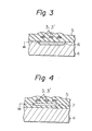
- Figure 3 is a cross-section of a part of a dynamic semiconductor memory device according to a first embodiment of the invention.
- the input signal lines 3 or 3', the semiconductor substrate 4, and the insulating layer 5 are the same as those in Fig. 2.
- the difference between Figs. 2 and 3 is that, in Fig. 3, a diffusion layer 6 of a conductivity type opposite to that of the semiconductor substrate 4 is formed at the surface of the semiconductor substrate 4 and under the input signal lines 3 or 3'.
- the diffusion layer 6 is connected to the ground.
- the diffusion layer 6 may be connected to a power supply (not shown).
- the diffusion layer 6 may be formed under one group of the input signal lines 3 or 3' or under both groups of the input signal lines 3 and 3'.
- Figure 4 illustrates another embodiment of the present invention.
- a wiring layer 7, made of a good conductor such as polysilicon, aluminum, molybdenum (Mo), or molybdenum--silicide (MoSi ) is formed in the insulating layer 5 and under the input signal lines 3 or 3'.
- the wiring layer 7 is also connected to the ground or to a power supply.
- the wiring layer 7 may also be formed under one group of the input signal lines 3 or 3', or under both groups of the input signal lines 3 and 3'.
- the diffusion layer 6 in Fig. 3 and the wiring layer 7 in Fig. 4 act as electrostatic shield layers, respectively, of the input signal lines 3 and/or 3' for the semiconductor substrate 4. Accordingly, changes of the potentials at the input signal lines 3 and 3' by external input signals have no effect on the potential of the semiconductor substrate 4. Therefore, little or no potential difference is produced between the bit lines BL and BL in response to the potential change of the input signal lines 3 and 3'. Thus, error reading by the sense amplifier in the dynamic semiconductor memory device can be protected against.
- a shielding layer such as layers 6 and 7 is also effective in other static semiconductor memory devices, code converters (CODEC), and many other semiconductor devices.
- the shielding layer may be formed under the bit lines and on or at the surface of the semiconductor substrate, in an embodiment of the invention.
Landscapes
- Semiconductor Memories (AREA)
- Semiconductor Integrated Circuits (AREA)
Applications Claiming Priority (2)
| Application Number | Priority Date | Filing Date | Title |
|---|---|---|---|
| JP56182114A JPS5884455A (ja) | 1981-11-13 | 1981-11-13 | 半導体記憶装置 |
| JP182114/81 | 1981-11-13 |
Publications (3)
| Publication Number | Publication Date |
|---|---|
| EP0079775A2 true EP0079775A2 (de) | 1983-05-25 |
| EP0079775A3 EP0079775A3 (en) | 1985-12-18 |
| EP0079775B1 EP0079775B1 (de) | 1989-04-26 |
Family
ID=16112572
Family Applications (1)
| Application Number | Title | Priority Date | Filing Date |
|---|---|---|---|
| EP82306038A Expired EP0079775B1 (de) | 1981-11-13 | 1982-11-12 | Schutz gegen falsche Signalerzeugung in Halbleiteranordnungen |
Country Status (3)
| Country | Link |
|---|---|
| EP (1) | EP0079775B1 (de) |
| JP (1) | JPS5884455A (de) |
| DE (1) | DE3279659D1 (de) |
Cited By (13)
| Publication number | Priority date | Publication date | Assignee | Title |
|---|---|---|---|---|
| FR2565031A1 (fr) * | 1984-05-25 | 1985-11-29 | Labo Electronique Physique | Procede de realisation d'un blindage entre deux sous-ensembles d'un microcircuit et application de ce procede a la realisation d'un circuit integre monolithique comprenant deux sous-ensembles ainsi isoles |
| EP0163795A3 (de) * | 1983-12-13 | 1987-04-15 | Fairchild Semiconductor Corporation | Verfahren und Mittel zur Reduzierung von Signal-Fortpflanzungsverluste in ausserhochintegrierte Schaltungen |
| DE3706251A1 (de) * | 1986-02-28 | 1987-09-03 | Canon Kk | Halbleitervorrichtung |
| EP0256850A3 (de) * | 1986-08-12 | 1988-08-10 | Canon Kabushiki Kaisha | Photoelektrischer Wandler |
| EP0270184A3 (de) * | 1986-12-03 | 1989-01-04 | Philips Patentverwaltung GmbH | Integrierte Halbleiter-Schaltung mit Mehrlagenverdrahtung |
| EP0298576A1 (de) * | 1987-07-10 | 1989-01-11 | Koninklijke Philips Electronics N.V. | Ladungsverschiebeanordnung |
| US4833521A (en) * | 1983-12-13 | 1989-05-23 | Fairchild Camera & Instrument Corp. | Means for reducing signal propagation losses in very large scale integrated circuits |
| US4922117A (en) * | 1987-06-12 | 1990-05-01 | Canon Kabushiki Kaisha | Photoelectric conversion device having a constant potential wiring at the sides of the common wiring |
| US5338690A (en) * | 1986-01-24 | 1994-08-16 | Canon Kabushiki Kaisha | Photoelectronic conversion device |
| FR2726941A1 (fr) * | 1986-01-28 | 1996-05-15 | Cimsa Cintra | Dispositif integre de protection par varistance d'un composant electronique contre les effets d'un champ electro-magnetique ou de charges statiques |
| US5594279A (en) * | 1992-11-12 | 1997-01-14 | Texas Instruments Incorporated | Semiconductor device having shield wiring for noise suppression |
| EP0917202A1 (de) * | 1997-11-12 | 1999-05-19 | Lsi Logic Corporation | Eingebetteter Speicher mit elektromagnetischer Abschirmung beinhaltender integrierter Schaltkreis |
| US6069393A (en) * | 1987-06-26 | 2000-05-30 | Canon Kabushiki Kaisha | Photoelectric converter |
Families Citing this family (1)
| Publication number | Priority date | Publication date | Assignee | Title |
|---|---|---|---|---|
| AT502716B1 (de) * | 2005-11-09 | 2007-10-15 | Robert Swoboda | Struktur und schaltung zur vermeidung des einflusses der parasitären kapazitiven substrat- kopplung von integrierten widerständen |
Family Cites Families (5)
| Publication number | Priority date | Publication date | Assignee | Title |
|---|---|---|---|---|
| FR1471729A (fr) * | 1965-03-19 | 1967-03-03 | Rca Corp | Dispositif semi-conducteur |
| US3602782A (en) * | 1969-12-05 | 1971-08-31 | Thomas Klein | Conductor-insulator-semiconductor fieldeffect transistor with semiconductor layer embedded in dielectric underneath interconnection layer |
| US3841926A (en) * | 1973-01-02 | 1974-10-15 | Ibm | Integrated circuit fabrication process |
| US3990102A (en) * | 1974-06-28 | 1976-11-02 | Hitachi, Ltd. | Semiconductor integrated circuits and method of manufacturing the same |
| DE2522984C2 (de) * | 1975-05-23 | 1983-06-01 | Licentia Patent-Verwaltungs-Gmbh, 6000 Frankfurt | Elektronischer Koppelpunktbaustein |
-
1981
- 1981-11-13 JP JP56182114A patent/JPS5884455A/ja active Pending
-
1982
- 1982-11-12 DE DE8282306038T patent/DE3279659D1/de not_active Expired
- 1982-11-12 EP EP82306038A patent/EP0079775B1/de not_active Expired
Cited By (18)
| Publication number | Priority date | Publication date | Assignee | Title |
|---|---|---|---|---|
| EP0163795A3 (de) * | 1983-12-13 | 1987-04-15 | Fairchild Semiconductor Corporation | Verfahren und Mittel zur Reduzierung von Signal-Fortpflanzungsverluste in ausserhochintegrierte Schaltungen |
| US4833521A (en) * | 1983-12-13 | 1989-05-23 | Fairchild Camera & Instrument Corp. | Means for reducing signal propagation losses in very large scale integrated circuits |
| FR2565031A1 (fr) * | 1984-05-25 | 1985-11-29 | Labo Electronique Physique | Procede de realisation d'un blindage entre deux sous-ensembles d'un microcircuit et application de ce procede a la realisation d'un circuit integre monolithique comprenant deux sous-ensembles ainsi isoles |
| US5338690A (en) * | 1986-01-24 | 1994-08-16 | Canon Kabushiki Kaisha | Photoelectronic conversion device |
| FR2726941A1 (fr) * | 1986-01-28 | 1996-05-15 | Cimsa Cintra | Dispositif integre de protection par varistance d'un composant electronique contre les effets d'un champ electro-magnetique ou de charges statiques |
| DE3706251A1 (de) * | 1986-02-28 | 1987-09-03 | Canon Kk | Halbleitervorrichtung |
| US5150189A (en) * | 1986-02-28 | 1992-09-22 | Canon Kabushiki Kaisha | Semiconductor apparatus |
| US5027176A (en) * | 1986-08-12 | 1991-06-25 | Canon Kabushiki Kaisha | Photo-electric converter with intervening wirings for capacitive shielding |
| EP0256850A3 (de) * | 1986-08-12 | 1988-08-10 | Canon Kabushiki Kaisha | Photoelektrischer Wandler |
| EP0270184A3 (de) * | 1986-12-03 | 1989-01-04 | Philips Patentverwaltung GmbH | Integrierte Halbleiter-Schaltung mit Mehrlagenverdrahtung |
| US4939592A (en) * | 1987-06-12 | 1990-07-03 | Canon Kabushiki Kaisha | Contact photoelectric conversion device |
| US4922117A (en) * | 1987-06-12 | 1990-05-01 | Canon Kabushiki Kaisha | Photoelectric conversion device having a constant potential wiring at the sides of the common wiring |
| US6069393A (en) * | 1987-06-26 | 2000-05-30 | Canon Kabushiki Kaisha | Photoelectric converter |
| EP0298576A1 (de) * | 1987-07-10 | 1989-01-11 | Koninklijke Philips Electronics N.V. | Ladungsverschiebeanordnung |
| US5594279A (en) * | 1992-11-12 | 1997-01-14 | Texas Instruments Incorporated | Semiconductor device having shield wiring for noise suppression |
| KR100320057B1 (ko) * | 1992-11-12 | 2002-03-21 | 윌리엄 비. 켐플러 | 반도체장치 |
| EP0917202A1 (de) * | 1997-11-12 | 1999-05-19 | Lsi Logic Corporation | Eingebetteter Speicher mit elektromagnetischer Abschirmung beinhaltender integrierter Schaltkreis |
| US6166403A (en) * | 1997-11-12 | 2000-12-26 | Lsi Logic Corporation | Integrated circuit having embedded memory with electromagnetic shield |
Also Published As
| Publication number | Publication date |
|---|---|
| JPS5884455A (ja) | 1983-05-20 |
| DE3279659D1 (en) | 1989-06-01 |
| EP0079775A3 (en) | 1985-12-18 |
| EP0079775B1 (de) | 1989-04-26 |
Similar Documents
| Publication | Publication Date | Title |
|---|---|---|
| JP5039403B2 (ja) | 平面状にアクセスラインを具備したメモリセル | |
| US5933364A (en) | Semiconductor device with a metal layer for supplying a predetermined potential to a memory cell section | |
| EP0079775A2 (de) | Schutz gegen falsche Signalerzeugung in Halbleiteranordnungen | |
| US5045899A (en) | Dynamic random access memory having stacked capacitor structure | |
| US6741492B2 (en) | Semiconductor memory device | |
| US4551820A (en) | Dynamic RAM integrated circuit device | |
| GB2087183A (en) | Semiconductor integrated circuit device | |
| EP0169332A2 (de) | Hochverdichtete Speicher mit Einzelelementspeicherzellen | |
| KR19990044140A (ko) | 메모리 장치 및 그 배치를 최소화하기 위한 방법 | |
| US4809046A (en) | Semiconductor memory device | |
| US5206533A (en) | Transistor device with resistive coupling | |
| US6285208B1 (en) | Activation speed of signal wiring line in semiconductor integrated circuit | |
| EP0081368B1 (de) | Halbleiterspeicheranlage | |
| EP0098156B1 (de) | Dynamische Halbleiterspeicheranordnung | |
| KR19990029197A (ko) | 반도체 기억 장치 | |
| EP0506989B1 (de) | Eine nichtflüchtige Halbleiterspeicheranordnung, die eine differentielle Zelle als Speicherzelle gebraucht | |
| US5535153A (en) | Semiconductor device | |
| GB2149250A (en) | Dynamic memory | |
| JPS6035755B2 (ja) | センス増幅器 | |
| US6285573B1 (en) | Semiconductor integrated circuit having shield wire | |
| US5670815A (en) | Layout for noise reduction on a reference voltage | |
| KR19980081691A (ko) | 칩면적 및 소비 전력을 감소시킬 수 있는 반도체 집적회로 장치 | |
| KR19990078452A (ko) | 노이즈 방지 차폐 도전체를 가진 내장 다이내믹 랜덤 액세스 메모리 | |
| EP0281868B1 (de) | Halbleiter-Speichereinrichtung mit Schutzzellen | |
| US5153699A (en) | Semiconductor device |
Legal Events
| Date | Code | Title | Description |
|---|---|---|---|
| PUAI | Public reference made under article 153(3) epc to a published international application that has entered the european phase |
Free format text: ORIGINAL CODE: 0009012 |
|
| AK | Designated contracting states |
Designated state(s): DE FR GB |
|
| PUAL | Search report despatched |
Free format text: ORIGINAL CODE: 0009013 |
|
| AK | Designated contracting states |
Designated state(s): DE FR GB |
|
| 17P | Request for examination filed |
Effective date: 19860131 |
|
| 17Q | First examination report despatched |
Effective date: 19870513 |
|
| GRAA | (expected) grant |
Free format text: ORIGINAL CODE: 0009210 |
|
| AK | Designated contracting states |
Kind code of ref document: B1 Designated state(s): DE FR GB |
|
| REF | Corresponds to: |
Ref document number: 3279659 Country of ref document: DE Date of ref document: 19890601 |
|
| ET | Fr: translation filed | ||
| PLBE | No opposition filed within time limit |
Free format text: ORIGINAL CODE: 0009261 |
|
| STAA | Information on the status of an ep patent application or granted ep patent |
Free format text: STATUS: NO OPPOSITION FILED WITHIN TIME LIMIT |
|
| 26N | No opposition filed | ||
| PGFP | Annual fee paid to national office [announced via postgrant information from national office to epo] |
Ref country code: GB Payment date: 19920903 Year of fee payment: 11 |
|
| PGFP | Annual fee paid to national office [announced via postgrant information from national office to epo] |
Ref country code: FR Payment date: 19921127 Year of fee payment: 11 |
|
| PGFP | Annual fee paid to national office [announced via postgrant information from national office to epo] |
Ref country code: DE Payment date: 19930129 Year of fee payment: 11 |
|
| PG25 | Lapsed in a contracting state [announced via postgrant information from national office to epo] |
Ref country code: GB Effective date: 19931112 |
|
| GBPC | Gb: european patent ceased through non-payment of renewal fee |
Effective date: 19931112 |
|
| PG25 | Lapsed in a contracting state [announced via postgrant information from national office to epo] |
Ref country code: FR Effective date: 19940729 |
|
| PG25 | Lapsed in a contracting state [announced via postgrant information from national office to epo] |
Ref country code: DE Effective date: 19940802 |
|
| REG | Reference to a national code |
Ref country code: FR Ref legal event code: ST |