EP0079848A2 - Dispositif pour dessouder des composants électroniques des circuits imprimés - Google Patents
Dispositif pour dessouder des composants électroniques des circuits imprimés Download PDFInfo
- Publication number
- EP0079848A2 EP0079848A2 EP82730132A EP82730132A EP0079848A2 EP 0079848 A2 EP0079848 A2 EP 0079848A2 EP 82730132 A EP82730132 A EP 82730132A EP 82730132 A EP82730132 A EP 82730132A EP 0079848 A2 EP0079848 A2 EP 0079848A2
- Authority
- EP
- European Patent Office
- Prior art keywords
- housing
- circuit board
- printed circuit
- compressed air
- solder
- Prior art date
- Legal status (The legal status is an assumption and is not a legal conclusion. Google has not performed a legal analysis and makes no representation as to the accuracy of the status listed.)
- Granted
Links
- 229910000679 solder Inorganic materials 0.000 claims abstract description 47
- 238000005476 soldering Methods 0.000 claims abstract description 6
- 238000002844 melting Methods 0.000 claims description 12
- 230000008018 melting Effects 0.000 claims description 12
- 230000002093 peripheral effect Effects 0.000 claims description 4
- 230000009471 action Effects 0.000 abstract description 4
- 239000012530 fluid Substances 0.000 description 7
- 238000007664 blowing Methods 0.000 description 5
- 230000006835 compression Effects 0.000 description 2
- 238000007906 compression Methods 0.000 description 2
- 238000010586 diagram Methods 0.000 description 2
- 230000000694 effects Effects 0.000 description 2
- 238000010438 heat treatment Methods 0.000 description 2
- 238000004519 manufacturing process Methods 0.000 description 2
- 230000000284 resting effect Effects 0.000 description 2
- QILUYCYPNYWMIL-UHFFFAOYSA-N 1,2,3-trichloro-5-(2-chlorophenyl)benzene Chemical compound ClC1=C(Cl)C(Cl)=CC(C=2C(=CC=CC=2)Cl)=C1 QILUYCYPNYWMIL-UHFFFAOYSA-N 0.000 description 1
- OKTJSMMVPCPJKN-UHFFFAOYSA-N Carbon Chemical group [C] OKTJSMMVPCPJKN-UHFFFAOYSA-N 0.000 description 1
- 229910000639 Spring steel Inorganic materials 0.000 description 1
- 230000008859 change Effects 0.000 description 1
- 238000004140 cleaning Methods 0.000 description 1
- 238000010276 construction Methods 0.000 description 1
- 230000008878 coupling Effects 0.000 description 1
- 238000010168 coupling process Methods 0.000 description 1
- 238000005859 coupling reaction Methods 0.000 description 1
- 230000001419 dependent effect Effects 0.000 description 1
- 229910002804 graphite Inorganic materials 0.000 description 1
- 239000010439 graphite Substances 0.000 description 1
- 239000000155 melt Substances 0.000 description 1
- 230000009467 reduction Effects 0.000 description 1
- 230000000717 retained effect Effects 0.000 description 1
- 238000007789 sealing Methods 0.000 description 1
Images




Classifications
-
- H—ELECTRICITY
- H05—ELECTRIC TECHNIQUES NOT OTHERWISE PROVIDED FOR
- H05K—PRINTED CIRCUITS; CASINGS OR CONSTRUCTIONAL DETAILS OF ELECTRIC APPARATUS; MANUFACTURE OF ASSEMBLAGES OF ELECTRICAL COMPONENTS
- H05K13/00—Apparatus or processes specially adapted for manufacturing or adjusting assemblages of electric components
- H05K13/04—Mounting of components, e.g. of leadless components
- H05K13/0486—Replacement and removal of components
-
- H—ELECTRICITY
- H05—ELECTRIC TECHNIQUES NOT OTHERWISE PROVIDED FOR
- H05K—PRINTED CIRCUITS; CASINGS OR CONSTRUCTIONAL DETAILS OF ELECTRIC APPARATUS; MANUFACTURE OF ASSEMBLAGES OF ELECTRICAL COMPONENTS
- H05K13/00—Apparatus or processes specially adapted for manufacturing or adjusting assemblages of electric components
- H05K13/04—Mounting of components, e.g. of leadless components
Definitions
- the invention relates to a device for unsoldering electronic components from printed circuit boards according to the preamble of claim 1.
- an electronic component to be desoldered is clamped by means of the resilient gripping pliers by pushing the housing along the pull rod over part of the legs of the resilient gripping pliers, whereby the component is pinched by the gripper.
- the device for melting the solder joints is located below the circuit board carrying the component to be soldered and consists of heated rings into which the solder joints to be melted engage.
- the mouth is located between the grooves as a device for removing solder residues from the holes in the printed circuit board a vacuum device.
- This known device for unsoldering electronic components from printed circuit boards is extremely complex, in particular with regard to the arrangement and design of the device for removing solder residues from the holes in the printed circuit board in the form of a vacuum device, and in particular requires a very special design of the device for melting the solder joints.
- the head After lifting the head and removing the removed component, the head is placed on the printed circuit board in a sealing manner and the holes in the printed circuit board are freed of solder residues under the effect of compressed air flowing through the head.
- the device requires both a vacuum and a compressed air device for the pulling head and on the other hand, this known device requires two separate operations for removing the soldered component and for blowing out the holes in the circuit board.
- the invention has for its object to provide a device for desoldering electronic components from printed circuit boards of the generic type, which with a simple and inexpensive construction, the removal of a soldered component and the removal of solder residues from the holes in the circuit board in a simple manner and in allows one and the same operation from the top of the worktop.
- the spring-loaded drawbar pulls the soldered component using the spring-loaded gripper further into the housing of the resilient gripping pliers, whereupon compressed air for blowing out the holes in the printed circuit board can be supplied immediately via the compressed air line connected to the housing and connected to a compressed air source.
- the inner walls of the housing serve on the one hand to guide the resilient gripping pliers and on the other hand to form a sealed compressed air space, so that the compressed air can only escape through the holes of the printed circuit board that are cleared of the component legs when the lower, peripheral edge of the housing rests on the printed circuit board these are completely cleaned of solder residues.
- the device according to the invention is extremely simple and inexpensive to manufacture, since both functions of removing a component from the circuit board and removing solder residues from the holes in the circuit board are effected by one and the same component, namely the housing in connection with the resilient gripping pliers . Both operations take place from the top of the circuit board and one after the other in time, so that a quick work operation is possible. In contrast to the prior art described in the introduction, it is not necessary to remove the soldered electronic component from the housing or from the resilient gripping pliers before blowing out the holes in the printed circuit board, which enables shortest working hours.
- the device according to the invention can cooperate with a simple solder bath wave to be arranged underneath the circuit board, without this having to be provided in an expensive and complex manner with a device for removing solder residues from the holes in the circuit board.
- the device according to the invention is detachably fastened transversely to and on a swivel arm which can be swiveled about an axis from a horizontal soldering position into a vertical assembly position.
- the component to be unsoldered which is still on the circuit board, can be clamped in a comfortable working position by the operator by means of the resilient gripping pliers and at the same time sealed by the housing of the resilient gripping pliers.
- the device for melting the solder joints and the pulling device, as well as the device for removing solder residues from the holes in the printed circuit board can be activated electronically one after the other fully automatically.
- hot air is supplied to the housing for the resilient gripping pliers itself in order to melt the soldering points with it.
- the device then automatically carries out the work operations of removing the component to be unsoldered and blowing out the circuit board holes.
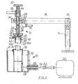
- the device for unsoldering electronic components from printed circuit boards essentially comprises two structural units, namely a device 10 for melting the solder joints and a device 12 for removing an electronic component from a printed circuit board and at the same time for removing solder residues from the holes in the printed circuit board.
- the removal and solder removal device 12 is attached to a frame 14 which has a swivel joint 16 which can be swiveled about a horizontal axis and to which a swivel arm 18 is fastened, which can either be in a vertical assembly position according to FIG. 1 or in a horizontal unsoldering position according to the figures 2 and 3 can be brought.
- a receiving slot 20 is arranged transversely to the longitudinal axis of the swivel arm 18, which serves for the releasable arrangement of the pulling device 22 , which is held in the swivel arm 18 by means of a screw 24.
- the pulling device 22 comprises a carrier sleeve 26 with a longitudinal bore 28 extending axially therein.
- a pull rod 30 is arranged within the longitudinal bore 28 and carries an actuating handle 32 at its upper end.
- Compression spring 34 is arranged, which holds the pull rod 30 in its upper actuation position, as shown in Figures 2 and 3.
- an approximately perpendicularly projecting handle bar 33 is attached to it, which, in cooperation with the actuating handle 32, enables one-hand operation for the pull bar 30.
- the pull rod 30 ends at its lower end in the illustration according to FIGS. 2 and 3 in a resilient gripping pliers 36 for electronic components.
- This resilient gripper 36 consists of a curved leaf spring made of spring steel, which is fixed approximately in the middle by means of a screw 38 and a curve piece 40 at the lower end of the pull rod 30.
- the resilient gripper 36 has at both ends inwardly projecting lugs 42 for reaching under the ends of an electronic component, such as. B. an IC element, in particular those ends of this component at which no component legs are arranged, i.e. on the short sides.
- the resilient gripping pliers 36 can also be designed such that they grip around the long sides of an electronic component to which the component legs are attached.
- the two arms 44 of the resilient gripping pliers which carry the inwardly projecting lugs 42, have a tendency to come together bend outwards and are retained by a housing 46, the inner narrow sides of which serve as guides for the arms 44 of the resilient gripping pliers 36 and at the same time for closing them.
- the housing 46 is fastened to a housing carrier 48 which is fixedly connected to the carrier sleeve 26.
- the cross-sectional dimensions of the housing 46 can be adapted to the cross-sectional dimensions of the electronic components to be soldered and removed by means of housings 46 with different cross sections, which can be exchangeably fastened to the pull rod 30 by means of a screw 50.
- a fluid line is provided through the carrier sleeve 26 adjacent to the pull rod 30.
- a fluid such as air, is supplied via a compressed air line 51 connected to a compressed air source, not shown, which is connected to a bore 52 within the swivel arm 18.
- the fluid can be supplied via the bore 52 through the longitudinal bore 28 in the housing 46 and can be applied to the component to be soldered or to the region of the L pus plate in which the desoldered member was arranged to act.
- the fluid can be compressed air, which is used to remove solder residues from the holes in the circuit board in which the connections of the electronic components were soldered.
- the fluid can also be a hot gas which serves to melt the solder joints between the component connections and the printed circuit board.
- the device 10 for generating heat for melting the solder joints comprises an electric motor 40 which is connected to a propeller 68 via a flexible coupling 62 and a drive shaft 64 which is supported by means of a graphite bearing 66.
- the propeller 68 causes a solder bath melted by means of a heating device 71, which is arranged in an outer container 70, to rise in a central part 72 and flow out of an upper, middle solder nozzle 74 as a solder wave and come into contact with the underside a circuit board 76 comes at the point at which a component 80 to be soldered is soldered into the circuit board 80 with its connecting wires 78.
- the position of the propeller 68 relative to the central part 72 determines the height of the solder wave from the molten solder.
- Dependent on Nozzles 74 of different dimensions can be used from the dimensions of the component 80 to be soldered.
- the mode of operation of the device for unsoldering electronic components from printed circuit boards shown in FIGS. 1 to 3 is described below.
- the component 80 to be soldered is manually connected to the pulling device 22, in that the printed circuit board 76 is guided with the component 80 to be soldered against the housing 46 of the pulling device 22 in the vertical assembly position according to FIG. 1. While the circuit board 76 is held in one hand, the operator's other hand presses on the operating handle 32 while the handle bar 33, which is firmly connected to the carrier sleeve 26, is gripped. As a result, pressure is exerted on the pull rod 30 against the action of the compression spring 34, as a result of which the pull rod 30 is moved within the longitudinal bore 28 of the carrier sleeve 26.
- the pressure on the operating handle 32 acts against the action of the spring 34 and enables the arms 44 of the resilient gripping pliers 36 to slide out of the housing 46 with their inwardly directed lugs 42 and come into engagement with the ends of a component 80 to be soldered.
- a reduction in the pressure on the actuating handle 32 causes a pulling force under the influence of the spring 34, which acts on the component 80 to be soldered in the direction away from the PCB 76 acts.
- the pivot arm 18 is then pivoted about its pivot axis 16 into a horizontal desoldering position, which is shown in Figures 2 and 3.
- the electric motor 60 is actuated to bring a hot wave of molten solder into contact with the underside of the printed circuit board 76 at the location of the component 80 to be soldered.
- This solder wave melts the soldered connections 78 between the component 80 and the printed circuit board 7'6 and, under the action of the spring 34, enables the component 80 to be pulled off the printed circuit board 76 and pulled completely into the housing 46.
- a fluid flow such as. B.
- the swivel arm 18 can be brought back into its vertical assembly position and the circuit board 76 can be removed.
- FIG. 4 shows a modified embodiment in which the device 10 for melting the solder joints under the influence of heat instead of a solder wave made of molten solder, as shown in FIGS. 1 to 3, comprises a device 90 for generating a hot fluid.
- This device includes a source of compressed gas, not shown, for. B. Air supplied via a line 92 communicating with a housing 93 in which a heating coil 94 is arranged to heat the gas to a desired temperature, e.g. 350 ° C.
- the rest of the device corresponds to the embodiment described above. However, the pivotability of the arm 18 can be omitted.
- heated gas can also be supplied through the longitudinal bore 28 in the carrier sleeve 26 in order to heat and melt the solder joints.
- no device for melting the solder joints on the underside of the circuit boards is necessary.
- a block diagram for a control circuit is shown, which is necessary for the actuation of the described direction for desoldering electronic components from printed circuit boards is used.
- the application of heat is initiated by manual operation of a switch 95 which operates a timer 96 which is turned on to turn on the heat generating device 10 for a predetermined time.
- a switch 98 for actuating a compressed air flow is switched on in relation to the activity of the heat-generating device 10 and in particular after it has been switched off. This actuates a second timer 100, which actuates the compressed air flow for a preset period of time.
Landscapes
- Engineering & Computer Science (AREA)
- Manufacturing & Machinery (AREA)
- Microelectronics & Electronic Packaging (AREA)
- Electric Connection Of Electric Components To Printed Circuits (AREA)
- Two-Way Televisions, Distribution Of Moving Picture Or The Like (AREA)
- Networks Using Active Elements (AREA)
- Amplifiers (AREA)
- Inductance-Capacitance Distribution Constants And Capacitance-Resistance Oscillators (AREA)
Priority Applications (1)
| Application Number | Priority Date | Filing Date | Title |
|---|---|---|---|
| AT82730132T ATE29643T1 (de) | 1981-11-11 | 1982-11-04 | Vorrichtung zum ausloeten elektronischer bauteile aus leiterplatten. |
Applications Claiming Priority (2)
| Application Number | Priority Date | Filing Date | Title |
|---|---|---|---|
| IL8164277A IL64277A0 (en) | 1981-11-11 | 1981-11-11 | Apparatus for removal of integrated circuits from circuit boards |
| IL64277 | 1981-11-12 |
Publications (3)
| Publication Number | Publication Date |
|---|---|
| EP0079848A2 true EP0079848A2 (fr) | 1983-05-25 |
| EP0079848A3 EP0079848A3 (en) | 1985-05-29 |
| EP0079848B1 EP0079848B1 (fr) | 1987-09-09 |
Family
ID=11053044
Family Applications (1)
| Application Number | Title | Priority Date | Filing Date |
|---|---|---|---|
| EP82730132A Expired EP0079848B1 (fr) | 1981-11-11 | 1982-11-04 | Dispositif pour dessouder des composants électroniques des circuits imprimés |
Country Status (6)
| Country | Link |
|---|---|
| EP (1) | EP0079848B1 (fr) |
| KR (1) | KR860001106B1 (fr) |
| AT (1) | ATE29643T1 (fr) |
| AU (1) | AU560664B2 (fr) |
| DE (1) | DE3277285D1 (fr) |
| IL (1) | IL64277A0 (fr) |
Cited By (4)
| Publication number | Priority date | Publication date | Assignee | Title |
|---|---|---|---|---|
| EP0522335A3 (en) * | 1991-07-09 | 1993-07-14 | Maba Manfred Bahnemann Gmbh | Method for the removal of components from printed circuit boards |
| WO1996031109A1 (fr) * | 1995-03-24 | 1996-10-03 | IBL-Löttechnik GmbH | Procede permettant de separer les composants d'un substrat, notamment de dessouder des composants electroniques |
| US5715592A (en) * | 1994-11-08 | 1998-02-10 | Nec Corporation | Parts disassembling apparatus |
| US20220354034A1 (en) * | 2014-08-06 | 2022-11-03 | Greene Lyon Group, Inc. | Rotational removal of electronic chips and other components from printed wire boards using liquid heat media |
Families Citing this family (1)
| Publication number | Priority date | Publication date | Assignee | Title |
|---|---|---|---|---|
| DE3786000T3 (de) * | 1986-08-18 | 1997-08-21 | Dow Chemical Co | Conjugate dichter Sterne. |
Family Cites Families (3)
| Publication number | Priority date | Publication date | Assignee | Title |
|---|---|---|---|---|
| US3644980A (en) * | 1969-06-25 | 1972-02-29 | Pace Inc | Component removal device |
| DE2655773A1 (de) * | 1976-12-09 | 1978-06-15 | Fortune William S | Zusatzwerkzeug fuer ein loetgeraet |
| DE2925347A1 (de) * | 1979-06-22 | 1981-01-15 | Siemens Ag | Verfahren und vorrichtung zum ausloeten von bauteilen aus gedruckten leiterplatten |
-
1981
- 1981-11-11 IL IL8164277A patent/IL64277A0/xx unknown
-
1982
- 1982-10-20 AU AU89619/82A patent/AU560664B2/en not_active Ceased
- 1982-11-04 AT AT82730132T patent/ATE29643T1/de not_active IP Right Cessation
- 1982-11-04 EP EP82730132A patent/EP0079848B1/fr not_active Expired
- 1982-11-04 DE DE8282730132T patent/DE3277285D1/de not_active Expired
- 1982-11-10 KR KR8205124A patent/KR860001106B1/ko not_active Expired
Cited By (5)
| Publication number | Priority date | Publication date | Assignee | Title |
|---|---|---|---|---|
| EP0522335A3 (en) * | 1991-07-09 | 1993-07-14 | Maba Manfred Bahnemann Gmbh | Method for the removal of components from printed circuit boards |
| US5715592A (en) * | 1994-11-08 | 1998-02-10 | Nec Corporation | Parts disassembling apparatus |
| WO1996031109A1 (fr) * | 1995-03-24 | 1996-10-03 | IBL-Löttechnik GmbH | Procede permettant de separer les composants d'un substrat, notamment de dessouder des composants electroniques |
| US5868297A (en) * | 1995-03-24 | 1999-02-09 | Ibl Lottechnik | Device for separating components from a substrate, in particular for unsoldering electronic components |
| US20220354034A1 (en) * | 2014-08-06 | 2022-11-03 | Greene Lyon Group, Inc. | Rotational removal of electronic chips and other components from printed wire boards using liquid heat media |
Also Published As
| Publication number | Publication date |
|---|---|
| EP0079848B1 (fr) | 1987-09-09 |
| DE3277285D1 (en) | 1987-10-15 |
| AU560664B2 (en) | 1987-04-16 |
| AU8961982A (en) | 1983-05-19 |
| ATE29643T1 (de) | 1987-09-15 |
| IL64277A0 (en) | 1982-02-28 |
| KR860001106B1 (ko) | 1986-08-07 |
| KR840002803A (ko) | 1984-07-16 |
| EP0079848A3 (en) | 1985-05-29 |
Similar Documents
| Publication | Publication Date | Title |
|---|---|---|
| DE69121642T2 (de) | Modulare Bearbeitungsstation zum Löten/Entlöten | |
| DE3040274C2 (de) | Vorrichtung zum Auslöten elektronischer Bauteile aus Leiterplatten | |
| DE9304784U1 (de) | Löt-/Entlötvorrichtung, insbesondere für integrierte Schaltungen | |
| DE1565359B1 (de) | Elektrische Loet- und Entloetvorrichtung | |
| DE2408337A1 (de) | Heiz- oder loetelement fuer einen elektrischen loetkolben | |
| WO1996010467A1 (fr) | Appareil manuel de brasage avec compartiments de logement | |
| DE2011697A1 (de) | Vorrichtung zum Löten und zum Trennen einer Verlötung | |
| EP0079848B1 (fr) | Dispositif pour dessouder des composants électroniques des circuits imprimés | |
| DE3332321A1 (de) | Verfahren und werkzeug zum anloeten/abloeten eines leitungslosen chips | |
| DE19903957B4 (de) | Verfahren und Vorrichtung zum Entfernen von Lot | |
| EP0088401B1 (fr) | Dispositif pour braser automatiquement des dents en métal dur | |
| DE3244136C2 (fr) | ||
| EP0121910B1 (fr) | Pistolet à désouder | |
| DE3506315A1 (de) | Vorrichtung zum anbringen oder abnehmen elektronischer bauelemente an bzw. von einem substrat | |
| EP0732083A2 (fr) | Dispositif de nettoyage d'au moins un canal d'un fluide et d'un canal de commandé dans un pièce à main médical, en particulier dentaire | |
| DE69501234T2 (de) | Tragbares elektrisches Entlötwerkzeug | |
| DE69007754T2 (de) | Vorrichtung zum aufbringen eines schlackenvorbeugemittels während des plasmaschneidens. | |
| DE2258098A1 (de) | Vorrichtung zum aus- und einloeten von bauteilen auf bestueckten leiterplatten | |
| DE2119402A1 (de) | Auslotgerat | |
| EP0106835B1 (fr) | Tête de manoeuvre pour un dispositif électrique de désoudage de joints brasés et pour enlever l'étain à souder liquide | |
| DE2512623C3 (de) | Auslötwerkzeug | |
| DE20013365U1 (de) | Vorrichtung zum Laden eines Nietmoduls mit Dornbruchblindnieten | |
| DE3934156C2 (de) | Einhand-Entlöt- und Bestückungsvorrichtung | |
| DE4133645A1 (de) | Verfahren zum loeten und loetkolben zur durchfuehrung dieses verfahrens | |
| DE8408427U1 (de) | Lötgerät zum maschinellen Löten von Werkstücken |
Legal Events
| Date | Code | Title | Description |
|---|---|---|---|
| PUAI | Public reference made under article 153(3) epc to a published international application that has entered the european phase |
Free format text: ORIGINAL CODE: 0009012 |
|
| AK | Designated contracting states |
Designated state(s): AT BE CH DE FR GB IT LI LU NL SE |
|
| PUAL | Search report despatched |
Free format text: ORIGINAL CODE: 0009013 |
|
| AK | Designated contracting states |
Designated state(s): AT BE CH DE FR GB IT LI LU NL SE |
|
| 17P | Request for examination filed |
Effective date: 19850807 |
|
| 17Q | First examination report despatched |
Effective date: 19861111 |
|
| GRAA | (expected) grant |
Free format text: ORIGINAL CODE: 0009210 |
|
| AK | Designated contracting states |
Kind code of ref document: B1 Designated state(s): AT BE CH DE FR GB IT LI LU NL SE |
|
| ITF | It: translation for a ep patent filed | ||
| REF | Corresponds to: |
Ref document number: 29643 Country of ref document: AT Date of ref document: 19870915 Kind code of ref document: T |
|
| REF | Corresponds to: |
Ref document number: 3277285 Country of ref document: DE Date of ref document: 19871015 |
|
| ET | Fr: translation filed | ||
| PG25 | Lapsed in a contracting state [announced via postgrant information from national office to epo] |
Ref country code: LU Free format text: LAPSE BECAUSE OF NON-PAYMENT OF DUE FEES Effective date: 19871130 |
|
| PGFP | Annual fee paid to national office [announced via postgrant information from national office to epo] |
Ref country code: NL Payment date: 19871130 Year of fee payment: 6 |
|
| GBT | Gb: translation of ep patent filed (gb section 77(6)(a)/1977) | ||
| PLBE | No opposition filed within time limit |
Free format text: ORIGINAL CODE: 0009261 |
|
| STAA | Information on the status of an ep patent application or granted ep patent |
Free format text: STATUS: NO OPPOSITION FILED WITHIN TIME LIMIT |
|
| 26N | No opposition filed | ||
| PG25 | Lapsed in a contracting state [announced via postgrant information from national office to epo] |
Ref country code: GB Effective date: 19891104 Ref country code: AT Effective date: 19891104 |
|
| PG25 | Lapsed in a contracting state [announced via postgrant information from national office to epo] |
Ref country code: SE Effective date: 19891105 |
|
| PG25 | Lapsed in a contracting state [announced via postgrant information from national office to epo] |
Ref country code: LI Effective date: 19891130 Ref country code: CH Effective date: 19891130 Ref country code: BE Effective date: 19891130 |
|
| BERE | Be: lapsed |
Owner name: ERSA ERNST SACHS K.G. G.M.B.H. & CO. Effective date: 19891130 |
|
| PG25 | Lapsed in a contracting state [announced via postgrant information from national office to epo] |
Ref country code: NL Effective date: 19900601 |
|
| GBPC | Gb: european patent ceased through non-payment of renewal fee | ||
| NLV4 | Nl: lapsed or anulled due to non-payment of the annual fee | ||
| PG25 | Lapsed in a contracting state [announced via postgrant information from national office to epo] |
Ref country code: FR Effective date: 19900731 |
|
| REG | Reference to a national code |
Ref country code: CH Ref legal event code: PL |
|
| PG25 | Lapsed in a contracting state [announced via postgrant information from national office to epo] |
Ref country code: DE Effective date: 19900801 |
|
| REG | Reference to a national code |
Ref country code: FR Ref legal event code: ST |
|
| EUG | Se: european patent has lapsed |
Ref document number: 82730132.6 Effective date: 19900705 |