EP0079995B1 - Appareil de traitement d'informations avec exécution d'instructions très rapide - Google Patents
Appareil de traitement d'informations avec exécution d'instructions très rapide Download PDFInfo
- Publication number
- EP0079995B1 EP0079995B1 EP19810305553 EP81305553A EP0079995B1 EP 0079995 B1 EP0079995 B1 EP 0079995B1 EP 19810305553 EP19810305553 EP 19810305553 EP 81305553 A EP81305553 A EP 81305553A EP 0079995 B1 EP0079995 B1 EP 0079995B1
- Authority
- EP
- European Patent Office
- Prior art keywords
- instruction
- address
- skip
- memory
- instructions
- Prior art date
- Legal status (The legal status is an assumption and is not a legal conclusion. Google has not performed a legal analysis and makes no representation as to the accuracy of the status listed.)
- Expired
Links
Images



Classifications
-
- G—PHYSICS
- G06—COMPUTING OR CALCULATING; COUNTING
- G06F—ELECTRIC DIGITAL DATA PROCESSING
- G06F9/00—Arrangements for program control, e.g. control units
- G06F9/06—Arrangements for program control, e.g. control units using stored programs, i.e. using an internal store of processing equipment to receive or retain programs
- G06F9/30—Arrangements for executing machine instructions, e.g. instruction decode
- G06F9/30003—Arrangements for executing specific machine instructions
- G06F9/3005—Arrangements for executing specific machine instructions to perform operations for flow control
- G06F9/30069—Instruction skipping instructions, e.g. SKIP
Definitions
- the present invention relates to information handling apparatus with a memory for storing instructions, addressing means coupled to the memory for reading instruction units out of the memory sequentially, a decoder for decoding instruction units read out of the memory, control means controlling the apparatus in response to the decoded instruction units including controlling the addressing means for sequential advance of addresses.
- Such an apparatus is commonly implemented as a microprocessor or other computer in which an instruction may consist of more than addressable unit and, more significantly, may consist of a variable number of addressable units.
- An addressable unit is a byte in the case of an 8-bit computer such as the well known Z-80 which has instructions 1,2,3 and 4 bytes long. For convenience the ensuing description is written largely in terms of bytes, rather than the more general term "addressable unit".
- Another known instruction used in changing the instruction sequence is a skip instruction, whereby the program proceeds from the skip instruction not to the first following instruction but to the second following instruction. It is known to do this, as described below with reference to Fig. 2, by ignoring all bytes of the instruction to be skipped, treating them as NOP (no-operation) bytes. This wastes machine cycles. It is also known (US 3 577 190) to flag the instruction (or instructions) to be skipped. When the skip condition is met, the computer shifts through the bytes of the or each flagged instruction. This technique is not feasible in microprocessors with small addressable units, such as 8-bit microprocessors. The instruction bytes do not have a bit available for use as the required flag.
- the present invention is concerned in the first place with apparatus of the type defined wherein the memory stores instructions including a skip instruction, a first following instruction composed of a plurality of addressable units and a second following instruction and including skip signal means coupled to the decoding means for generating a skip signal when the skip instruction is read out of the memory, and address skip means coupled to the skip signal means for jumping on to an address designating the second following instruction.
- the first object of the invention is to provide a simple means of skipping an instruction even when this may be of varying length, without modifying the instruction to be skipped in any way.
- the invention is characterised in that the addressing means advance to the address of the said first following instruction and the address skip means then rapidly increment the address of the first unit of the said first following instruction by the number of units of which the said first following instruction is composed of the said number being supplied to the address skip means by the decoder.
- the target address is determined not by applying a fixed increment to the current address (the skip instruction address) but by applying a variable increment to the next instruction address, the variable increment being ascertained from the next instruction itself by the decoder.
- the invention can speed operation even when skipping a single byte instruction which requires a plurality of machine cycles for its execution.
- the principle of the invention as described above can be used to imprement an advantageous programming technique whereby the program jumps to a selected one of a sequence or stack of instructions which are all of the same type, executes the selected instruction and then skips all ensuing instructions in the stack.
- the invention therefore also concerns apparatus of the type defined wherein the memory stores instructions including sequences of instructions of the same functional type and each composed of a plurality of addressable units.
- the second object of the invention is to provide means whereby the said ensuing instructions can be quickly skipped.
- the invention in this aspect is characterised by first means coupled to the memory for comparing the first unit of an instruction newly read out of the memory with the first unit of the preceding instruction, second means responsive to the first means for generating a signal which indicates, in accordance with the comparison, when the newly read out preceding instructions are of the same functional type, and third means responsive to the said signal to produce an address designating the instruction following the said newly read out instruction by rapidly incrementing the address of the first unit of the said newly read out instruction by the number of units of which the said newly read out instruction is composed, the said number being supplied to the third means by the first means.
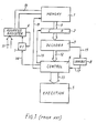
- FIG. 1 an information handling apparatus in the prior art is illustrated as a block diagram.
- a group of instructions which are used to program processing are preliminarily stored in a memory 1, in which a necessary instruction is designated by a content (an address) of an address register 6.
- To the memory 1 are coupled an address bus 10 and a data bus 9. These buses are respectively formed of a plurality of signal lines so as to be able to handle a plurality of bits simultaneously for executing a high-speed processing.
- An instruction designated by the content of the address register 6 is read out the memory 1 by a read-out control signal 18 from control circuit 4.
- an instruction code in the first byte thereof is fetched in an instruction register 2 in response to an instruction fetch signal 16 issued from a control circuit 4.
- This instruction code is decoded by a decoder 3, and the results are sent to the control circuit 4 via a bus 12.
- the control circuit 4 produces various kinds of control signals 13 and transmits them to an execution circuit 5 for processing a pragram, on the basis of the decoded results.
- the execution circuit 5 comprises element means used for executing a program such as registers, an arithmetic-logic unit, gate circuits, etc., and they execute a read-out instruction as controlled in timing by the control signals 13.
- the control circuit 4 applies an address advance signal 14 to an incrementer 7 in order to read out an instruction to be subsequently executed.
- the incrementer 7 has an addition facility for incrementing the present content in the address register 6 by +1 in response to the address advance signal 14.
- the address register 6 is programmable. Namely, any desired address can be set therein via a 6us 11 and its content can be reset.
- the address register 6 is programmable. Namely, any desired address can be set therein via a 6us 11 and its content can be reset.
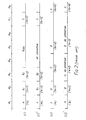
- reference symbols M 1 to M 8 denote successive machine cycles. While the machine cycles are normally allotted independently for the respective instructions, here for convenience of explanation, consecutive suffixes are added to the symbols M representing successive machine cycles. That is, description will be made here on instructions to be executed in the 8 machine cycles M 1 to M s . Depending upon an apparatus, the durations of machine cycles are different, but here it is assumed that all the machine cycles have the same duration. However it is to be noted that the present invention is will applicable to an apparatus having machine cycles of different durations. In Fig.
- A, B, C, D and E denote respective instructions, and parenthesized symbols n, n + 1, n + 2, n + 3 and n + 4 noted thereunder means addresses for designating the corresponding instruction. Furthermore, consecutive symbols 8 1 and B 2 indicate that the instruction B is a 2-byte instruction, and they denote the instruction codes of the first byte and the second byte, respectively.
- Fig. 2(i) shows the mode of operation in which for a 1-byte instruction A, a 2-byte instruction B and a 1-byte instruction C, processings inherently defined by the respective instructions are executed
- Fig. 2(i)' shows the mode of operation in which among the above-mentioned instructions, for the 2-byte instruction B the processing is made to be not executed
- Fig. 2(ii) shows the mode of operation in which the respective instructions are to be normally executed, in the case where all the instructions A to E are 1-byte instructions and among these instructions the instruction C and the instruction D, respectively, necessitate 2 machine cycles and 3 machine cycles
- Fig. 2(ii)' shows the mode of operation in the case where among the above-mentioned instructions the consecutive instructions C and D are made not to be executed.
- an address (n) is set in the address register 6, and thereby the instruction A is read out of the memory 1.
- the read instruction A is a 1-byte instruction, which is decoded by the decoder 3, and the decoded result is transmitted to the control circuit 4.
- the control circuit 4 On the basis of this decoded result, the control circuit 4 generates control signals 13 which are necessitated for execution of the instruction A, and in response to the control signals 13 processing is executed in the execution circuit 5. It is assumed that this processing can be executed in one machine cycle M i .
- the control circuit 4 When the execution of the instruction A has been finished (practically in the last state in the first machine cycle M i ), the control circuit 4 generates an address advance signal 14 for incrementing the content of the address register 6 by +1. As a result, the present content (n) of the address register 6 is modified to (n + 1) by the incrementer 7.
- the next machine cycle M 2 is a cycle allotted to the instruction B, and since the instruction B is a 2-byte instruction, in the machine cycle M 2 is read the instruction code B, of the first byte of the 2 bytes according to the modified address (n + 1). In this instruction code B, is set an information indicating that the instruction B is a 2- byte instruction.
- This procedure includes the processing for modifying the content of the address register 6 from (n + 1) to (n + 2) by controlling the incrementer 7. And in the next machine cycle M 3 is read the instruction code B 2 of the second byte. It is assumed that this instruction B necessitates 5 machine cycles in total before the processing designated by the instruction has been completely executed. Accordingly, the processing for the instruction B can be terminated at the end of the machine cycle M 6 . It is to be noted that during the machine cycles M 4 to M s , the content (n + 2) of the address register 6 is not modified.
- the two instruction codes B, and B 2 forming the 2-byte instruction B are read in the instruction register 3 during the machine cycles M 2 and M 3 , respectively, and they are decoded by the decoder 3.
- the inhibit circuit 8 is actuated to transmit an inhibit signal 17 to the control circuit 4, so that the control signals 13 in response to the instruction B may not be transmitted from the control circuit 4 to the execution circuit 5.
- the execution circuit 5 makes no operation during the period consisting of the machine cycles M 2 to M 6 which are normally necessitated for executing the instruction B.
- the execution circuit 5 makes no operation. In other words, a wasteful time is spent in the machine cycles M 2 to M e .
- the instructions A, B, C, D and E which are all one byte instructions, are executed, and among these instructions, the instructions C and D respectively necessitate 2 machine cycles and 3 machine cycles as a read-out and an execution periods. Accordingly, in the case where these instructions C and D are respectively inhibited from execution by the inhibit circuit 8 (Fig. 2(ii)'), the execution circuit 5 also wastefully spends a time without executing anything during the machine cycles M 3 to Me.
- addressing means for designating a next instruction is uniquely fixed so as to operate in response to machine cycles necessary to execute the present instruction.
- the apparatus is designed in such a manner that when the instruction not to be executed is formed of a plurality of bytes, all the bytes have to be read out of memory before shift to a next new instruction. Accordingly, the processing speed of the heretofore known apparatuses was, in any event, determined solely by the frequency of the operation clock applied to the apparatus and the procedure of processing a program, and it was impossible to further increase the processing speed.
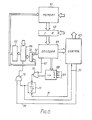
- FIG. 3 An information handling apparatus illustrating the principle employed in the present invention is shown in the block diagram of Fig. 3.
- a group of instructions, which are used for executing a program, are stored in a memory 21, and each memory location corresponding to instructions therein is designated by a content (address) of an address register 26. Then the designated instruction is read out of memory 21 in response to a read-out control signal 39.
- the read-out instruction is fetched into an instruction register 22.
- the address is transferred in a parallel form of a plurality of bits (for instance, 8 bits) through an address bus, and the instruction is read out in parallel form of a plurality of bits (for instance, 4 bits) through data bus 29.
- a fetch operation to the instruction register 22 is carried out in response to a fetch control signal 36 issued from a control circuit 24.
- the instruction set in the instruction register 22 is decoded by a decoder 23, and signals 32 representing the results of decoding are transferred to the control circuit 24.
- the control circuit 24 applies control signals 33, which are necessitated for executing the instruction, to a program execution circuit 25 on the basis of the decoded results.
- the execution circuit 25 executes the read-out instruction in response to the control signals 33.
- an instruction where execution should be canceled is handled.
- a signal 35 indicating that execution of the instruction should be inhibited is issued from the decoder 23, or a signal 38 indicating that execution of the instruction should be inhibited is issued from other circuit, such as an external peripheral unit or the like.
- an inhibited signal 37 is issued from an inhibit circuit 28, in response to the signal 35 or 35'.
- the inhibit signal 37 controls the control circuit 24 so that the control signals 33 on the basis of the decoded instruction may not be transferred from the control circuit 24 to the execution circuit 25.
- the instruction is nullified, and the execution circuit 25 does not execute the operation defined by the instruction.
- the execution circuit 25 either holds the previous condition or is reset.
- the decoder 23 applies information for advancing an address of the address register 26 to an address control circuit 27.
- this information 34 data representing how many bytes are included in the instruction to be nullified, could be used. This data is normally set in a first byte of the instruction which should be not executed, and therefore, the first byte of the instruction has to be read out of the memory 21 and to be decoded. For instance, if it is a 3-byte instruction, then information representing that the present content of the address register 26 (at this moment the content being the address designating the first byte of the instruction) would be advanced by 3, is applied to the address control circuit 27.
- the present invention is effective in the case where the instruction necessitates a plurality of machine cycles for execution. More particularly, the apparatus according to the present invention comprises means for modifying an address without respect to an execution of an instruction, and therefore, a processing for a next new instruction -can be immediately carried out after an address modification is terminated. The time period of this modification is at most one machine cycle. In this case, a reset signal 38 is applied to the inhibit circuit 28 after the modification is terminated.
- the inhibit condition of the execution circuit 25 is released, and so, a machine cycle succeeding to the machine cycle of the address modification can be effectively used as a read period for a next new instruction or an execution period for the read-out new instruction without being wasted as a non-execution period.
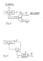
- Fig. 4 shows one example of the address control circuit employing an adder circuit 40, in which address advancing information 34 is applied to one input, and a present content 42 of the address register 26 is applied to the other input. The result of addition is once set in a register 41 and then transferred to the address register 26 as a new address. As a matter of course, the register 41 could be omitted and replaced by the address register 26.
- Fig. 5 shows another example of the address control circuit in which an incrementer 51 is used. From a register 52 which hold the present content of the address register 26, the content is input to the incrementer 51, and it is incremented by +1 each time when a signal 53 issued from a count control circuit 50.
- the count control circuit 50 detects the necessary number of counts on the basis of the address advance information 34 and thereby controls the incrementer 51.
- a signal 53 is a signal for instruction addition, and moreoever, since the addition can be executed at a high speed, it is possible to achieve the operations of addition a plurality of times within one machine cycle. In this connection it is preferable to synchronize the output timing of the signal 53 with a basic operation clock signal of the apparatus.
- a skip instruction This means such instruction that when a predetermined condition is fulfilled within a computer and/or external units added thereto, a processing is carried out such that an instruction stored at the memory location subsequent to the skip instruction is skipped (that is, the subsequent instruction is disregarded) and execution of the further subsequent instruction (the second instructions subsequent to the skip instruction) is commenced. For instance, it is assumed that a skip instruction reading "skip, if A - register is 0" and a branch or jump instruction reading "branch or jump to address X" subsequent to the skip instruction are stored consecutively in a memory.
- the skip instruction can achieve more widely such processing that the subsequent instructions are to be executed only when the condition designated by the skip instruction is not fulfilled, and the subsequent instructions are to be disregarded when the condition designated by the skip instruction is fulfilled.
- the same effect as this skip instruction can be achieved by employing the conventional conditional jump instruction and selecting the destination of jump at the second instruction subsequent to the conditional jump instruction.
- the skip instruction it is always necessary to designate the address of the jump location.
- the skip instruction has a merit that regardless of how many bytes the next instruction to be disregarded may comprise, the second instruction subsequent to the skip instruction can be used without designating the address of that instruction at all.
- the skip instruction is more excellent in view of effective utilization of a memory.
- the skip instructions for effecting such processing have been widely and conveniently utilized especially in a micro-computer of 4-bit system or 8-bit system or the like which has a fewer kinds of instructions.
- a processing of disregarding a certain instruction can be effectively utilized also in the following case.
- the processing enters this subroutine if it enters at the first instruction that the value "3" should be set in the A-register, then according to this subroutine at first 3 is set in the A-register, but since the next instruction, i.e., the instruction that the value "4" should be set in the A-register is an instruction of the same type as the aforementioned initially executed instruction that the value "3" should be set in the A-register (such instructions being defined to be of the same type), the above-mentioned next instruction is disregarded as a result of the above-referred function, and so, the processing proceeds further to the next subsequent instruction that the value "5" should be set in the A-register.
- the next instruction i.e., the instruction that the value "4" should be set in the A-register is an instruction of the same type as the aforementioned initially executed instruction that the value "3" should be set in the A-register (such instructions being defined to be of the same type)
- the above-mentioned next instruction is disregarded as a result of the
- this next subsequent instruction is disregarded because it is also of the same type as the preceding instruction, and after all, in this case, the subroutine would be executed by employing the value "3" initially set in the A-register as a parameter.
- the subroutine upon initially entering this subroutine, if the processing enters at the second instruction that the value "4" should be set in the A-register, then due to a similar processing to the above-described, in this case the subroutine would be executed by employing the value "4" as a parameter.
- the processing enters at the third instruction that the value "5" should be set in the A-register then the subroutine would be executed by employing the value 5 as a parameter.
- a microprogram control apparatus comprises a microprogram counter for designating a memory address of a micro-instruction, a decoder for determining whether or not a decoded micro-instruction belongs to a group of micro-instructions defined to be of the same type as the micro-instruction processed immediately before the decoded micro-instruction, means for suppressing execution of the decoded micro-instruction in the event that the micro-instruction decoded by said decoder has been determined to be of the same type as the micro-instruction processed immediately before the decoded micro-instruction, and means for setting the content of said microprogram counter so as to designate the address of the micro-instruction next to the decoded microprogram in the aforementioned event.
- FIG. 6 is a block diagram adapted for explaining the operation in response to a skip instruction.
- Reference numberal 61 designates a micro-instruction memory circuit.
- a first byte of this instruction stored at an address designated by an address counter 63 is read out of the memory 61. Then, it is stored in an instruction register 62.
- a decoder 64 controls a program counter control circuit 66.
- the content of the program counter 63 is stepped one by one, and thereby all the bytes belonging to that instruction are successively fetched in the instruction register 62 to be decoded. In this way, the processing designated by this decoded micro-instruction is executed by an execution circuit (not shown) that is controlled by the control circuit 65.
- the control circuit 65 further advances the content of the program counter 63 by 1 via the program counter control circuit 66. And in the next machine cycle, the first byte of the next instruction stored at the address designated by the content of this program counter 63 is read out, and thus the processing proceeds to execution of the next new instruction.
- a skip instruction has been fetched in the instruction register 62. As described above this is decoded by the instruction decoder 64, and due to the designation that this instruction is a skip instruction, a logic level on a skip instruction designating line 67 is turned to "1".
- the portion designating a skip condition in this skip instruction is fed to a skip condition selection circuit 68, in which among various skip conditional signals 69, a conditional signal designated by this skip condition is selected.
- these conditional signals 69 are included various conditional signals such as, for example, a signal adapted to take a logic level of "1" if the content of the aforementioned A-register is 0, but take a logic level of "0" if the content of the A-register is not 0, a signal adapted to take a logic level of "1” if input data are present at a designated into port but take a logic of "0” if input data are not present, or a signal indicating a detected condition of a carry output and/or a flag of an ALU.
- the conditional signal selected in the skip condition selection circuit 68 is combined with the signal on the above-mentioned skip instruction designating line 67 by means of an AND circuit 70, and applied to a set terminal of a flip-flop 71.
- the flip-flop 71 can be set provided that a skip instruction has been decoded and also that the condition designated by the skip instruction is fulfilled.
- the control circuit 65 controls the program counter control circuit 66 so as to advance the content of the program counter 63 by 1.
- the first byte of the instruction starting from the address next to this skip instruction is fetched in the instruction register 62. In this way, since information, of how many bytes a given instruction is formed, can be obtained by decoding the first byte of instruction, this information indicating a number of bytes of an instruction is entracted and applied to one input of an adder 73 via a byte number output line 72.
- this adder 73 To the other input of this adder 73 is applied the content of the program counter 63. Now, at the time point when the first byte of the instruction was read, the decoding of the number of bytes in that instruction was completed and also the addition of the input of the byte number and the content of the program counter 63 by means of the adder 73 has been completed in the above-described manner, the control circuit 65 outputs a program counter write pulse through a program counter write pulse line 74. This program counter write pulse line 74 and the output line of the above-mentioned flip-flop 71 are combined in logic by a second AND circuit 75.
- control circuit 65 generates a reset pulse at a time point near to the end of this machine cycle after it generated the write pulse on the program counter write pulse line 74.
- This reset pulse is applied to a reset terminal of the flip-flop 71 via a reset pulse line 76, and so, the flip-flop 71 is reset.
- the output of the flip-flop 71 is, in addition to serving as one input of the second AND circuit 75, applied via an instruction execution suppress signal line 77 to the control circuit 65 as an instruction execution suppress signal.
- the trailing edge portion of this suppress signal is utilized to set the control circuit 65 so that in the next machine cycle the byte fetched in the instruction register 62 may be processed as the first byte of the next new instruction.
- Fig. 7A represents the timing relation in the case of the prior art apparatus. Assuming that the memory address where a skip instruction is stored in n, initially when the content of the program counter is n, the skip instruction is read out. Here it is assumed that the skip condition is not fulfilled. Then, in the next machine cycle, the content of the program counter is incremented to n + 1, and the first byte of the next instruction is read out. It is assumed that this instruction is a 3-byte instruction (for instance, a call instruction) which necessitates 6 machine cycles for its execution.
- the timing chart in the case of the apparatus according to the present invention shown in Fig. 6, is illustrated in Fig. 7B.
- the mode of processing is quite similar to that in the case of the prior art apparatus shown in Fig. 7A.
- the program counter in the next one machine cycle subsequent to the skip instruction the program counter is advanced by the number of bytes of the instruction just subsequent to the skip instruction (the number of bytes of the instruction to be skipped) at a time.
- the program counter is advanced by 3 at a time.
- the processing can enter execution of the second instruction subsequent to the skip instruction.
- both the output of the flip-flop 71 and the output on the byte number output line 72 are directly applied to the program counter control circuit 66.
- the content of the program counter 63 could be stepped at a higher cycle repetition frequency than that employed in the regular instruction processing by a factor of the number of bytes designated by the output on the byte number output line 72.
- FIG. 8 A still another preferred embodiment of the present invention is illustrated in a block diagram in Fig. 8. While reference numeral 104 designates a decoder having a similar function to the instruction decoder 64 in Fig. 6, the former is further added with the following function. That is, when a first byte of a given instruction has been fetched in an instruction register 82, the decoder 104 compares the information contained in this newly read-out byte with the information contained in the first byte of the just preceding instruction which is stored in the decoder 104, to check whether or not the newly read-out instruction is of the same type in definition as the just preceding instruction. For this checking, it is only necessary to compare the respective instructions with respect to the principal portions of their codes or with respect to their code portions indicating the type of instructions.
- the decoder 104 outputs a pulse of logic level "1" onto a stack-up instruction detection line 107.
- This detection line 107 is coupled to a set terminal of a flip-flop 91, which has a similar function to the flip-flop 71 in Fig. 6, to set the flip-flop 91.
- the subsequent processing is almost similar to that described above with reference to Fig. 6, and in a program counter 83 is written an output of an adder 93 which operates to add the present content of the program counter 83 with an output on a byte number output line 92 which output represents the number of bytes of the decoded instruction.
- the set output of the flip-flop 91 controls a control circuit 85 via an instruction execution suppress signal line 97 so that execution of the decoded instruction may be suppressed.
- the above-mentioned processing is completed within the same machine cycle in which the first byte of this instruction was read out, similarly to the processing described above with reference to Fig. 6, and in the next subsequent machine cycle, the first byte of the next new instruction is read in the instruction register 82, so that the processing can immediately enter the machine cycle for executing the instruction.
- the output of the flip-flop 91 and the output on the byte number output line 92 could be directly applied to a program counter control circuit 86.
- the content of the program counter 83 could be stepped at a higher cycle repetition frequency than that employed in the regular instruction processing by a factor of the number of bytes designated by the output on the byte number output line 92.
Landscapes
- Engineering & Computer Science (AREA)
- Software Systems (AREA)
- Theoretical Computer Science (AREA)
- Physics & Mathematics (AREA)
- General Engineering & Computer Science (AREA)
- General Physics & Mathematics (AREA)
- Executing Machine-Instructions (AREA)
Claims (3)
Priority Applications (2)
| Application Number | Priority Date | Filing Date | Title |
|---|---|---|---|
| EP19810305553 EP0079995B1 (fr) | 1981-11-24 | 1981-11-24 | Appareil de traitement d'informations avec exécution d'instructions très rapide |
| DE8181305553T DE3174013D1 (en) | 1981-11-24 | 1981-11-24 | Information handling apparatus having an instruction-executing function at a high speed |
Applications Claiming Priority (1)
| Application Number | Priority Date | Filing Date | Title |
|---|---|---|---|
| EP19810305553 EP0079995B1 (fr) | 1981-11-24 | 1981-11-24 | Appareil de traitement d'informations avec exécution d'instructions très rapide |
Publications (2)
| Publication Number | Publication Date |
|---|---|
| EP0079995A1 EP0079995A1 (fr) | 1983-06-01 |
| EP0079995B1 true EP0079995B1 (fr) | 1986-03-05 |
Family
ID=8188463
Family Applications (1)
| Application Number | Title | Priority Date | Filing Date |
|---|---|---|---|
| EP19810305553 Expired EP0079995B1 (fr) | 1981-11-24 | 1981-11-24 | Appareil de traitement d'informations avec exécution d'instructions très rapide |
Country Status (2)
| Country | Link |
|---|---|
| EP (1) | EP0079995B1 (fr) |
| DE (1) | DE3174013D1 (fr) |
Families Citing this family (3)
| Publication number | Priority date | Publication date | Assignee | Title |
|---|---|---|---|---|
| EP1387255B1 (fr) | 2002-07-31 | 2020-04-08 | Texas Instruments Incorporated | Instruction de test et surpassement avec au moins un opérande de registre |
| EP1387254B1 (fr) * | 2002-07-31 | 2012-12-12 | Texas Instruments Incorporated | Instruction de surpassement réalisant un test avec des données directes |
| US11204768B2 (en) | 2019-11-06 | 2021-12-21 | Onnivation Llc | Instruction length based parallel instruction demarcator |
Family Cites Families (2)
| Publication number | Priority date | Publication date | Assignee | Title |
|---|---|---|---|---|
| US3408630A (en) * | 1966-03-25 | 1968-10-29 | Burroughs Corp | Digital computer having high speed branch operation |
| US3577190A (en) * | 1968-06-26 | 1971-05-04 | Ibm | Apparatus in a digital computer for allowing the skipping of predetermined instructions in a sequence of instructions, in response to the occurrence of certain conditions |
-
1981
- 1981-11-24 DE DE8181305553T patent/DE3174013D1/de not_active Expired
- 1981-11-24 EP EP19810305553 patent/EP0079995B1/fr not_active Expired
Also Published As
| Publication number | Publication date |
|---|---|
| EP0079995A1 (fr) | 1983-06-01 |
| DE3174013D1 (en) | 1986-04-10 |
Similar Documents
| Publication | Publication Date | Title |
|---|---|---|
| US4430706A (en) | Branch prediction apparatus and method for a data processing system | |
| US5235686A (en) | Computer system having mixed macrocode and microcode | |
| US5193157A (en) | Piplined system includes a selector for loading condition code either from first or second condition code registers to program counter | |
| US4323963A (en) | Hardware interpretive mode microprocessor | |
| EP0231928B1 (fr) | Circuit pour la commande par programme | |
| EP0124597B1 (fr) | Memoires multiples pour la commande dans micro-controleur a pipeline pour manipuler des sous-programmes de branchement et de retour a la sequence principale | |
| EP0045634A1 (fr) | Appareil de traitement de données digitales arrangé pour l'exécution d'instructions simultanées | |
| US4365311A (en) | Control of instruction pipeline in data processing system | |
| US20020078330A1 (en) | Computer system for executing branch instructions | |
| US4514804A (en) | Information handling apparatus having a high speed instruction-executing function | |
| US5504869A (en) | High speed processing system capable of executing strings of instructions in order without waiting completion of previous memory access instruction | |
| US4539635A (en) | Pipelined digital processor arranged for conditional operation | |
| EP0136183B1 (fr) | Dispositif de mémoire de commande pour le fonctionnement de pipeline d'un CPU | |
| US3408630A (en) | Digital computer having high speed branch operation | |
| EP0126125B1 (fr) | Memoires mutiples pour la commande d'un micro-controleur en pipeline | |
| EP0126124B1 (fr) | Memoires multiples pour la commande d'un micro-controleur a pipeline pour manipuler des sous-programmes emboites | |
| US20050149931A1 (en) | Multithread processor architecture for triggered thread switching without any cycle time loss, and without any switching program command | |
| US4093983A (en) | Fast and normal rate instruction fetching | |
| US5390306A (en) | Pipeline processing system and microprocessor using the system | |
| US20030028696A1 (en) | Low overhead interrupt | |
| EP0164418B1 (fr) | Systeme de commande par microprogramme | |
| EP0279953B1 (fr) | Ordinateur exécutant un mélange de micro- et macro-instructions | |
| US5621907A (en) | Microprocessor with memory storing instructions for time-compressed fetching of instruction data for a second cycle within a first machine cycle | |
| US5586337A (en) | Programmable controller with timing control | |
| US5479620A (en) | Control unit modifying micro instructions for one cycle execution |
Legal Events
| Date | Code | Title | Description |
|---|---|---|---|
| PUAI | Public reference made under article 153(3) epc to a published international application that has entered the european phase |
Free format text: ORIGINAL CODE: 0009012 |
|
| AK | Designated contracting states |
Designated state(s): DE FR GB |
|
| RAP1 | Party data changed (applicant data changed or rights of an application transferred) |
Owner name: NEC CORPORATION |
|
| 17P | Request for examination filed |
Effective date: 19830927 |
|
| GRAA | (expected) grant |
Free format text: ORIGINAL CODE: 0009210 |
|
| AK | Designated contracting states |
Kind code of ref document: B1 Designated state(s): DE FR GB |
|
| REF | Corresponds to: |
Ref document number: 3174013 Country of ref document: DE Date of ref document: 19860410 |
|
| ET | Fr: translation filed | ||
| PLBE | No opposition filed within time limit |
Free format text: ORIGINAL CODE: 0009261 |
|
| STAA | Information on the status of an ep patent application or granted ep patent |
Free format text: STATUS: NO OPPOSITION FILED WITHIN TIME LIMIT |
|
| 26N | No opposition filed | ||
| PGFP | Annual fee paid to national office [announced via postgrant information from national office to epo] |
Ref country code: FR Payment date: 19991109 Year of fee payment: 19 |
|
| PGFP | Annual fee paid to national office [announced via postgrant information from national office to epo] |
Ref country code: GB Payment date: 19991124 Year of fee payment: 19 |
|
| PGFP | Annual fee paid to national office [announced via postgrant information from national office to epo] |
Ref country code: DE Payment date: 19991129 Year of fee payment: 19 |
|
| PG25 | Lapsed in a contracting state [announced via postgrant information from national office to epo] |
Ref country code: GB Free format text: LAPSE BECAUSE OF NON-PAYMENT OF DUE FEES Effective date: 20001124 |
|
| GBPC | Gb: european patent ceased through non-payment of renewal fee |
Effective date: 20001124 |
|
| PG25 | Lapsed in a contracting state [announced via postgrant information from national office to epo] |
Ref country code: FR Free format text: LAPSE BECAUSE OF NON-PAYMENT OF DUE FEES Effective date: 20010731 |
|
| PG25 | Lapsed in a contracting state [announced via postgrant information from national office to epo] |
Ref country code: DE Free format text: LAPSE BECAUSE OF NON-PAYMENT OF DUE FEES Effective date: 20010801 |
|
| REG | Reference to a national code |
Ref country code: FR Ref legal event code: ST |