EP0080936A2 - Dispositif de mémoire semi-conductrice dynamique - Google Patents
Dispositif de mémoire semi-conductrice dynamique Download PDFInfo
- Publication number
- EP0080936A2 EP0080936A2 EP82402139A EP82402139A EP0080936A2 EP 0080936 A2 EP0080936 A2 EP 0080936A2 EP 82402139 A EP82402139 A EP 82402139A EP 82402139 A EP82402139 A EP 82402139A EP 0080936 A2 EP0080936 A2 EP 0080936A2
- Authority
- EP
- European Patent Office
- Prior art keywords
- level
- bit line
- transistors
- transistor
- sense amplifier
- Prior art date
- Legal status (The legal status is an assumption and is not a legal conclusion. Google has not performed a legal analysis and makes no representation as to the accuracy of the status listed.)
- Granted
Links
Images


Classifications
-
- G—PHYSICS
- G11—INFORMATION STORAGE
- G11C—STATIC STORES
- G11C11/00—Digital stores characterised by the use of particular electric or magnetic storage elements; Storage elements therefor
- G11C11/21—Digital stores characterised by the use of particular electric or magnetic storage elements; Storage elements therefor using electric elements
- G11C11/34—Digital stores characterised by the use of particular electric or magnetic storage elements; Storage elements therefor using electric elements using semiconductor devices
- G11C11/40—Digital stores characterised by the use of particular electric or magnetic storage elements; Storage elements therefor using electric elements using semiconductor devices using transistors
- G11C11/401—Digital stores characterised by the use of particular electric or magnetic storage elements; Storage elements therefor using electric elements using semiconductor devices using transistors forming cells needing refreshing or charge regeneration, i.e. dynamic cells
- G11C11/4063—Auxiliary circuits, e.g. for addressing, decoding, driving, writing, sensing or timing
- G11C11/407—Auxiliary circuits, e.g. for addressing, decoding, driving, writing, sensing or timing for memory cells of the field-effect type
- G11C11/409—Read-write [R-W] circuits
- G11C11/4091—Sense or sense/refresh amplifiers, or associated sense circuitry, e.g. for coupled bit-line precharging, equalising or isolating
Definitions
- the present invention relates to a dynamic semiconductor memory device provided with an active restore circuit in which, in reading out data from a memory cell, the bit line voltage is not adversely influenced by the readout operation.
- a selected cell is connected to one of a pair of bit lines connected to a sense amplifier and a dummy cell is connected to the other bit line so as to perform a readout operation. Further, an active restor circuit is connected to the pair of bit lines so that the bit line voltage is not adversely influenced by the readout operation.
- an active restore circuit of the above-mentioned type can ensure the detection of information in the memory cell by pulling up the bit line on the high potential side of the electric source to a power source voltage Vcc just after actuation of the sense amplifier.
- the sense amplifier sometimes cannot definitely distinguish the potential difference between the two bit lines, and, as a result, an error occurs in reading out the stored information.
- An object of the present invention is to provide a dynamic semiconductor memory device having an active restore circuit in which information is accurately read out of a memory cell.
- Another object of the present invention is to provide a dynamic semiconductor memory device having an active restore circuit in which charges other than the necessary charges are not supplied to the bit lines.
- a dynamic semiconductor memory device comprising: a selected real cell connected to a word line and to one of a pair of bit lines connected to a sense amplifier; a dummy cell connected to another word line and to the other bit line; and an active restore circuit which is formed from bit line pull-up transistors, each of which is connected between one of the bit lines and a high potential source level, and a control signal is supplied to each of said bit line pull-up transistors after actuation of the sense amplifier, each of the bit line pull-up transistors being turned on so that the bit lines are pulled up to the high potential source level, the level of the control signal being maintained at a voltage potential level lower than the ground level from the time of actuation of the word line to the time of actuation of said sense amplifier.
- a conventional dynamic semiconductor memory device having an active restore circuit has the structure shown in Fig. 1.
- reference numerals 1 and 2 each represent a memory cell
- reference numeral 3 represents an active restore circuit
- reference numerals 5 and 6 each represent a dummy cell
- reference numeral 7 represents a power source line
- reference numeral 8 represents a sense amplifier
- reference numeral 9 represents a metal-oxide semiconductor (MOS) capacitor
- reference numeral 12 represents a bit line pull-up transistor.
- the symbols BL and BL each represent a bit line
- the symbol WL represents a word line
- the symbol DWL represents a dummy word line
- the symbols WLS and DWLS represent a selected word line and a selected dummy word line, respectively.
- a clock pulse signal ⁇ O put into an operation control input 4 is set at a high level and transistors Q3 and Q4 are turned on to pre-charge nodes N1 and N2 to a high level. Furthermore, transistors Q10 and Qll are turned on by the clock pulse signal ⁇ O to pre-charge the bit lines BL and BL.
- the word line WLS and the dummy word line DWLS are set at a high level, and the information stored in the memory cell 1 is read out of the memory cell 1. Since the potential of the bit line BL is changed according to the distribution of charges between the bit line BL and the memory cell 1, the potential of the bit line BL is changed according to the distribution of charged between the bit line BL and the dummy cell 6. When the information of the memory cell 1 is "O”, the potential of the bit line BL is reduced to below the potential of the bit line BL. Then a clock signal ⁇ l is set at a high level to actuate the sense amplifier 8.
- a clock pulse signal ⁇ 2 supplied to a terminal 10 is raised up, and by capacitive coupling, the potential of the node N2 is set at a level higher than Vcc to turn on a bit line pull-up transistor Q2 and to raise up the potential of the bit line BL to Vcc, whereby detection of the information in the memory cell is definitely accomplished.
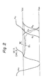
- the word line WLS is driven and the memory cell 1 is selected, and although the potential of the bit line BL will drop, since the nodes N1 and N2 are pre-charged at a high potential level, if the potential of the bit line BL drops and the voltage between the gate and source of the transistor Ql exceeds the threshold voltage Vth of the transistor Ql, the transistor Ql is turned on and a charge is supplied to the bit line BL from the power source line 7 to inhibit dropping of the voltage of the bit line BL, with the result that the difference in voltage between the bit lines BL and BL is diminished (see Fig. 2).
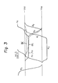
- the specific circuit structure of the embodiment of the present invention is substantially the same as the structure of the conventional circuit shown in Fig. 1 except that, as shown in Fig. 3, the potential of the clock pulse signal ⁇ 2 supplied to the input terminal 10 of the MOS capacitor 9 is set at a level lower than the level of the ground potential Vss during the period from the time of actuation of the word line WLS of the dynamic memory cell and the dummy word line DWLS of the dummy cell to the time of actuation of the sense amplifier 8, that is, the time of rising of the clock pulse signal ⁇ l supplied to an operation control input 11, so that the active restore circuit 3 is not operated, that is, the transistors Ql and Q2 are not turned on.
- a circuit generating this clock pulse signal ⁇ 2 is shown in Fig. 4.
- This circuit comprises transistors Q6 and Q7 connected in series to each other between power source lines l1 and l2, transistors Q8 and Q9 connected in series to each other and being parallel to the transistors Q6 and Q7, and a capacitor C connected between node N4, located between the transistors Q6 and Q7, and a node N3, located between the transistors Q8 and Q9.
- a voltage generated at the node N4 is taken out as the clock pulse signal ⁇ 2.
- Signals ⁇ 3 through ⁇ 6 having the voltage waveforms shown in Fig. 5 are supplied to gate inputs 12 through 15 of the transistors Q6 through Q9, respectively.
- the clock pulse signal ⁇ 2 is first described.
- the clock pulse signals ⁇ 4 and ⁇ 5 are put into the gate inputs 13 and 14 of the circuit so as set them at a high level, the transistors Q7 and Q8 are turned on, the node N4 is maintained at the voltage Vss (ground voltage level), and the node N3 is maintained at the voltage (Vcc - Vth), in which Vth represents the threshold voltage of the transistor Q8 and Vcc represents the voltage of the power source line l1.
- the clock pulse signals ⁇ 4 and ⁇ 5 are set at a low level, that is, at the ground voltage Vss, so as to turn off the transistors Q7 and Q8.
- the clock pulse signal Q6 supplied to the gate input 15 of the transistor 9 is maintained at a high level so as to set the node N3 at the voltage Vss. Accordingly, due to the capacitive coupling of the capacitor C, the voltage of the node N4 is set at a level (52 in Fig. 5) lower than the level of the ground voltage Vss.
- the clock pulse signal ⁇ 2 which is lower than Vss, is supplied to the input terminal 10 of the MOS capacitor 9 during the period from the time of actuation of the word line WLS to the time of actuation of the sense amplifier (the rising of the clock signal ⁇ l).
- This voltage causes the potentials of the nodes Nl and N2 to drop, with the result that operation of the bit line pull-up transistors 12 of the active restore circuit 3 is not effected. Accordingly, dropping of the voltage of the bit line BL is increased, and the difference between the potential of the bit line BL and the potential of the bit line BL is definitely detected by the sense amplifier. In the conventional circuit, this potential difference is diminished, and, as a result, an error is often made in reading out stored information. According to the present invention, however, this error can effectively be prevented.
- the control signals ⁇ 3 , ⁇ 4 , ⁇ 5 , and ⁇ 6 in Fi g . 4 , the word line drive signals WLS and DWLS, and the clock pulse signals ⁇ 0 , ⁇ 1 , and ⁇ 2 are generated by the circuit shown in Fig. 6.
- ⁇ 6 generator 21 is connected to WLS, DWLS generator 22 and, further, to ⁇ 1 generator 23, which generator 23 resets the output of the ⁇ 6 generator 21.
- the output of the ⁇ 1 generator 23 is connected to the ⁇ 5 generator 24, which is actuated due to a time delay and reset by the rising portion of the output of the ⁇ 6 generator 21.
- the output of ⁇ 0 , ⁇ 4 generator 25 is also reset by the rising portion of the output of the ⁇ 6 generator 21.
- the output of the ⁇ 1 generator 23 is connected to the 0 3 generator 26, which is actuated due to a time delay and which generates an output having a value higher than the source voltage Vcc.
- the output of the ⁇ 3 generator 26 is connected to the ⁇ 2 generator 27, which generates the clock pulse signal ⁇ 2 due to a time delay at the output of the ⁇ 3 generator 26.
- the active restore circuit is not actuated during the period from the time of actuation of the word line to the time of actuation of the sense amplifier even if the voltage of the bit line is dropped due to the reading out of stored information.
- the potential difference between the bit lines can definitely be detected. Therefore, the problem which often occurs in the conventional circuit, that is, the erroneous reading out of stored information, can be effectively prevented.
Landscapes
- Engineering & Computer Science (AREA)
- Microelectronics & Electronic Packaging (AREA)
- Computer Hardware Design (AREA)
- Dram (AREA)
- Semiconductor Memories (AREA)
Applications Claiming Priority (2)
| Application Number | Priority Date | Filing Date | Title |
|---|---|---|---|
| JP56190370A JPS5894189A (ja) | 1981-11-27 | 1981-11-27 | ダイナミツク型半導体記憶装置 |
| JP190370/81 | 1981-11-27 |
Publications (3)
| Publication Number | Publication Date |
|---|---|
| EP0080936A2 true EP0080936A2 (fr) | 1983-06-08 |
| EP0080936A3 EP0080936A3 (en) | 1985-11-06 |
| EP0080936B1 EP0080936B1 (fr) | 1988-08-03 |
Family
ID=16257044
Family Applications (1)
| Application Number | Title | Priority Date | Filing Date |
|---|---|---|---|
| EP82402139A Expired EP0080936B1 (fr) | 1981-11-27 | 1982-11-24 | Dispositif de mémoire semi-conductrice dynamique |
Country Status (4)
| Country | Link |
|---|---|
| US (1) | US4481610A (fr) |
| EP (1) | EP0080936B1 (fr) |
| JP (1) | JPS5894189A (fr) |
| DE (1) | DE3278866D1 (fr) |
Cited By (1)
| Publication number | Priority date | Publication date | Assignee | Title |
|---|---|---|---|---|
| EP0168246A3 (en) * | 1984-07-10 | 1988-04-27 | Nec Corporation | Improved active pull-up circuit |
Families Citing this family (5)
| Publication number | Priority date | Publication date | Assignee | Title |
|---|---|---|---|---|
| JPS59132492A (ja) * | 1982-12-22 | 1984-07-30 | Fujitsu Ltd | 半導体記憶装置 |
| US5122914A (en) * | 1984-01-17 | 1992-06-16 | Norand Corporation | Disk drive system with transportable carrier and mounting assembly |
| JPH0612612B2 (ja) * | 1987-03-06 | 1994-02-16 | 株式会社東芝 | 半導体記憶装置 |
| JPH0715952B2 (ja) * | 1988-04-13 | 1995-02-22 | 株式会社東芝 | 半導体記憶装置 |
| US5270967A (en) * | 1991-01-16 | 1993-12-14 | National Semiconductor Corporation | Refreshing ferroelectric capacitors |
Family Cites Families (3)
| Publication number | Priority date | Publication date | Assignee | Title |
|---|---|---|---|---|
| GB1576970A (en) * | 1977-12-22 | 1980-10-15 | Signetics Corp | Sense and refresh amplifier |
| US4363111A (en) * | 1980-10-06 | 1982-12-07 | Heightley John D | Dummy cell arrangement for an MOS memory |
| JPS57109187A (en) * | 1980-12-25 | 1982-07-07 | Mitsubishi Electric Corp | Re-charging circuit |
-
1981
- 1981-11-27 JP JP56190370A patent/JPS5894189A/ja active Granted
-
1982
- 1982-11-24 DE DE8282402139T patent/DE3278866D1/de not_active Expired
- 1982-11-24 US US06/444,487 patent/US4481610A/en not_active Expired - Fee Related
- 1982-11-24 EP EP82402139A patent/EP0080936B1/fr not_active Expired
Cited By (1)
| Publication number | Priority date | Publication date | Assignee | Title |
|---|---|---|---|---|
| EP0168246A3 (en) * | 1984-07-10 | 1988-04-27 | Nec Corporation | Improved active pull-up circuit |
Also Published As
| Publication number | Publication date |
|---|---|
| JPH0217872B2 (fr) | 1990-04-23 |
| EP0080936A3 (en) | 1985-11-06 |
| JPS5894189A (ja) | 1983-06-04 |
| EP0080936B1 (fr) | 1988-08-03 |
| DE3278866D1 (en) | 1988-09-08 |
| US4481610A (en) | 1984-11-06 |
Similar Documents
| Publication | Publication Date | Title |
|---|---|---|
| EP0473360B1 (fr) | Dispositif de mémoire à semi-conducteurs | |
| US4601017A (en) | Semiconductor memory device having active pull-up circuits | |
| EP0217601A2 (fr) | Cellule de mémoire | |
| EP0643393A2 (fr) | Dispositif de mémoire à semi-conducteurs avec circuit élévateur de tension | |
| JPH0462436B2 (fr) | ||
| EP0045215A2 (fr) | Circuit actif de remontée | |
| US4397003A (en) | Dynamic random access memory | |
| EP0233453A1 (fr) | Elément de mémoire associative | |
| US4338679A (en) | Row driver circuit for semiconductor memory | |
| KR910000383B1 (ko) | 다이나믹형 랜덤억세스메모리 | |
| US4336465A (en) | Reset circuit | |
| KR0139496B1 (ko) | 반도체 메모리장치의 비트라인 감지증폭기 | |
| EP0080936B1 (fr) | Dispositif de mémoire semi-conductrice dynamique | |
| KR950014256B1 (ko) | 낮은 전원전압을 사용하는 반도체 메모리장치 | |
| US5777934A (en) | Semiconductor memory device with variable plate voltage generator | |
| US5267192A (en) | Semiconductor memory device | |
| EP0040001B1 (fr) | Dispositif de mémoire dynamique à semi-conducteurs à chronologie réduite | |
| JPH09185886A (ja) | データ保持回路 | |
| US5539701A (en) | Sense circuit for semiconductor memory devices | |
| US6002624A (en) | Semiconductor memory device with input/output masking function without destruction of data bit | |
| US6249462B1 (en) | Data output circuit that can drive output data speedily and semiconductor memory device including such a data output circuit | |
| US5703819A (en) | Sense amplifier driving circuit | |
| EP0212946B1 (fr) | Dispositif de mémoire semi-conductrice | |
| EP0318094B1 (fr) | Circuit de mémorisation intégré à réglage interne de la tension d'alimentation | |
| KR100264213B1 (ko) | 반도체 메모리의 센스앰프 |
Legal Events
| Date | Code | Title | Description |
|---|---|---|---|
| PUAI | Public reference made under article 153(3) epc to a published international application that has entered the european phase |
Free format text: ORIGINAL CODE: 0009012 |
|
| AK | Designated contracting states |
Designated state(s): DE FR GB |
|
| PUAL | Search report despatched |
Free format text: ORIGINAL CODE: 0009013 |
|
| AK | Designated contracting states |
Designated state(s): DE FR GB |
|
| 17P | Request for examination filed |
Effective date: 19860424 |
|
| 17Q | First examination report despatched |
Effective date: 19870707 |
|
| GRAA | (expected) grant |
Free format text: ORIGINAL CODE: 0009210 |
|
| AK | Designated contracting states |
Kind code of ref document: B1 Designated state(s): DE FR GB |
|
| REF | Corresponds to: |
Ref document number: 3278866 Country of ref document: DE Date of ref document: 19880908 |
|
| ET | Fr: translation filed | ||
| PLBE | No opposition filed within time limit |
Free format text: ORIGINAL CODE: 0009261 |
|
| STAA | Information on the status of an ep patent application or granted ep patent |
Free format text: STATUS: NO OPPOSITION FILED WITHIN TIME LIMIT |
|
| 26N | No opposition filed | ||
| PGFP | Annual fee paid to national office [announced via postgrant information from national office to epo] |
Ref country code: GB Payment date: 19920903 Year of fee payment: 11 |
|
| PGFP | Annual fee paid to national office [announced via postgrant information from national office to epo] |
Ref country code: FR Payment date: 19921127 Year of fee payment: 11 |
|
| PGFP | Annual fee paid to national office [announced via postgrant information from national office to epo] |
Ref country code: DE Payment date: 19930129 Year of fee payment: 11 |
|
| PG25 | Lapsed in a contracting state [announced via postgrant information from national office to epo] |
Ref country code: GB Effective date: 19931124 |
|
| GBPC | Gb: european patent ceased through non-payment of renewal fee |
Effective date: 19931124 |
|
| PG25 | Lapsed in a contracting state [announced via postgrant information from national office to epo] |
Ref country code: FR Effective date: 19940729 |
|
| PG25 | Lapsed in a contracting state [announced via postgrant information from national office to epo] |
Ref country code: DE Effective date: 19940802 |
|
| REG | Reference to a national code |
Ref country code: FR Ref legal event code: ST |