EP0081052A2 - Additionneur complet et circuit d'opération comportant une pluralité d'additionneurs complets - Google Patents
Additionneur complet et circuit d'opération comportant une pluralité d'additionneurs complets Download PDFInfo
- Publication number
- EP0081052A2 EP0081052A2 EP82108974A EP82108974A EP0081052A2 EP 0081052 A2 EP0081052 A2 EP 0081052A2 EP 82108974 A EP82108974 A EP 82108974A EP 82108974 A EP82108974 A EP 82108974A EP 0081052 A2 EP0081052 A2 EP 0081052A2
- Authority
- EP
- European Patent Office
- Prior art keywords
- signal
- output signal
- input
- output
- selecting means
- Prior art date
- Legal status (The legal status is an assumption and is not a legal conclusion. Google has not performed a legal analysis and makes no representation as to the accuracy of the status listed.)
- Granted
Links
Images



Classifications
-
- G—PHYSICS
- G06—COMPUTING OR CALCULATING; COUNTING
- G06F—ELECTRIC DIGITAL DATA PROCESSING
- G06F7/00—Methods or arrangements for processing data by operating upon the order or content of the data handled
- G06F7/38—Methods or arrangements for performing computations using exclusively denominational number representation, e.g. using binary, ternary, decimal representation
- G06F7/48—Methods or arrangements for performing computations using exclusively denominational number representation, e.g. using binary, ternary, decimal representation using non-contact-making devices, e.g. tube, solid state device; using unspecified devices
- G06F7/50—Adding; Subtracting
- G06F7/501—Half or full adders, i.e. basic adder cells for one denomination
- G06F7/5016—Half or full adders, i.e. basic adder cells for one denomination forming at least one of the output signals directly from the minterms of the input signals, i.e. with a minimum number of gate levels
Definitions
- the present invention relates to a full adder applied to an operation circuit or the like.
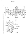
- Fig. 1 shows a conventional full adder which is composed of complementary MOSFETs. This full adder is described on PP. 51-54 of Proceedings of the conference on Solid State Devices, Tokyo, 1981; JJAP, vol. 21 (1981) Supplement 21-1.
- the full adder has p-channel MOSFETs Pl to P14 and n-channel MOSFETs N1 to N14.
- Reference symbols X0, YO and ZO denote input signals; C0, a carry output signal; S0, a sum output signal.
- the carry output signal C0 and the sum output signal SO are given by the following relations:
- the conventional full adder with the arrangement shown in Fig. 1 has a disadvantage in that the number of elements is increased since 28 MOSFETs are used. Therefore, the chip size is increased when an adder is integrated.
- an object of the present invention to provide a full adder which is suitable for adopting complementary MOSFETs and which requires only a small number of elements.
- a full adder comprising: a first logic circuit having an inverter which receives a first input signal and a first selector circuit which receives the first input signal and an output signal from said first inverter and which selectively produces one of the first input signal and the output signal from said first inverter in response to a second input signal; a second logic circuit having a second inverter which receives an output signal from said first selector circuit and a second selector circuit which receives the output signal from said first selector circuit and an output signal from said second inverter and which selectively produces one of the output signal from said first selector circuit and the output signal from said second inverter in response to a third input signal; and a third logic circuit which receives a signal corresponding to the first input signal and a signal corresponding to the output signal from said second selector circuit and which selectively produces one of the signal corresponding to the first input signal and the signal corresponding to the output signal from said second selector circuit.
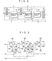
- Fig. 2 shows a full.adder according to a first embodiment of the present invention.
- Reference numeral X denotes a first input signal; Y, a second input signal; Z, a third input signal; S, a sum output signal of an operation result; and C, a carry output signal of the operation result.
- the first and second input signals X and Y are supplied to a logic circuit 1.
- the logic circuit 1 has an inverter 11 and a selector circuit 12.
- the inverter 11 receives the first input signal X and produces a signal H.
- the output signal H is supplied to the first input terminal of the selector circuit 12.
- the first input signal X is supplied to the second input terminal of the selector circuit 12.
- the second input signal Y is supplied to the third input terminal of the selector circuit 12.
- the selector circuit 12 selects one of the output signal H from the inverter 11 and the first input signal X and produces it in response to the logical level of the second input signal Y.
- An output signal J from the selector circuit 12 and the third input signal Z are supplied to a logic circuit 2.
- the logic circuit 2 has an inverter 13 and a selector circuit 14.
- the inverter 13 receives the output signal J and produces an output signal K.
- the output signal K is supplied to the first input terminal of the selector circuit 14.
- the output signal J from the inverter 12 is supplied to the second input terminal of the selector circuit 14.
- the third input signal Z is supplied to the third input terminal of the selector circuit 14.
- the selector circuit 14 selects one of the output signal K from the inverter 13 and the output signal J from the selector circuit 12 and produces it in response to the logical level of the third input signal Z.
- the output signal S from the selector circuit 14, the output signal H from the inverter 11, and the output signal K from the inverter 13 are supplied to a logic circuit 3.
- the logic circuit 3 has a selector circuit 15 and an inverter 16.
- the output signal S from the selector circuit 14 is supplied to the first input terminal of the selector circuit 15.
- the output signal H from the inverter 11 is supplied to the second input terminal of the selector circuit 15.
- the selector circuit 15 selects one of the output signal S and the output signal H and produces it in response to the logical level of the output signal K.
- the inverter 16 receives an output signal L from the selector circuit 15 and produces an output signal C.
- the selector circuit 12 uses as the selection control signal the second input signal Y.
- the selector circuit 12 selects an inverted signal of the first input signal X, that is, the output signal H from the inverter 11 when the second input signal Y is high.
- the selector signal 12 selects the first input signal X when the output signal Y is low.
- the selected one of the signals is produced as the output signal J.
- the logical level of the output signal J obtained in accordance with a combination of the logical levels of the input signals X and Y is shown in Table 1 below.
- the selector circuit 14 uses as the selection control signal the third input signal Z.
- the selector circuit 14 selects an inverted signal of the output signal J, that is, the output signal K from the inverter 13 when the third input signal Z is high.
- the selector circuit 14 selects the output signal J when the third input signal Z is low.
- the selected one of the signals is produced as the sum output signal S.
- the logical levels of the sum output signal S obtained in accordance with a combination of the logical levels of the output signal J and the third input signal Z are shown in Table 2 below.
- the selector circuit 15 uses as the selection control signal the output signal K from the inverter 13.
- the selector circuit 15 selects an inverted signal of the first input signal X, that is, the output signal H from the inverter 11, when the output signal K is high.
- the selector circuit 15 selects the sum output signal S from the selector circuit 14, when the output signal K is low.
- the selected one of the signals is produced as the output signal L.
- the output signal L is inverted by the inverter 16 and is produced as the carry output signal C. Therefore, in this case, the logical levels of the output signal L and the carry output signal C obtained in accordance with a combination of the logical levels of the signal K and the first input signal X are shown in Table 3 below.
- the signal S is the inverted signal of the signal S.
- the signal S is produced as the sum output signal in response to the first, second and third input signals X, Y and Z.
- the signal C is produced as the carry output signal in response to the signals X, Y and Z.
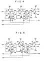
- Fig. 3 shows a circuit in which complementary MOSFETs are used to obtain the full adder shown in Fig. 2.
- Signals Xl, Yl, Zl, Hl, Jl, Kl, Ll, Sl and Cl in Fig. 3 correspond to the signals X, Y, Z, H, J, K, L, S and C respectively.
- the inverter 11 is constituted by a CMOS inverter which comprises a p-channel MOSFET TP1 and an n-channel MOSFET TN1.
- the selector circuit 12 is constituted by an n-channel MOSFET TN2 and a p-channel MOSFET TP2 whose output terminals are connected to each other.
- the output signal Hl from the inverter 11 is supplied to the free end, that is, the input terminal of the n-channel MOSFET TN2.
- the input signal Xl is supplied to the free end, that is, the input terminal of the p-channel MOSFET TP2.
- the input signal Yl is supplied as the selection control signal to the gates of the n- and p-channel MOSFETS TN2 and TP2.
- the output signal J1 is produced at the common node of the output terminal of the n- and p-channel MOSFETs TN2 and T P 2.
- the inverter 13 is constituted by a CMOS inverter which comprises a p-channel MOSFET TP3 and an n-channel MOSFET TN3.
- the selector circuit 14 is constituted by an n-channel MOSFET TN4 and a p-channel MOSFET TP4 whose output terminals are connected to each other.
- the output signal Kl is supplied to the free end, that is, the input terminal of the n-channel MOSFET TN4.
- the output signal Jl is supplied to the free end, that is, the input terminal of the p-channel MOSFET TP4.
- the third input signal Zl is supplied as the selection control signal to the gates of the n- and p-channel MOSFETs TN4 and TP4.
- the output signal Sl is produced at the common node of the output terminals of the n- and p-channel MOSFETs TN4 and TP4.
- the selector circuit 15 is constituted by a p-channel MOSFET TP5 and an n-channel MOSFET TN5 whose output terminals are connected to each other.
- the output signal Sl from the selector circuit 14 is supplied to the" free end, that is, the input terminal of the p-channel MOSFET TP5.
- the output signal Hl from the inverter 11 is supplied to the free end, that is, the input terminal of the n-channel MOSFET TN5.
- the output signal Kl from the inverter 13 is supplied as the selection control signal to the gates of the p- and n-channel MOSFETs TP5 and TN5.
- the output signal Ll is produced at the common node of the output terminals of the'p- and n-channel MOSFETs TP5 and TN5.
- the inverter 16 is constituted by a CMOS inverter which comprises a p-channel MOSFET TP6 and an n-channel MOSFET TN6.
- the n-channel MOSFET TN2 is ON when the second input signal Yl is high.
- the inverted signal Hl of the first input signal Xl is produced as the output signal Jl by the selector circuit 12.
- the p-channel MOSFET TP2 is ON when the second input signal Yl is low.
- the selector circuit 12 selectively produces the first input signal Xl. Therefore, the circuit arrangement using the n- and p-channel MOSFETs TN2 and TP2 is equivalent to the selector circuit 12 shown in Fig. 2.
- the n-channel MOSFET TN4 is ON when the third input signal Zl is high.
- the selector circuit 14 selectively produces the inverted signal Kl of the output signal Jl.
- the p-channel MOSFET TP4 is ON when the third input signal Zl is low.
- the selector circuit 14 selectively produces the signal Jl. Therefore, the circuit arrangement using the n- and p-channel MOSFETs TN4 and TP4 is equivalent to the selector circuit 14 shown in Fig. 2.
- the p-channel MOSFET TP5 is ON when the signal Kl is low.
- the selector circuit 15 then selectively produces the sum output signal Sl.
- the n-channel MOSFET TN5 is ON when the signal Kl is high.
- the selector circuit 15 then selectively produces the inverted signal Hl of the first input signal Xl. Therefore, the circuit arrangement using the p- and n-channel MOSFETs TP5 and TN5 is equivalent to the selector circuit 15 shown in Fi g . 2.
- the circuit shown in Fig. 3 performs the function of the full adder shown in Fig. 2.
- a total of only 12 MOSFETs are used.
- the number of elements is greatly decreased as compared with the conventional MOSFET adder. Therefore, the chip area of the full adder can be made compact when it is integrated.
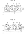
- Fig. 4 shows another example of a circuit in which the complementary MOSFETs are used to obtain the full adder shown in Fig. 2.
- Signals X2, Y2, Z2, H2, J2, K2, L2, S2 and C2 in Fig. 4 correspond to the signals X, Y, Z, H, J, K, L, S and C respectively.
- the circuit shown in Fig. 4 is the same as that in Fig. 3 except that selector circuits 12, 14 and 15 are connected in a different manner.
- the signal selection function based on the selection control signals is opposite to that shown in Fig. 3.
- the selector circuit 12 is constituted by a p-channel MOSFET TP7 and an n-channel MOSFET TN7 whose output terminals are connected to each other.
- the output signal H2 from the inverter 11 is supplied to the free end, that is, the input terminal of the p-channel M OSFET TP7.
- the first input signal X2 is supplied to the free end, that is, the input terminal of the n-channel MO SFET TN7.
- the second input signal Y2 is supplied as the selection control signal to the gates of the n- and p-channel MOSFETs TN7 and TP7.
- the signal J2 is produced at the common node of the output terminals of the p- and n-channel MOSFETS TP7 and TN7.
- the selector circuit 14 is constituted by a p-channel MOSFET TP8 and an n-channel MOSFET TN8 whose output terminals are connected to each other.
- the output signal K2 from the inverter 13 is supplied to the free end, that is, the input terminal of the MOSFET TP8.
- the output signal J2 from the selector circuit 12 is supplied to the free end, that is, the input terminal of the n-channel MOSFET TN8.
- the third input signal Z2 is supplied as the selection control signal to the gates of the p- and n-channel MOSFETs TP8 and TN8.
- the signal S2 is produced at the common node of the output terminals of the p- and n-channel MOSFETs TP8 and TN8.
- the selector circuit 15 is constituted by an n-channel MOSFET TN9 and a p-channel MOSFET TP9 whose output terminals are connected to each other.
- the output signal S2 from the selector circuit 14 is supplied to the free end, that is, the input terminal of the MOSFET TN9.
- the output signal H2 from the inverter 11 is supplied to the free end, that is, the input terminal of the p-channel MOSFET TP9.
- the output signal K2 from the inverter 13 is supplied as the selection control signal to the gates of the n- and p-channel MOSFETs TN9 and TP9.
- the signal L2 is produced at the common node of the output terminals of the n- and p-channel MOSFETs TN9 and TP9.
- the n-channel MOSFET TN7 is ON when the second input signal Y2 is high.
- the selector circuit 12 selectively produces the first input signal X2.
- the p-channel MOSFET TP7 is ON when the second input signal Y2 is low.
- the selector circuit 12 selectively produces the inverted signal of the first input signal X2, that is, the signal H2.
- the selector circuit 12 selectively produces a signal in response to a selection control signal which has the logical level opposite to that of the signal in Fig. 3.
- the logical levels of the signal J2 obtained in accordance with a combination of the first and second input signals X2 and Y2 are shown in Table 5 below.
- the n-channel MOSFET TN8 is ON when the third input signal Z2 is high.
- the selector circuit 14 selectively produces the signal J2.
- the p-channel MOSFET TP8 is ON when the third input signal Z2 is low.
- the selector signal 14 then selectively produces the output signal K2 of the inverter 13.
- the selector circuit 14 selectively produces a signal which has a logical level opposite to that of the signal in Fig. 3.
- the logical levels of the sum output signal S2 in accordance with a combination of the logical levels of the signal J2 and the third input signal Z2 are shown in Table 6 below.
- the p-channel MOSFET TP9 is ON when the signal K2 is low.
- the selector circuit 15 selectively produces the inverted signal of the first input signal X2, that is, the output signal H2 from the inverter.
- the n-channel MOSFET TN9 is ON when the signal K2 is high.
- the selector circuit 15 then selectively produces the sum output signal S2.
- the output signal L2 from the selector circuit 15 is inverted by the inverter 16 and is produced as the carry output signal C2 therefrom. Therefore, the logical levels of the signal L2 and the carry output signal C2 in accordance with a combination of the logical levels of the signal K2 and the input signal X2 are shown in Table 7 below.
- the signal S2 is produced as the sum output signal
- the signal C2 is produced as the carry output signal in response to the input signals X2, Y2 and Z2, in the same manner as in the circuit shown in Fig. 3. Since the circuit shown in Fig. 4 comprises 12 MOSFETs, the number of elements is decreased to provide a highly integrated MOSFET adder.
- Fig. 5 shows a modification of the circuit shown in Fig. 3.
- the circuit in Fig. 5 is the same as that in Fig. 3 except that a selector circuit 15 is connected in a different manner.
- the selector circuit 15 is constituted by an n-channel MOSFET TN10 and a p-channel MOSFET TP10 whose output terminals are connected to each other.
- a sum output signal S3 is supplied to the free end, that is, the input terminal of the n-channel MOSFET TN10.
- a signal H3 is supplied to the free end, that is, the input terminal of the p-channel MOSFET TP10.
- a signal J3 is supplied as the selection control signal to the gates of the n- and p-channel MOSFETs TN10 and TP10.
- the circuit shown in F ig. 5 is the same as that in F ig. 3 except that the positions of the n- and p-channel MOSFETs of the selector circuit 15 are reversed.
- the signal J3 which is the inverted signal of the signal Kl is used. Therefore, the circuit in Fig. 5 is logically equivalent to that in Fig. 3 if the conductivity type of the MOSFETs and the logical level of the gate signal are properly selected.
- Fig. 6 shows a modification of the circuit shown in Fig. 4.
- the circuit in Fig. 6 is substantially the same as that in Fig. 4 except that a selector circuit 15 is connected in a different manner.
- the selector circuit 15 is constituted by a p-channel MOSFET TP11 and an n-channel MOSFET TNll whose output terminals are connected to each other.
- a signal S4 is supplied to the free end, that is, the input terminal of the p-channel MOSFET TPll.
- a signal H4 is supplied to the free end, that is, the input terminal of the MOSFET TN11.
- a signal J4 is supplied as the selection control signal to the gates of the p- and n-channel MOSFETs TP11 and TN11.
- the signal J4 which is an inverted signal of the signal K2 is used in place of the signal K2.
- the circuit shown in Fig. 6 is logically equivalent to that shown in Fig. 4 if the conductivity type of the MOSFETs and the logical level of the gate signal are properly selected.
- Fig. 7 is a block diagram of the circuits shown in Figs. 5 and 6..
- Fig. 8 shows a full adder according to a second embodiment of the present invention.
- Logic circuits 1 and 2 have the same configurations as those shown in Fig. 2.
- a logic circuit 3 is different from that shown in Fig. 2.
- the logic circuit 3 has an inverter 17 and a selector circuit 18.
- the inverter 17 receives an output signal S5 from the selector circuit 14 and produces a signal M5.
- the output signal M5 is supplied to the first input terminal of the selector circuit 18.
- a first input signal X5 is supplied to the second input terminal of the selector circuit 18.
- An output signal K5 from the inverter 13 is supplied to the third input terminal of the selector circuit 18.
- the selector circuit 18 selectively produces one of the output signal M5 from the inverter 17 and the first input signal X5 in accordance with the logical level of the signal K5.
- the output signal from the selector circuit 18 is produced as a carry output signal C5.
- the selector circuit 18 selectively produces the first input signal X5 when the signal K5 is high. However, the selector circuit 18 selectively produces the inverted signal M5 of the sum output signal S5 when the signal K5 is low.
- the selected signals are produced as the carry output signals C5. Therefore, in this case, the logical levels of the output signals C5 obtained in accordance with the logical levels of the input signal X5 and the signal K5 are shown in Table 9 below.
- FIG. 9 corresponds to that shown in Fig. 8.
- An inverter 17 is constituted by a CMOS inverter which comprises a p-channel MOSFET TP12 and an n-channel MOSFET TN12.
- the selector circuit 18 is constituted by a p-channel MOSFET TP13 and an n-channel MOSFET TN13.
- An output signal M6 from the inverter 17 is supplied to the input terminal of the p-channel MOSFET TP13.
- An input signal X6 is supplied to the input terminal of the n-channel MOSFET TN13.
- a signal K6 is supplied as the selection control signal to the gates of the p- and n-channel MOSFETs TP13 and TN13.
- a second input signal Y7 instead of the first input signal X6, is supplied to the second input terminal of the selector circuit 18.
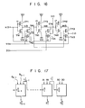
- Fig. 17 shows a parallel adder circuit to which the full adder according to the present invention is applied.
- Aj and Bj 0 to n-1
- a carry input signal from a lower bit is defined as
- a sum output signal is defined as Si
- a carry output signal to an upper bit is defined as .
- the full adders of the present invention are aligned to be parallel to each other.
- the carry output signal from the lower-bit full adder is supplied as the carry input signal to the adjacent higher-bit full adder.
- Each full adder receives two input signals each of which corresponds to each bit and the carry output signal from the immediately preceding lower-bit full adder to obtain a sum output signal and a carry output signal.
- the carry input signal is assigned to the input signal Z, high-speed operation of the full adders can be achieved. Since two input signals are supplied in advance to each full adder, the carry input signal supplied from the immediately preceding lower-bit full adder determines the operation speed of the parallel adder.
Landscapes
- Physics & Mathematics (AREA)
- General Physics & Mathematics (AREA)
- Engineering & Computer Science (AREA)
- Computational Mathematics (AREA)
- Mathematical Analysis (AREA)
- Pure & Applied Mathematics (AREA)
- Theoretical Computer Science (AREA)
- Computing Systems (AREA)
- Mathematical Optimization (AREA)
- General Engineering & Computer Science (AREA)
- Electronic Switches (AREA)
Applications Claiming Priority (2)
| Application Number | Priority Date | Filing Date | Title |
|---|---|---|---|
| JP56194768A JPS5896347A (ja) | 1981-12-03 | 1981-12-03 | 全加算器 |
| JP194768/81 | 1981-12-03 |
Publications (3)
| Publication Number | Publication Date |
|---|---|
| EP0081052A2 true EP0081052A2 (fr) | 1983-06-15 |
| EP0081052A3 EP0081052A3 (en) | 1986-02-05 |
| EP0081052B1 EP0081052B1 (fr) | 1988-12-28 |
Family
ID=16329911
Family Applications (1)
| Application Number | Title | Priority Date | Filing Date |
|---|---|---|---|
| EP82108974A Expired EP0081052B1 (fr) | 1981-12-03 | 1982-09-28 | Additionneur complet et circuit d'opération comportant une pluralité d'additionneurs complets |
Country Status (4)
| Country | Link |
|---|---|
| US (1) | US4592007A (fr) |
| EP (1) | EP0081052B1 (fr) |
| JP (1) | JPS5896347A (fr) |
| DE (1) | DE3279313D1 (fr) |
Families Citing this family (12)
| Publication number | Priority date | Publication date | Assignee | Title |
|---|---|---|---|---|
| JPS60134932A (ja) * | 1983-12-24 | 1985-07-18 | Toshiba Corp | プリチヤ−ジ型の桁上げ連鎖加算回路 |
| US4709346A (en) * | 1985-04-01 | 1987-11-24 | Raytheon Company | CMOS subtractor |
| ATE85852T1 (de) * | 1985-09-30 | 1993-03-15 | Siemens Ag | Addierzelle fuer carry-ripple-addierer in cmostechnik. |
| ATE84155T1 (de) * | 1985-09-30 | 1993-01-15 | Siemens Ag | Mehrstelliger carry-ripple-addierer in cmostechnik mit zwei typen von addiererzellen. |
| JPH07104774B2 (ja) * | 1985-11-26 | 1995-11-13 | 株式会社東芝 | 同期式演算回路 |
| US5138959A (en) * | 1988-09-15 | 1992-08-18 | Prabhakar Kulkarni | Method for treatment of hazardous waste in absence of oxygen |
| FR2716759B1 (fr) * | 1994-02-28 | 1996-04-05 | Sgs Thomson Microelectronics | Etage de formatage d'opérandes optimisé. |
| US5875124A (en) * | 1995-02-22 | 1999-02-23 | Texas Instruments Japan Ltd. | Full adder circuit |
| US5719528A (en) * | 1996-04-23 | 1998-02-17 | Phonak Ag | Hearing aid device |
| US6356112B1 (en) | 2000-03-28 | 2002-03-12 | Translogic Technology, Inc. | Exclusive or/nor circuit |
| US7260595B2 (en) * | 2002-12-23 | 2007-08-21 | Arithmatica Limited | Logic circuit and method for carry and sum generation and method of designing such a logic circuit |
| US7170317B2 (en) * | 2003-05-23 | 2007-01-30 | Arithmatica Limited | Sum bit generation circuit |
Family Cites Families (6)
| Publication number | Priority date | Publication date | Assignee | Title |
|---|---|---|---|---|
| US3602705A (en) * | 1970-03-25 | 1971-08-31 | Westinghouse Electric Corp | Binary full adder circuit |
| US3767906A (en) * | 1972-01-21 | 1973-10-23 | Rca Corp | Multifunction full adder |
| US3843876A (en) * | 1973-09-20 | 1974-10-22 | Motorola Inc | Electronic digital adder having a high speed carry propagation line |
| US4054788A (en) * | 1976-06-04 | 1977-10-18 | Hewlett-Packard Company | Modular binary half-adder |
| US4254471A (en) * | 1978-04-25 | 1981-03-03 | International Computers Limited | Binary adder circuit |
| US4463439A (en) * | 1982-05-17 | 1984-07-31 | International Business Machines Corporation | Sum and carry outputs with shared subfunctions |
-
1981
- 1981-12-03 JP JP56194768A patent/JPS5896347A/ja active Granted
-
1982
- 1982-09-28 DE DE8282108974T patent/DE3279313D1/de not_active Expired
- 1982-09-28 EP EP82108974A patent/EP0081052B1/fr not_active Expired
- 1982-09-29 US US06/428,033 patent/US4592007A/en not_active Expired - Lifetime
Also Published As
| Publication number | Publication date |
|---|---|
| JPS5896347A (ja) | 1983-06-08 |
| EP0081052B1 (fr) | 1988-12-28 |
| JPS6224815B2 (fr) | 1987-05-30 |
| EP0081052A3 (en) | 1986-02-05 |
| DE3279313D1 (en) | 1989-02-02 |
| US4592007A (en) | 1986-05-27 |
Similar Documents
| Publication | Publication Date | Title |
|---|---|---|
| EP0081052A2 (fr) | Additionneur complet et circuit d'opération comportant une pluralité d'additionneurs complets | |
| US4573137A (en) | Adder circuit | |
| Ohkubo et al. | A 4.4 ns CMOS 54/spl times/54-b multiplier using pass-transistor multiplexer | |
| US4761760A (en) | Digital adder-subtracter with tentative result correction circuit | |
| EP0328063A2 (fr) | Circuit de calcul de valeur absolue ayant un seul additionneur | |
| EP0096333A2 (fr) | Additionneur complet | |
| US20220012015A1 (en) | Integrated circuits with machine learning extensions | |
| GB2145857A (en) | Up/down counter | |
| US5303175A (en) | Floating point arithmetic unit | |
| US4764888A (en) | N-bit carry select adder circuit with double carry select generation | |
| EP0143456A2 (fr) | Circuit d'addition parallèle | |
| US4775810A (en) | Parity check logic circuit | |
| US4122527A (en) | Emitter coupled multiplier array | |
| US5177703A (en) | Division circuit using higher radices | |
| US20030120694A1 (en) | Method and apparatus for use in booth-encoded multiplication | |
| US4349888A (en) | CMOS Static ALU | |
| US4086657A (en) | Five-stage four-bit complex multiplier | |
| US6489811B2 (en) | Logic gate with symmetrical propagation delay from any input to any output and a controlled output pulse width | |
| EP0249040B1 (fr) | Circuit de conversion selon Booth | |
| US5457723A (en) | Barrel shifter having CMOS structure integrated on MOS integrated circuits | |
| JPH0254670B2 (fr) | ||
| US7487198B2 (en) | Multibit bit adder | |
| US4160290A (en) | One-bit multifunction arithmetic and logic circuit | |
| EP0242600A2 (fr) | Procédé de calculation de retenue anticipée et circuits à cet effet | |
| EP0267425A2 (fr) | Multiplieurs numériques binaires à structure matricielle |
Legal Events
| Date | Code | Title | Description |
|---|---|---|---|
| PUAI | Public reference made under article 153(3) epc to a published international application that has entered the european phase |
Free format text: ORIGINAL CODE: 0009012 |
|
| 17P | Request for examination filed |
Effective date: 19820928 |
|
| AK | Designated contracting states |
Designated state(s): DE FR GB IT |
|
| RAP1 | Party data changed (applicant data changed or rights of an application transferred) |
Owner name: KABUSHIKI KAISHA TOSHIBA |
|
| PUAL | Search report despatched |
Free format text: ORIGINAL CODE: 0009013 |
|
| AK | Designated contracting states |
Designated state(s): DE FR GB IT |
|
| 17Q | First examination report despatched |
Effective date: 19870818 |
|
| GRAA | (expected) grant |
Free format text: ORIGINAL CODE: 0009210 |
|
| AK | Designated contracting states |
Kind code of ref document: B1 Designated state(s): DE FR GB IT |
|
| ITF | It: translation for a ep patent filed | ||
| REF | Corresponds to: |
Ref document number: 3279313 Country of ref document: DE Date of ref document: 19890202 |
|
| ET | Fr: translation filed | ||
| PLBE | No opposition filed within time limit |
Free format text: ORIGINAL CODE: 0009261 |
|
| STAA | Information on the status of an ep patent application or granted ep patent |
Free format text: STATUS: NO OPPOSITION FILED WITHIN TIME LIMIT |
|
| 26N | No opposition filed | ||
| ITTA | It: last paid annual fee | ||
| PGFP | Annual fee paid to national office [announced via postgrant information from national office to epo] |
Ref country code: FR Payment date: 19970909 Year of fee payment: 16 |
|
| PGFP | Annual fee paid to national office [announced via postgrant information from national office to epo] |
Ref country code: GB Payment date: 19970919 Year of fee payment: 16 |
|
| PGFP | Annual fee paid to national office [announced via postgrant information from national office to epo] |
Ref country code: DE Payment date: 19971010 Year of fee payment: 16 |
|
| PG25 | Lapsed in a contracting state [announced via postgrant information from national office to epo] |
Ref country code: GB Free format text: LAPSE BECAUSE OF NON-PAYMENT OF DUE FEES Effective date: 19980928 |
|
| GBPC | Gb: european patent ceased through non-payment of renewal fee |
Effective date: 19980928 |
|
| PG25 | Lapsed in a contracting state [announced via postgrant information from national office to epo] |
Ref country code: FR Free format text: LAPSE BECAUSE OF NON-PAYMENT OF DUE FEES Effective date: 19990531 |
|
| PG25 | Lapsed in a contracting state [announced via postgrant information from national office to epo] |
Ref country code: DE Free format text: LAPSE BECAUSE OF NON-PAYMENT OF DUE FEES Effective date: 19990701 |
|
| REG | Reference to a national code |
Ref country code: FR Ref legal event code: ST |