EP0081819A2 - Auswahlschalter für ein konkurrierendes Prozessorennetzwerk - Google Patents
Auswahlschalter für ein konkurrierendes Prozessorennetzwerk Download PDFInfo
- Publication number
- EP0081819A2 EP0081819A2 EP82111434A EP82111434A EP0081819A2 EP 0081819 A2 EP0081819 A2 EP 0081819A2 EP 82111434 A EP82111434 A EP 82111434A EP 82111434 A EP82111434 A EP 82111434A EP 0081819 A2 EP0081819 A2 EP 0081819A2
- Authority
- EP
- European Patent Office
- Prior art keywords
- clear
- signal
- circuit means
- output
- selection
- Prior art date
- Legal status (The legal status is an assumption and is not a legal conclusion. Google has not performed a legal analysis and makes no representation as to the accuracy of the status listed.)
- Granted
Links
Images



Classifications
-
- G—PHYSICS
- G06—COMPUTING OR CALCULATING; COUNTING
- G06F—ELECTRIC DIGITAL DATA PROCESSING
- G06F13/00—Interconnection of, or transfer of information or other signals between, memories, input/output devices or central processing units
- G06F13/14—Handling requests for interconnection or transfer
-
- G—PHYSICS
- G06—COMPUTING OR CALCULATING; COUNTING
- G06F—ELECTRIC DIGITAL DATA PROCESSING
- G06F13/00—Interconnection of, or transfer of information or other signals between, memories, input/output devices or central processing units
- G06F13/38—Information transfer, e.g. on bus
- G06F13/40—Bus structure
- G06F13/4004—Coupling between buses
- G06F13/4022—Coupling between buses using switching circuits, e.g. switching matrix, connection or expansion network
-
- G—PHYSICS
- G06—COMPUTING OR CALCULATING; COUNTING
- G06F—ELECTRIC DIGITAL DATA PROCESSING
- G06F15/00—Digital computers in general; Data processing equipment in general
- G06F15/76—Architectures of general purpose stored program computers
- G06F15/80—Architectures of general purpose stored program computers comprising an array of processing units with common control, e.g. single instruction multiple data processors
Definitions
- This invention relates to a selector switch for an asynchronous network of concurrent processors and more particularly to such a switch which is adapted to be cleared when it is part of the node in the network that has become clogged by a message passing through the network.
- Arbiter switches and selector switches are employed in the formation of networks for asynchronous transmission from one source node to one of a number of destinations in the network.
- An arbiter switch is a switch or node which receives such asynchronous transmission from one of two different input ports and transfers that message in an asynchronous manner to its output port.
- Such an arbiter switch is disclosed in detail in the Clark U.S. Patent No. 4,251,879 which is assigned to the assignee of the present invention.
- a selector switch is a switch which receives a message on its input port and transmits it to one of two output ports according to the first bit in the serial transmission to be received. Such a selector switch is disclosed in the Clark U.S. Patent No.
- one node when it is desired for one node to transmit a message to another node, it begins its transmission which establishes a path between respective nodes, which path becomes dedicated to that transmission until an end-of-message signal is received by the destination and an acknowledge end-of-message signal is transmitted back through the various switches of the network forming the path to the source.
- This causes a delay in freeing the network for the establishment of different transmission paths due to the time that it takes for the end-of-message signal to reach the destination and the acknowledge end-of-message signal to be transmitted back to the source.
- an object of the present invention to provide an improved selector switch for an asynchronous network of concurrent processors.
- the present invention is directed toward a selector switch to receive a transmission on its input port and to transmit that message to one of two different output ports.
- the selector switch also is adapted to receive a clear signal on its input port which resets the switch to its idle state and transmits that clear signal on to the selected output port when the switch is not in its idle state.
- a feature then of the present invention resides in a selector switch which is adapted to be set to its idle state by a clear signal received on its input port and to transmit that clear signal on to a previously selected output port.
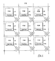
- FIG. 1 A concurrent network of processors, or more particularly processor and storage modules, is illustrated in Figure 1 wherein the respective processor storage modules 10 are coupled together by a nearest neighbor switching network that is formed of hexagonal configurations 11 of speed independent arbiter and selector switches.
- a nearest neighbor switching network that is formed of hexagonal configurations 11 of speed independent arbiter and selector switches.
- three hexagonal configurations 11 are required for coupling the corresponding processor storage module 10 to the network.
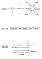
- FIG 2 A more detailed illustration of a respective hexagonal configuration is illustrated in Figure 2 where three arbiter switches 12 and three selector switches 13 are employed.
- Such a hexagonal configuration receives transmission from three different sources and provides transmission to three different destinations and it is for this reason that the configurations are illustrated in Figure 1 by triangular symbols 11 and that three such configurations are required to couple each processor storage module to its four nearest neighbors in a rectangular matrix-type of network.
- each of the processor storage modules of Figure 1 is provided with a corresponding communication's interface 10a which includes a parallel-to-serial buffer register since the data transfer between the processor and the memory of the respective modules would normally be in a parallel manner.
- FIG 3A The format of such message transmission is illustrated in Figure 3A and begins with (from right to left) the routing field which is then followed by a destination name, source name, data being transmitted, an error-checking field, and an end-of-message signal.
- the interface between the respective switches is illustrated in Figure 3B, it being understood that two such interfaces are required for transmissions in opposite directions.
- Each interface includes a data group of signal lines and a clear group of signal lines.
- the data group is made up of three signal lines in the forward direction, "T" (true), “F” (false), and “E” (end) to signal the end-of-message.
- the data group also includes a "VEFT” (vacant end, false, true) to acknowledge the transmission of each of the data characters, which acknowledgment is required between the respective switches to accommodate asynchronous transmission.
- the clear group of signal lines employs a forward signal “C” (clear) and a reverse signal “VC” (vacant clear).
- C forward signal
- VC reverse signal
- the clear group of signals is employed for clearing or resetting one or more transmission paths in the event that the transmission path becomes locked in or "stuck” due to any malfunction which prevents the completion of the message transmission. It will be appreciated that without the "clear” feature, any purely asynchronous system can become “stuck” as the system cannot distinguish between an event that has not yet occurred (but eventually will) and one that will never occur. Thus, whenever a transmitting processor determines that a desired transmission path has become “stuck”, that processor will issue a clear signal to clear a path through the network. Any messages that may be corrupted by the clear will eventually be'retransmitted by their sender.
- the arbiter of the present invention makes wide use of consensus gates or C-elements which in essence are memory devices with two or more inputs and one output such that the C-element retains its previous state as long as its inputs do not agree with each other, . but tends toward the state of the inputs whenever they contain identical values. That is to say, such a C-element is a latch type device which retains its previous state until such time as all of its inputs have changed to the same state.
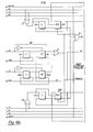
- the arbiter switch of the present invention is illustrated in Figures 4A and 4B and will now be described. It is to be remembered that the arbiter switch receives signals from two different inputs and routes them to a single output. In the present invention, the arbiter switch reacts to a change in signal levels as distinct from the actual voltage levels themselves. That is to say, the input ports have edge detection capability.
- input consensus gates 20 and 20a are consensus gates that respond to signal changes on input lines F0, T0, and Tl, Fl respectively by way of OR gates 21 and 21a.
- the specific circuitry of consensus gates 20 and 20a is illustrated in Figure 6A.
- the inverted outputs of the respective input circuits 20 and 20a are supplied along with the corresponding input signals to consensus gates 22 and 22a respectively where the edge detection is performed.
- the actual circuitry of consensus gates 22 and 22a is illustrated in Figure 6E.
- Arbitration circuitry 23 receives the output signals of the respective edge detectors 22 and 22a and generates one of two output signals indicating which of edge detectors 22 and 22a was the first to detect a signal change on its corresponding input line. The output of arbitration circuitry 23 then chooses the appropriate input port for the transfer of that signal through the arbiter to the output port.
- the respective C-gates 24 and 24a are to receive and store either a true or false signal T 0 or F 0 (or T 1 or F l ) respectively.
- the actual circuitry of these C-gates is illustrated in Figure 6D.
- the C-gates 25 and 25a are for receiving the corresponding end-of-message signals E 0 or E l respectively.
- the actual circuitry for these C-gates is illustrated in Figure 6E.
- the corresponding signal selected for transmission to the next node is then supplied thereto by way of OR gates 26.
- the clear circuitry 28 of the arbiter receives a clear signal CO or Cl from one of two input ports which sets the clear input C-gates 29 or 29a respectively and transfers that signal to the clear enable C-gates 30 and 30a.
- the output signals from either one of these C-gates then resets the circuitry by way of OR gate 31 and the clear receipt acknowledgment is sent back by the inverted output of one of the respective consensus gates 29 or 29a.
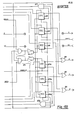
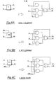
- the selector switch of the present invention is illustrated in detail in Figures 5A and 5B. It will be remembered that the selector switch receives a message on its single input port and routes that message to one of two output ports according to the first bit in the serial transmission of the message, which bit is discarded at the time of selection.
- the first incoming bit of the message is received by either consensus gate 40 or 40a depending upon whether it is a true or false signal.
- the corresponding gate generates an acknowledge signal which is transmitted back to the sender by way of AND gate 46 and also sets the corresponding consensus enable gate 41 or 41a which selects the appropriate.output port for transmission of the remaining portion of the routing field and the message.
- This first bit has now been discarded.
- Detailed schematics of C-gates 40 and 40a are illustrated in Figure 6A and detailed schematic diagrams of C-gates 41 and 4la are illustrated in Figure 6D.
- the two output ports are shown in Figure 5B and are respectively either C-gates 42a, 42b and 42c, or 43a, 43b and 43c.
- Schematic diagrams of gates 42a and 43a are illustrated in Figure 6E while the schematic diagrams of C-gates 42b and 42c and 43b and 43c are illustrated in Figure 6D.
- the selector switch When the CLEAR signal of the present invention is received by the selector switch, it serves to clear all the gates of Figure 5A and also to set C-gates 44a or 44b for the selected output port. This serves to transmit that clear signal on to that one of the output ports which has been selected so as to pass the clear signal on to the next switch in the transmission path.
- An arbiter switch and a selector switch have been described from which an asynchronous network of concurrent processors can be formed where the arbiter switch receives a message from one of two input ports and transmits it to its output port while the selector switch receives a message from one input port and transmits it to one of two output ports in accordance with the first bit in the serial message.
- a path through the network which has been established can be cleared should it become apparent that that particular path has become locked in due to a malfunction of a component in one of the nodes or switches in the network.
Landscapes
- Engineering & Computer Science (AREA)
- Theoretical Computer Science (AREA)
- Physics & Mathematics (AREA)
- General Engineering & Computer Science (AREA)
- Computer Hardware Design (AREA)
- General Physics & Mathematics (AREA)
- Mathematical Physics (AREA)
- Computing Systems (AREA)
- Multi Processors (AREA)
- Data Exchanges In Wide-Area Networks (AREA)
Applications Claiming Priority (2)
| Application Number | Priority Date | Filing Date | Title |
|---|---|---|---|
| US06/329,423 US4498133A (en) | 1981-12-10 | 1981-12-10 | Selector switch for a concurrent network of processors |
| US329423 | 1981-12-10 |
Publications (3)
| Publication Number | Publication Date |
|---|---|
| EP0081819A2 true EP0081819A2 (de) | 1983-06-22 |
| EP0081819A3 EP0081819A3 (en) | 1986-01-15 |
| EP0081819B1 EP0081819B1 (de) | 1989-08-09 |
Family
ID=23285318
Family Applications (1)
| Application Number | Title | Priority Date | Filing Date |
|---|---|---|---|
| EP82111434A Expired EP0081819B1 (de) | 1981-12-10 | 1982-12-09 | Auswahlschalter für ein konkurrierendes Prozessorennetzwerk |
Country Status (5)
| Country | Link |
|---|---|
| US (1) | US4498133A (de) |
| EP (1) | EP0081819B1 (de) |
| JP (1) | JPS58502071A (de) |
| DE (1) | DE3279869D1 (de) |
| WO (1) | WO1983002181A1 (de) |
Cited By (1)
| Publication number | Priority date | Publication date | Assignee | Title |
|---|---|---|---|---|
| EP0146275A3 (de) * | 1983-12-16 | 1987-04-15 | Gec Plessey Telecommunications Limited | Datenvermittlungssystem |
Families Citing this family (32)
| Publication number | Priority date | Publication date | Assignee | Title |
|---|---|---|---|---|
| US5146606A (en) * | 1986-09-18 | 1992-09-08 | Digital Equipment Corporation | Systems for interconnecting and configuring plurality of memory elements by control of mode signals |
| US5230079A (en) * | 1986-09-18 | 1993-07-20 | Digital Equipment Corporation | Massively parallel array processing system with processors selectively accessing memory module locations using address in microword or in address register |
| US6108763A (en) * | 1986-09-18 | 2000-08-22 | Grondalski; Robert S. | Simultaneous parity generating/reading circuit for massively parallel processing systems |
| US4985832A (en) * | 1986-09-18 | 1991-01-15 | Digital Equipment Corporation | SIMD array processing system with routing networks having plurality of switching stages to transfer messages among processors |
| US5010477A (en) * | 1986-10-17 | 1991-04-23 | Hitachi, Ltd. | Method and apparatus for transferring vector data between parallel processing system with registers & logic for inter-processor data communication independents of processing operations |
| US5113502A (en) * | 1986-11-20 | 1992-05-12 | Allen-Bradley Company, Inc. | Method and apparatus for saving and performing industrial control commands |
| US4891751A (en) * | 1987-03-27 | 1990-01-02 | Floating Point Systems, Inc. | Massively parallel vector processing computer |
| US5070446A (en) * | 1988-11-13 | 1991-12-03 | Thinking Machines Corporation | Method of simulating a hexagonal array of computer processors and/or memories |
| US4974190A (en) * | 1988-12-05 | 1990-11-27 | Digital Equipment Corporation | Pass-through and isolation switch |
| US5963745A (en) * | 1990-11-13 | 1999-10-05 | International Business Machines Corporation | APAP I/O programmable router |
| US5966528A (en) * | 1990-11-13 | 1999-10-12 | International Business Machines Corporation | SIMD/MIMD array processor with vector processing |
| US5625836A (en) * | 1990-11-13 | 1997-04-29 | International Business Machines Corporation | SIMD/MIMD processing memory element (PME) |
| US5752067A (en) * | 1990-11-13 | 1998-05-12 | International Business Machines Corporation | Fully scalable parallel processing system having asynchronous SIMD processing |
| US5590345A (en) * | 1990-11-13 | 1996-12-31 | International Business Machines Corporation | Advanced parallel array processor(APAP) |
| EP0485690B1 (de) * | 1990-11-13 | 1999-05-26 | International Business Machines Corporation | Paralleles Assoziativprozessor-System |
| US5617577A (en) * | 1990-11-13 | 1997-04-01 | International Business Machines Corporation | Advanced parallel array processor I/O connection |
| US5765015A (en) * | 1990-11-13 | 1998-06-09 | International Business Machines Corporation | Slide network for an array processor |
| US5588152A (en) * | 1990-11-13 | 1996-12-24 | International Business Machines Corporation | Advanced parallel processor including advanced support hardware |
| US5794059A (en) * | 1990-11-13 | 1998-08-11 | International Business Machines Corporation | N-dimensional modified hypercube |
| US5815723A (en) * | 1990-11-13 | 1998-09-29 | International Business Machines Corporation | Picket autonomy on a SIMD machine |
| US5734921A (en) * | 1990-11-13 | 1998-03-31 | International Business Machines Corporation | Advanced parallel array processor computer package |
| US5828894A (en) * | 1990-11-13 | 1998-10-27 | International Business Machines Corporation | Array processor having grouping of SIMD pickets |
| US5809292A (en) * | 1990-11-13 | 1998-09-15 | International Business Machines Corporation | Floating point for simid array machine |
| US5963746A (en) * | 1990-11-13 | 1999-10-05 | International Business Machines Corporation | Fully distributed processing memory element |
| US5630162A (en) * | 1990-11-13 | 1997-05-13 | International Business Machines Corporation | Array processor dotted communication network based on H-DOTs |
| US5765012A (en) * | 1990-11-13 | 1998-06-09 | International Business Machines Corporation | Controller for a SIMD/MIMD array having an instruction sequencer utilizing a canned routine library |
| US5765011A (en) * | 1990-11-13 | 1998-06-09 | International Business Machines Corporation | Parallel processing system having a synchronous SIMD processing with processing elements emulating SIMD operation using individual instruction streams |
| US5594918A (en) * | 1991-05-13 | 1997-01-14 | International Business Machines Corporation | Parallel computer system providing multi-ported intelligent memory |
| JP2642039B2 (ja) * | 1992-05-22 | 1997-08-20 | インターナショナル・ビジネス・マシーンズ・コーポレイション | アレイ・プロセッサ |
| US5598568A (en) * | 1993-05-06 | 1997-01-28 | Mercury Computer Systems, Inc. | Multicomputer memory access architecture |
| JP3483284B2 (ja) * | 1993-12-28 | 2004-01-06 | 富士通株式会社 | 並列プロセッサシステム用ネットワークサブ装置および並列プロセッサシステム用ネットワーク装置 |
| JP2886093B2 (ja) * | 1994-07-28 | 1999-04-26 | 株式会社日立製作所 | 障害処理方法および情報処理システム |
Family Cites Families (12)
| Publication number | Priority date | Publication date | Assignee | Title |
|---|---|---|---|---|
| US3810105A (en) * | 1967-10-26 | 1974-05-07 | Xerox Corp | Computer input-output system |
| US3962706A (en) * | 1974-03-29 | 1976-06-08 | Massachusetts Institute Of Technology | Data processing apparatus for highly parallel execution of stored programs |
| US4161718A (en) * | 1977-06-20 | 1979-07-17 | Motorola Israel Ltd. | Supervisory control system |
| JPS547252A (en) * | 1977-06-20 | 1979-01-19 | Hitachi Ltd | Program control system |
| US4231087A (en) * | 1978-10-18 | 1980-10-28 | Bell Telephone Laboratories, Incorporated | Microprocessor support system |
| US4307446A (en) * | 1979-05-02 | 1981-12-22 | Burroughs Corporation | Digital communication networks employing speed independent switches |
| US4237447A (en) * | 1979-05-02 | 1980-12-02 | Burroughs Corporation | Speed independent selector switch for digital communication networks |
| US4365313A (en) * | 1980-04-11 | 1982-12-21 | Sony Corporation | Cue control apparatus |
| US4320386A (en) * | 1980-07-30 | 1982-03-16 | General Electric Company | Selection and power reset circuit |
| US4412285A (en) * | 1981-04-01 | 1983-10-25 | Teradata Corporation | Multiprocessor intercommunication system and method |
| JPS588359A (ja) * | 1981-07-07 | 1983-01-18 | バロース コーポレーション | 還元プロセサの同時処理回路網および処理方法 |
| US4451898A (en) * | 1981-11-09 | 1984-05-29 | Hewlett-Packard Company | Asynchronous interface message transmission using source and receive devices |
-
1981
- 1981-12-10 US US06/329,423 patent/US4498133A/en not_active Expired - Lifetime
-
1982
- 1982-12-06 JP JP83500317A patent/JPS58502071A/ja active Granted
- 1982-12-06 WO PCT/US1982/001706 patent/WO1983002181A1/en not_active Ceased
- 1982-12-09 EP EP82111434A patent/EP0081819B1/de not_active Expired
- 1982-12-09 DE DE8282111434T patent/DE3279869D1/de not_active Expired
Cited By (1)
| Publication number | Priority date | Publication date | Assignee | Title |
|---|---|---|---|---|
| EP0146275A3 (de) * | 1983-12-16 | 1987-04-15 | Gec Plessey Telecommunications Limited | Datenvermittlungssystem |
Also Published As
| Publication number | Publication date |
|---|---|
| EP0081819A3 (en) | 1986-01-15 |
| WO1983002181A1 (en) | 1983-06-23 |
| JPS6338734B2 (de) | 1988-08-02 |
| JPS58502071A (ja) | 1983-12-01 |
| US4498133A (en) | 1985-02-05 |
| EP0081819B1 (de) | 1989-08-09 |
| DE3279869D1 (en) | 1989-09-14 |
Similar Documents
| Publication | Publication Date | Title |
|---|---|---|
| US4498133A (en) | Selector switch for a concurrent network of processors | |
| US4482996A (en) | Five port module as a node in an asynchronous speed independent network of concurrent processors | |
| US4488151A (en) | Arbiter switch for a concurrent network of processors | |
| EP0018755B1 (de) | Digitale Nachrichtennetze mit von der Geschwindigkeit unabhängigen Schaltern | |
| US6314487B1 (en) | Adaptive routing controller of a crossbar core module used in a crossbar routing switch | |
| US4965788A (en) | Self-routing switch element for an asynchronous time switch | |
| EP0022170B1 (de) | Verfahren zur Übertragung von Datenpaketen in einem örtlich gemeinsam benutzten Busleitungsnetzwerk und örtlich gemeinsam benutztes Busleitungsnetzwerk | |
| US4380063A (en) | Flow control mechanism for block switching nodes | |
| US5654695A (en) | Multi-function network | |
| US5367518A (en) | Self-routing switching element and fast packet switch | |
| EP0104801B1 (de) | Vierwegarbiterschalter für ein Fünfportmodul als Knoten in einem asynchronen geschwindigkeitsunabhängigen Netzwerk von konkurrierenden Prozessoren | |
| EP0229299A2 (de) | Ein blockierungsfreies selbstsuchendes Paket- und Leitungsvermittlungsnetzwerk | |
| US4984237A (en) | Multistage network with distributed pipelined control | |
| EP0018756B1 (de) | Geschwindigkeitsunabhängiger Entscheidungsschalter für digitale Übertragungsnetzwerke | |
| JPS6184943A (ja) | 自己ルーテイングパケツトおよび回線交換方式 | |
| US4314233A (en) | Four-wire speed independent arbiter switch for digital communication networks | |
| JPS6340383B2 (de) | ||
| US4276611A (en) | Device for the control of data flows | |
| US4484325A (en) | Four way selector switch for a five port module as a node asynchronous speed independent network of concurrent processors | |
| US4307378A (en) | Four-wire speed independent selector switch for digital communication networks | |
| JPS63257052A (ja) | マルチプロセツサシステム | |
| JPH0414164A (ja) | コンピュータネットワークシステム | |
| JPH05242000A (ja) | 多段ネットワークシステム | |
| JPH0253983B2 (de) | ||
| KR920013159A (ko) | 인터커넥션 네트워크 스위칭소자 |
Legal Events
| Date | Code | Title | Description |
|---|---|---|---|
| PUAI | Public reference made under article 153(3) epc to a published international application that has entered the european phase |
Free format text: ORIGINAL CODE: 0009012 |
|
| AK | Designated contracting states |
Designated state(s): BE DE FR GB IT NL SE |
|
| PUAL | Search report despatched |
Free format text: ORIGINAL CODE: 0009013 |
|
| AK | Designated contracting states |
Designated state(s): BE DE FR GB IT NL SE |
|
| 17P | Request for examination filed |
Effective date: 19860129 |
|
| RAP1 | Party data changed (applicant data changed or rights of an application transferred) |
Owner name: BURROUGHS CORPORATION (A DELAWARE CORPORATION) |
|
| 17Q | First examination report despatched |
Effective date: 19870506 |
|
| GRAA | (expected) grant |
Free format text: ORIGINAL CODE: 0009210 |
|
| AK | Designated contracting states |
Kind code of ref document: B1 Designated state(s): BE DE FR GB IT NL SE |
|
| REF | Corresponds to: |
Ref document number: 3279869 Country of ref document: DE Date of ref document: 19890914 |
|
| ET | Fr: translation filed | ||
| ITF | It: translation for a ep patent filed | ||
| PLBE | No opposition filed within time limit |
Free format text: ORIGINAL CODE: 0009261 |
|
| STAA | Information on the status of an ep patent application or granted ep patent |
Free format text: STATUS: NO OPPOSITION FILED WITHIN TIME LIMIT |
|
| 26N | No opposition filed | ||
| PGFP | Annual fee paid to national office [announced via postgrant information from national office to epo] |
Ref country code: SE Payment date: 19921118 Year of fee payment: 11 |
|
| ITTA | It: last paid annual fee | ||
| PGFP | Annual fee paid to national office [announced via postgrant information from national office to epo] |
Ref country code: NL Payment date: 19921231 Year of fee payment: 11 |
|
| PGFP | Annual fee paid to national office [announced via postgrant information from national office to epo] |
Ref country code: BE Payment date: 19930114 Year of fee payment: 11 |
|
| PG25 | Lapsed in a contracting state [announced via postgrant information from national office to epo] |
Ref country code: SE Effective date: 19931210 |
|
| PG25 | Lapsed in a contracting state [announced via postgrant information from national office to epo] |
Ref country code: BE Effective date: 19931231 |
|
| BERE | Be: lapsed |
Owner name: BURROUGHS CORP. (A DELAWARE CORP.) Effective date: 19931231 |
|
| PG25 | Lapsed in a contracting state [announced via postgrant information from national office to epo] |
Ref country code: NL Effective date: 19940701 |
|
| NLV4 | Nl: lapsed or anulled due to non-payment of the annual fee | ||
| PGFP | Annual fee paid to national office [announced via postgrant information from national office to epo] |
Ref country code: FR Payment date: 19941209 Year of fee payment: 13 |
|
| PGFP | Annual fee paid to national office [announced via postgrant information from national office to epo] |
Ref country code: DE Payment date: 19941223 Year of fee payment: 13 |
|
| EUG | Se: european patent has lapsed |
Ref document number: 82111434.5 Effective date: 19940710 |
|
| PG25 | Lapsed in a contracting state [announced via postgrant information from national office to epo] |
Ref country code: FR Effective date: 19960830 |
|
| PG25 | Lapsed in a contracting state [announced via postgrant information from national office to epo] |
Ref country code: DE Effective date: 19960903 |
|
| REG | Reference to a national code |
Ref country code: FR Ref legal event code: ST |
|
| PGFP | Annual fee paid to national office [announced via postgrant information from national office to epo] |
Ref country code: GB Payment date: 19961108 Year of fee payment: 15 |
|
| PG25 | Lapsed in a contracting state [announced via postgrant information from national office to epo] |
Ref country code: GB Free format text: LAPSE BECAUSE OF NON-PAYMENT OF DUE FEES Effective date: 19971209 |
|
| GBPC | Gb: european patent ceased through non-payment of renewal fee |
Effective date: 19971209 |