EP0081863A2 - Appareil de commande pour faire fonctionner une lampe à décharge - Google Patents
Appareil de commande pour faire fonctionner une lampe à décharge Download PDFInfo
- Publication number
- EP0081863A2 EP0081863A2 EP82200903A EP82200903A EP0081863A2 EP 0081863 A2 EP0081863 A2 EP 0081863A2 EP 82200903 A EP82200903 A EP 82200903A EP 82200903 A EP82200903 A EP 82200903A EP 0081863 A2 EP0081863 A2 EP 0081863A2
- Authority
- EP
- European Patent Office
- Prior art keywords
- lamp
- circuit
- current
- voltage
- resistor
- Prior art date
- Legal status (The legal status is an assumption and is not a legal conclusion. Google has not performed a legal analysis and makes no representation as to the accuracy of the status listed.)
- Withdrawn
Links
- 238000004804 winding Methods 0.000 claims abstract description 92
- 230000001965 increasing effect Effects 0.000 claims abstract description 9
- 230000001939 inductive effect Effects 0.000 claims description 6
- 230000001419 dependent effect Effects 0.000 claims description 2
- 230000001681 protective effect Effects 0.000 claims description 2
- 239000007787 solid Substances 0.000 abstract 4
- 206010065929 Cardiovascular insufficiency Diseases 0.000 abstract 1
- 230000002411 adverse Effects 0.000 abstract 1
- 239000004020 conductor Substances 0.000 description 13
- 239000003990 capacitor Substances 0.000 description 11
- 239000011734 sodium Substances 0.000 description 9
- 229910052708 sodium Inorganic materials 0.000 description 9
- DGAQECJNVWCQMB-PUAWFVPOSA-M Ilexoside XXIX Chemical compound C[C@@H]1CC[C@@]2(CC[C@@]3(C(=CC[C@H]4[C@]3(CC[C@@H]5[C@@]4(CC[C@@H](C5(C)C)OS(=O)(=O)[O-])C)C)[C@@H]2[C@]1(C)O)C)C(=O)O[C@H]6[C@@H]([C@H]([C@@H]([C@H](O6)CO)O)O)O.[Na+] DGAQECJNVWCQMB-PUAWFVPOSA-M 0.000 description 8
- QSHDDOUJBYECFT-UHFFFAOYSA-N mercury Chemical compound [Hg] QSHDDOUJBYECFT-UHFFFAOYSA-N 0.000 description 8
- 230000008859 change Effects 0.000 description 6
- 230000033228 biological regulation Effects 0.000 description 5
- 230000007423 decrease Effects 0.000 description 5
- 238000010586 diagram Methods 0.000 description 5
- XUIMIQQOPSSXEZ-UHFFFAOYSA-N Silicon Chemical compound [Si] XUIMIQQOPSSXEZ-UHFFFAOYSA-N 0.000 description 4
- 230000015556 catabolic process Effects 0.000 description 4
- 238000000034 method Methods 0.000 description 4
- 229910052710 silicon Inorganic materials 0.000 description 4
- 239000010703 silicon Substances 0.000 description 4
- 230000008901 benefit Effects 0.000 description 3
- 229910001507 metal halide Inorganic materials 0.000 description 3
- 150000005309 metal halides Chemical class 0.000 description 3
- 230000008569 process Effects 0.000 description 3
- 230000001052 transient effect Effects 0.000 description 3
- 230000001960 triggered effect Effects 0.000 description 3
- 230000000694 effects Effects 0.000 description 2
- 238000002955 isolation Methods 0.000 description 2
- 229910044991 metal oxide Inorganic materials 0.000 description 2
- 150000004706 metal oxides Chemical class 0.000 description 2
- 230000004044 response Effects 0.000 description 2
- 230000002441 reversible effect Effects 0.000 description 2
- XEEYBQQBJWHFJM-UHFFFAOYSA-N Iron Chemical group [Fe] XEEYBQQBJWHFJM-UHFFFAOYSA-N 0.000 description 1
- 230000001154 acute effect Effects 0.000 description 1
- 230000000052 comparative effect Effects 0.000 description 1
- 230000003247 decreasing effect Effects 0.000 description 1
- 230000002950 deficient Effects 0.000 description 1
- 230000003111 delayed effect Effects 0.000 description 1
- 230000002939 deleterious effect Effects 0.000 description 1
- 230000001066 destructive effect Effects 0.000 description 1
- 230000006866 deterioration Effects 0.000 description 1
- 230000003628 erosive effect Effects 0.000 description 1
- 238000010438 heat treatment Methods 0.000 description 1
- 230000002452 interceptive effect Effects 0.000 description 1
- 230000004048 modification Effects 0.000 description 1
- 238000012986 modification Methods 0.000 description 1
- 230000000737 periodic effect Effects 0.000 description 1
- 230000002829 reductive effect Effects 0.000 description 1
- 230000003252 repetitive effect Effects 0.000 description 1
Images


Classifications
-
- H—ELECTRICITY
- H05—ELECTRIC TECHNIQUES NOT OTHERWISE PROVIDED FOR
- H05B—ELECTRIC HEATING; ELECTRIC LIGHT SOURCES NOT OTHERWISE PROVIDED FOR; CIRCUIT ARRANGEMENTS FOR ELECTRIC LIGHT SOURCES, IN GENERAL
- H05B41/00—Circuit arrangements or apparatus for igniting or operating discharge lamps
- H05B41/14—Circuit arrangements
- H05B41/26—Circuit arrangements in which the lamp is fed by power derived from DC by means of a converter, e.g. by high-voltage DC
- H05B41/28—Circuit arrangements in which the lamp is fed by power derived from DC by means of a converter, e.g. by high-voltage DC using static converters
-
- H—ELECTRICITY
- H05—ELECTRIC TECHNIQUES NOT OTHERWISE PROVIDED FOR
- H05B—ELECTRIC HEATING; ELECTRIC LIGHT SOURCES NOT OTHERWISE PROVIDED FOR; CIRCUIT ARRANGEMENTS FOR ELECTRIC LIGHT SOURCES, IN GENERAL
- H05B41/00—Circuit arrangements or apparatus for igniting or operating discharge lamps
- H05B41/02—Details
- H05B41/04—Starting switches
- H05B41/042—Starting switches using semiconductor devices
- H05B41/044—Starting switches using semiconductor devices for lamp provided with pre-heating electrodes
- H05B41/046—Starting switches using semiconductor devices for lamp provided with pre-heating electrodes using controlled semiconductor devices
-
- H—ELECTRICITY
- H05—ELECTRIC TECHNIQUES NOT OTHERWISE PROVIDED FOR
- H05B—ELECTRIC HEATING; ELECTRIC LIGHT SOURCES NOT OTHERWISE PROVIDED FOR; CIRCUIT ARRANGEMENTS FOR ELECTRIC LIGHT SOURCES, IN GENERAL
- H05B41/00—Circuit arrangements or apparatus for igniting or operating discharge lamps
- H05B41/14—Circuit arrangements
- H05B41/26—Circuit arrangements in which the lamp is fed by power derived from DC by means of a converter, e.g. by high-voltage DC
- H05B41/28—Circuit arrangements in which the lamp is fed by power derived from DC by means of a converter, e.g. by high-voltage DC using static converters
- H05B41/288—Circuit arrangements in which the lamp is fed by power derived from DC by means of a converter, e.g. by high-voltage DC using static converters with semiconductor devices and specially adapted for lamps without preheating electrodes, e.g. for high-intensity discharge lamps, high-pressure mercury or sodium lamps or low-pressure sodium lamps
- H05B41/2885—Static converters especially adapted therefor; Control thereof
-
- H—ELECTRICITY
- H05—ELECTRIC TECHNIQUES NOT OTHERWISE PROVIDED FOR
- H05B—ELECTRIC HEATING; ELECTRIC LIGHT SOURCES NOT OTHERWISE PROVIDED FOR; CIRCUIT ARRANGEMENTS FOR ELECTRIC LIGHT SOURCES, IN GENERAL
- H05B41/00—Circuit arrangements or apparatus for igniting or operating discharge lamps
- H05B41/14—Circuit arrangements
- H05B41/36—Controlling
- H05B41/38—Controlling the intensity of light
-
- Y—GENERAL TAGGING OF NEW TECHNOLOGICAL DEVELOPMENTS; GENERAL TAGGING OF CROSS-SECTIONAL TECHNOLOGIES SPANNING OVER SEVERAL SECTIONS OF THE IPC; TECHNICAL SUBJECTS COVERED BY FORMER USPC CROSS-REFERENCE ART COLLECTIONS [XRACs] AND DIGESTS
- Y10—TECHNICAL SUBJECTS COVERED BY FORMER USPC
- Y10S—TECHNICAL SUBJECTS COVERED BY FORMER USPC CROSS-REFERENCE ART COLLECTIONS [XRACs] AND DIGESTS
- Y10S315/00—Electric lamp and discharge devices: systems
- Y10S315/07—Starting and control circuits for gas discharge lamp using transistors
Definitions
- a circuit having electromagnetic means for storing magnetic energy connected in parallel combination with the electrodes of the gas discharge lamp, switch means for connecting a power supply to the parallel combination and control means for controlling the switch means so that current from the source flows in one direction through the lamp when the switch means is on and flows from the electromagnetic means in the opposite direction through the lamp when the switch means is off, characterised in that the control means is constructed to actuate the switch means to interrupt the connection of the power supply to the parallel combination for a predetermined length of time whenever the current flowing from the power supply to the parallel combination has increased to a predet-' ermined value, the current flow through the lamp thereby being reversed for said predetermined length of time.
- a significant advantage of such a circuit is that the intensity of the lamp may be varied by varying the reference voltage at the input of the comparator amplifier. In one embodiment this function is provided by a potentiometer connected between the reference voltage and the input to the comparator amplifier.
- U.S.A.Patent No.3486070 discloses a control circuit for varying the intensity of the light of a vapor discharge lamp.
- a switch, a current measuring resistor, an inductor and the vapor discharge lamp are connected in series and a reverse directed diode is connected across the series combination of the lamp and the inductor.
- the lamp and the inductor receive current from a source when the switch is closed and the lamp receives current from the inductor via the diode when the switch is open.
- the switch is opened for a predetermined length of time. when the current in the resistor reaches a predetermined maximum value.
- a Zener diode, metal oxide varistor, or similar device can be connected across the transistor collector and ground. This varistor protects the transistor from transient surges in electrical power in the circuit by shorting out any transient voltages which exceed the magnitude of the breakdown voltage of- the varistor.
- a low voltage power supply suitable for powering the one shot multivibrator and the comparator amplifier as well as supplying the re-ference voltage to the input of the comparator amplifier can be supplied by a step-down transformer having as its primary winding the choke coil or inductor connected in parallel with the gas discharge lamp.
- a diode is connected between the secondary winding and a capacitor. The low side of the secondary winding and the other side of the capacitor are connected to ground. The polarity of this diode is such that the voltage supplied to the capacitor is independent of the transient voltage which occurs-in the inductor during periods when the transistor is turned off.
- the electrodes of the gas discharge tube can be preheated prior to ignition, thereby extending the useful life of the gas discharge tube. This can be accomplished by connecting one of the lamp electrodes across a minor portion of the high side of the choke winding. The other electrode is connected across a minor portion of the low side of the choke winding. This will ensure that a small current flows through both electrodes just before the la:..p is ignited, allowing the electrodes to warm up to a temperature closer to the temperature achieved after ignition of the lamp.
- step-up voltage transformer connected to a capacitive dishcarge device which provides sufficient voltage for a short period of time to ionize the lamp without requiring the flyback voltage of the control circuit to be large.
- step-up transformer must be connected in series with the lamp, and, after the lamp circuit has assumed normal operation, the large winding ratio of the transformer will cause significant current to flow in the primary winding with consequent power losses. This additional problem may be alleviated by opening up the primary winding after the lamp has ignited.
- the present invention resides in a circuit for energising a gas discharge lamp having means for storing energy connected in parallel combination with the electrodes of the gas discharge lamp, switch means for connecting a power supply to the parallel combination and control means responsive to the current flowing through the parallel combination for controlling the switch means so that current from the source flows in one direction through the lamp when the switch means is on and flows from the storage means in the opposite direction through the lamp when the switch means is off, characterised by means connected in series with the lamp for inducing a high voltage igniting pulse on the lamp and a shunt for preventing the impedance of said high voltage inducing means from affecting operation of said switch means, said control means and said lamp after ignition of said lamp.
- the voltage inducing means may be a step-up pulse transformer whose secondary winding is in series with the lamp, its primary winding being driven by a capacitive discharge circuit. This combination provides very high ignition voltage to the lamp.
- the shunt which is provided to prevent the inductance of the secondary winding from affecting the operation of the lamp circuit after the lamp is ignited and the lamp circuit is operating in its normal mode, may be a rectifier diode which is connected across the secondary winding of the step-up transformer and has its polarity oriented so that it provides an alternative current path when the switching device causes the voltage in the lamp control circuit to fly back.
- the operation of the multivibrator in the lamp control circuit can be delayed after power is first applied in order to permit the capacitive discharge device to become fully charged.
- the power consumed by the lamp control circuit can be made independent of the effective lamp control circuit independent of the effective lamp resistance. This is accomplished by providing another transformer having its primary winding connected in series with the lamp and its secondary winding wound to an opposite polarity to provide a voltage proportional to the lamp current but of opposite polarity. This opposite polarity voltage is applied to one input of the comparator amplifier. As a result, the comparator amplifier senses only the voltage drop caused by the current through the primary winding of the inductor. Thus, the lamp current does not affect the operation of the comparator amplifier, and thus the comparator amplifier is permitted to control current through the lamp circuit independently of the actual current to the lamp. This renders the power consumption of the circuit independent of effective lamp resistance.
- a gas discharge lamp 11 typically a low-pressure mercury vapor fluorescent lamp, having two electrodes 12 and 13, has its electrode 13 connected to an electronic switch shown as an NPN transistor 14, the collector of which is connected to electrode 13, and the emitter of which is connected to a resistor 15. The other end of the resistor 15 is connected to ground.
- the other electrode 12 of the gas discharge lamp 11 is connected to a DC power supply.
- This supply will normally be a rectified AC source but is shown for simplicity in this figure as a battery 16 whose positive terminal is connected through on-off switch 19 to electrode 12 and whose negative terminal is connected to ground.
- a choke or inductor 17 is connected in parallel with the electrodes 1 2 and 13 of the gas discharge lamp 11.
- the base of the NPN transistor switch 14 is connected to the output of a one-shot multivibrator 18.
- the monostable multivibrator operates in such a Way that,-when the input to the multivibrator is low,its output is high and,when its input is high, the monostable multivibrator is triggered such that its output goes into the low state for a predetermined finite length of time, after which the output of the multivibrator returns to the high state.
- the input of the multivibrator is connected to the output of a comparator amplifier 20.
- the positive input of the comparator amplifier is connected through a conductor 21 to the emitter of the NPN transistor 14, and the negative input of the comparator amplifier is connected through a conductor 22 to a potentiometer 23.
- Potentiometer 23 is connected to the positive end of a DC power source 24, and the negative end of the DC power source 24 is connected to ground.
- the operation of the circuit of Figure 1 is as follows.
- the switch 19 When the switch 19 is first closed, the current passes through the switch 19 and through the inductor 17. No current passes through the gas discharge lamp 11 because, until it is ignited by high voltage, the lamp remains nonconductive.
- the current through the inductor passes through the NPN transistor switch 14 and through the resistor 15 to ground.
- the current through the inductor 17 rises as a function of time until it reaches a level at which the voltage drop across the resistor 15 exceeds the voltage on the conductor 22.
- the voltage on the conductor 22 is determined by the potentiometer 23.
- the comparator amplifier 20 senses a positive difference between its inputs and the output of the comparator amplifier 20 changes from the low to the high state.
- the one-shot multivibrator 18 is triggered and provides a low output for a short predetermined length of time.
- the transistor switch 14 will be turned off for the short period of time during which the base of the transistor receives a low.level signal from the multivibrator 18.
- the magnetic field in the choke 17 then collapses, resulting in a voltage potential across the electrodes 12 and 13 of the gas discharge lamp 11. This potential is sufficient to ignite the lamp and the lamp begins to conduct current.
- the one-shot-multivibrator output returns to its normally high level state, thereby turning the transistor switch 14 back on.
- current begins to flow from the source 16 through the electrodes 12 and 13 of the gas discharge lamp 11 in the opposite direction to the current supplied before by the choke 17.
- the magnetic field in the choke 17 also begins to build up again as does the current through the choke 17. This results in a rise in the collector current of . the transistor 14 and an equal rise in current through the resistor 15. This rise in current will cause the voltage drop across resistor 15 to rise until the conductor 21 again exceeds the voltage on conductor 22.
- the comparator amplifier 20 will give a high output when this condition is reached, causing the output of the multivibrator 18 to go into the low state for the finite period of time thereby turning off the collector current of the transistor 14.
- the magnetic field in the choke 17 will collapse at this time, thereby causing a current to flow between the electrodes 12 and 13 of the gas discharge lamp 11 in a direction opposite to the direction traveled by the current when the transistor 14 was on. This condition will continue until the multivibrator output returns automatically to the high state.
- this process will continue to repeat itself as the transistor 14 continuously is switched on and off until steady state conditions are achieved.
- One or more cycles of operation may be required to ionize the lamp and cause it to ignite.
- a varistor or high voltage zener diode 27 is connected between the collector of the NPN transistor and ground, and serves to protect.the transistor 14 from destructive breakdown in the event of lamp failure causing an open circuit between its terminals, or inadvertent unplugging of the lamp when the power switch 19 is closed.
- the voltage rise at the collector of transistor 14 produced by collapse of the magnetic field in the inductor 17 will be limited to the breakdown voltage of the varistor, a value selected to be within the safe limits- of the collector- base junction of the transistor. switch 14.
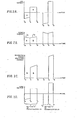
- Figure 2 A is a plot of a. single cycle of current through the gas discharge lamp as a function of time. The current is plotted on the vertical axis and the time is plotted on the horizontal axis. It will be understood that the current alternates through the lamp in a repetitive cycle.'
- the transistor switch 14 is in the off state and the collapsing field in the inductor 17 is forcing a current through the gas discharge lamp.
- the region A covers a period of time between time T 0 and time T A . This time period is equal to the unstable period of - multivibrator 18.
- the transistor switch 14 is on.
- the region B lies between the time T A and the time T B , after which the cycle repeats itself.
- Figure 2 B is a plot of the current through the choke or inductor 17 as a fpnction of time.
- the current through the choke is plotted on the vertical axis, while time is plotted on the horizontal axis.
- A At time T O the transistor has been turned off and the current through the choke is decaying as a function of time until time T A .
- T A At tine T A , the transistor is turned on.
- B The current through the choke in the region of Figure 2B denoted "B" increases until time T B , at which time the transistor is turned back off, and the cycle repeats itself.
- the behavior of the circuit thus alternates between the behavior plotted in region A and the behavior plotted in region B.
- Figure 2C is the plot of the collector current of the transistor plotted as a function of time.
- the collector current amplitude is plotted on the vertical axis and time is plotted on the horizontal axis.
- the transistor is off and therefore the collector current remains zero, from time T O to the end of region A at time T A .
- the collector current In the region deonted B in Figure 2C, at time T A the transistor is turned on and remains on until time T B , which defines the end of region B. During this time, the collector current continually increases.. At time T B the transistor is again turned off and process repeats itself. Thus, the collector current is periodic in time.
- the current level indicated by the plot is equal to the voltage on'the conductor 22 of Figure 1 divided by the resistance of the resistor 15 in Figure 1.
- Figure 2 D is a plot of the voltage across the gas discharge lamp as a function of time. It is identical in shape to the lamp current shown in Figure 2A at the operating frequency of the circuit, i.e. the frequency at which,the transistor switch 14 is switched on and off. iThis frequency is chosen so that its period is short compared to the ionization time of the lamp. A representative operating range is from between 20 to 40 kHz. At this high frequency, the lamp appears electrically to be a resistor. Since the current through a resistor is linearly proportioned to the voltage across it, the lamp voltage and current wave forms are identical in shape.
- the current passing through the resistor, 15 in Figure 1 is the collector current of the transistor. This current is plotted in Figure 2C, as the sum of the lamp current and choke current in region B.
- the peak collector current level is equal to the voltage on the conductor 22 in Figure 1 divided by the resistance of the resistor, 15 in Figure 1.
- the collector current peak level will increase or decrease, respectively.
- the decay time of the current between time TO and time T A is always the same, the minimum value of the collector current will also increase or decrease, respectively.
- the entire waveform of the collector current will be shifted either up or down, respectively, of which two exemplary waveforms are plotted for the two different potentiometer settings "X" and "Y”.
- the waveforms of the choke current and the lamp current will also be shifted up or down, respectively, as shown. This effect is the result of the fact.that the collector current through the transistor is the sum of the choke current and lamp current, and the fact that the lamp current is proportional to the choke current.
- the useful life of the gas discharge lamp is increased in this invention since the net DC component of current through the lamp during continued operation is approximately zero. This is achieved by virtue of the parallel inductance which has the property of maintaining a zero DC voltage drop across its terminals. Since this zero DC voltage is also maintained across the lamp, the DC current through the lamp will also be zero.
- Figure 3 illustrates a modified embodiment in which a gas discharge lamp_ 35, typically a low pressure mercury vapor fluorescent lamp of approximately 22 watts, is provided.
- the electrodes 38 and 40 are of the heated type. Power is derived from a DC voltage source 16.
- An inductor 37 is connected in series with the transistor 14 and resistor 15 across the power supply 36.
- the electrodes 38 and 40 of lamp 35 are tapped into sections 41 and 42 of the winding of inductor 37 to preheat such electrodes prior to ignition of the lamp.
- the inductor 37 also acts as the primary winding of a transformer and has an iron core 39 and a step-down secondary winding 43 associated therewith.
- the winding 43 is connected in circuit with a diode 44 across a capacitor 45.
- the diode 44 is also connected through line 46 to the power input terminals of the comparator amplifier 20 and multivibrator 18. It is also used to supply the reference voltage to the potentiometer 23.
- the sections 41 and 42 of the winding of inductor 37 enable the electrodes 33 and 40 to become heated before the lamp is ignited. This arrangement maximizes electrode life and prevents damage to the electrodes 38 and 40 due to the otherwise excessive rise of temperature at the start of a lamp operation.
- the polarity of the winding 43 is preferably such that the capacitor 45 is charged only when the transistor 14 is conducting. This arrangement ensures that the particular voltage on capacitor 45 is independent of the variable flyback voltage developed'by the inductor 37 when the transistor 14 is cut off.
- the control circuit of Figure 1 is particularly suited for use with low intensity, low pressure mercury vapor fluorescent lamps.
- gas discharge lamps such as high pressure mercury vapor, high or low pressure sodium, and metal Halide lamps, significant problems may arise.
- the common technique for igniting the fluorescent lamp is to connect the secondary winding of a step-up transformer in series with the lamp,-and connect the primary winding to a capacitive discharge device.
- Such a scheme presents insignificant problems in these prior art heavy ballast circuits because the additional inductance of the secondary winding is small compared to the inductance already present in the ballast.
- these prior art 60-Hertz ballast circuits do not fly back, as does a lamp circuit opening at 20-kHz as may a circuit according to the invention. As will be seen in a later portion of this description, the flyback cycle of the lamp control circuit creates special problems when the step-up transformer is introduced.
- Figure 4 illustrates a circuit which provides ' the ignition voltage of 2500 volts in a lamp control circuit similar to the control circuit as illustrated in Figure 1 but using a high voltage ignition circuit similar to that used with prior art lamp ballast circuits.
- the high voltage ignition circuit includes a step-up transformer 950 having a primary winding 951 and a secondary winding 952.
- the secondary winding 952 is connected in series with the gas discharge lamp 11 while the primary winding 951 is connected to a pulse voltage source 953, which may, for example, be a capacitive discharge device.
- Control circuit 949 of Figure 4 includes the control components of Figure 1 including the multivibrator 18, the comparator amplifier 20, the potentiometer 23, and the reference voltage source 24.
- the pulse transformer 950 has a step-up ratio which is sufficient to provide 2500 volts for the lamp 11.
- the capacitive discharge device 953 provides a high voltage pulse to the primary winding 951, which is stepped up by the pulse transformer 950 to approximately 2500 volts across the secondary winding 952. This 2500 volts appears across the lamp 11, and causes the gas inside the lamp 11 to begin to ionize. If the first voltage pulse from the capacitive discharge device 953 is insufficient to completely ignite the lamp, the process will be repeated until ionization in the lamp is complete and the lamp 11 begins to conduct. At this point, the remainder of the control circuit may begin to function as described above in connection with Figures 1 and 2...
- control circuit of Figure 4 has the disadvantage that, after the lamp 11 has ignited, current through the lamp 11 will cause a current to be induced through the primary winding 951 having a large magnitude corresponding to the large step-up ratio of the transformer 950. As a result, a significant power loss will occur through the transformer 950. This will decrease the efficiency of the control circuit of Figure 4 significantly.
- a solution to this problem is to provide a switch 954 which may be opened to prevent current from flowing through the primary winding 951. However, after the switch 954 has been opened, the secondary winding 952 now acts as a large inductor in series with the lamp-in addition to the inductor 17.
- the lamp ballast circuits of the prior-art typically have large inductors, introduction of the secondary winding of the step-up transformer of the ignition circuit did not represent a significant increase in the inductance of the circuit, and therefore, introduction of the high voltage ignition circuit into the prior art.ballast circuits did not change the operation of these circuits significantly.
- the addition of the secondary winding 952 to the 20-kiloHertz lamp control of Figure 4 represents a significant increase in the inductance in the circuit because the inductor 17 is relatively small.
- the 20-kiloHertz control circuit of Figure 1 flies back each 20-kiloHertz cycle.
- the inductance of the secondary winding 952 represents a significant increase in the total inductance of the control circuit of Figure 4, which corresponds to a significant increase in the flyback voltage impressed across the transistor 14 and the varistor 27.
- This increase in flyback voltage causes the varistor 27 to conduct more current to ground during the flyback cycle of the circuit of Figure 4 , representing a further loss'in efficiency of this circuit of Figure 4.
- the circuit of Figure 5 illustrates an embodiment of the invention in which the foregoing - problems are solved.
- the control circuit of Figure 5 includes a lamp control circuit similar to the lamp control circuit of Figure 1, and further includes a pulse transformer 950 having its primary winding 951 connected across a pulse voltage source 953 such as a capacitive discharge device and a secondary winding 952 connected in series with the lamp 11.
- the circuit includes a rectifying diode 955 connected across the secondary winding 952, and a control circuit 956.
- the diode 955 may be any rectifying means, and has its polarity disposed so as to permit current flowing from the inductor 17 to the lamp 11 when the transistor 14 is turned off to flow through the diode 955 and bypass the secondary winding 952 and provides an alternative path for current flowing in the secondary winding 952 during the flyback cycle.
- the diode 955 maintains a substantially constant current through the secondary winding 952 so that the winding 952 does not present any substantial impedance or energy loss during the charging cycle of the circuit. This feature substantially prevents the inductance of the secondary winding 952 from affecting the operation of the lamp control circuit during its normal operating mode after the lamp 11 has been ignited.
- the control circuit 956 controls the operation of the pulsed voltage source 953.
- the control circuit 956 has one of its inputs 956a sensing the other input 956b senses the output fram the control circuit 949 to the base of the transistor 14.
- the control circuit 956 causes the pulsed voltage source 953 to -impose a voltage in the primary winding 951, which is of sufficient magnitude to cause an ignition voltage of 2500 volts on the secondary winding 952. This ignition voltage causes the gas in the lamp 11 to begin ionization. If this ionization is not complete, then during the next cycle of the lamp control circuit the control circuit 956 will again sense that the lamp is still nonconducting by a high collector voltage of the transistor 14 sensed at input 956a.
- the control circuit 956 will reactivate the pulsed voltage source 953 causing the pulse transformer 950 to produce a 2500-volt ignition pulse for a duration determined by the pulsed voltage source 953. This cycle will repeat itself until the lamp 11 has ionized sufficiently to permit a normal driving of the lamp 11 with only the driving circuit 949.
- This circuit has the advantage that, after the lamp 11 is ignited, the inductance of the secondary winding 952 does not affect the operation of the lamp control circuit.
- the operation of the circuit of Figure 5 when the lamp 11 is ignited is as follows: After ignition of the lamp 11, the control circuit of Figure 5 assumes its normal oprating mode similar to that described above in connection with Figures 1 and 2 , and the secondary winding 952 effectively becomes an inductor, as the control circuit 956 opens the primary winding.951 to effectively take it out of the circuit.
- the control circuit 956 opens the primary winding.951 to effectively take it out of the circuit.
- the diode 955 shunts 952, thereby preventing this current from affecting the operation of the control circuit of Figure 5.
- the current through the secondary Winding 952 does not significantly decrease during the flyback cycle. Therefore, when the transistor 14 is again turned back on, the current supplied from the power source 16 flowing through the lamp 11 is not required to significantly change the current flowing through the secondary winding 952.
- current in the secondary winding remains fairly constant and the secondary winding 952 does not present a significant impedance to the current flowing through the lamp 11 during the charging portion of the 20-kiloHertz cycle. Therefore, the secondary winding 952 does not absorb significant power from the power source 16.
- the shunting diode 955 prevents the inductance of the secondary winding 952 from affecting operation of the control circuit of Figure 5 during either the charging portion or the flyback portion of the 20-kiloHertz cycle. Furthermore, because the diode 955 shunts the current across the secondary winding 952 during the flyback cycle, the_inductance of the secondary winding 952 does not contribute to the flyback voltage across the transistor 14. Instead, only the inductor 17 contributes to the flyback voltage across the collector of the transistor 14, as in the circuit of Figure 1, even though the circuit of Figure 5 includes the pulse transformer 950 in series with the lamp 11 having a very high'step-up ratio. This embodiment thus includes a source producing a high ignition voltage across the lamp 11 which does not increase the flyback voltage in the lamp control circuit.
- the lamp 11 in Figure 1 is a high pressure sodium lamp
- the potentiometer 23 of Figure 1 is first adjusted so that the control circuit of Figure 1 furnishes 400 watts of power to the lamp 11
- the voltage drop across the lamp when new would be approximately 95 volts.
- this voltage can increase to 135 volts.
- the control circuit of Figure 1 will increase the lamp voltage, plotted in Figure 2D, so that the current through resistor 15, plotted in Figure 2C, does not change. This voltage increase corresponds to an increase in the power consumed, and a significant increase in the cost of operating the lamp control circuit.
- Figure 6 illustrates another modification of the invention in which the 'foregoing problems are solved.
- the current regulation circuit of Figure 6 comprises another transformer 960 connected in series with lamp 11 in a lamp control circuit similar to the lamp control circuit of Figure 1.
- the transformer 960 has its primary winding 961 connected in series with the lamp. Secondary winding 962 of the transformer 960 is wound to provide a reversed polarity with respect to the primary winding 961, so that the current flowing from the voltage source 16 through the'lamp 11 while the transistor 14 is on produces a negative voltage and reverse current in the secondary winding 962. Isolation diodes 963 and 964 are provided on the ungrounded side of the secondary winding 962.
- the negative voltage in the secondary winding 962 causes a negative voltage to appear across the resistor 965 which is proportional only to the current through the lamp 11.
- Resistors 966 and 967 are connected to form a summing node 968 for the voltage across resistor 965.
- the voltage across the resistor 15 is a function of the current through both the lamp 11 and the inductor 17. This voltage is applied to summing node 968 through summing node resistor 966.
- the negative voltage across resistor 965 is applied to summing node 968 through summing node resistor 967.
- the resistance values of resistors 15,965,966,967 are preferably selected so that the contribution to the voltage across resistor 15 by current through the lamp 11 is precisely nulled at the summing node 968 by the negative voltage across the resistor 965.
- the voltage at the summing node 968 applied to the negative input 20a of the comparator 20 is a function exclusively of the current through inductor 17, and is independent of the current through the lamp 11.
- the comparator amplifier 20 will control the multivibrator 18 and transistor 14 independently of changes in the equivalent resistance of the lamp 11.
- control circuit of Figure 6 does not increase the voltage applied to the lamp 11 as the lamp resistance increases. Therefore, the power consumed by the circuit of Figure 6 will not increase with lamp resistance as does the power consumed by the circuit of Figure 1.
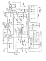
- the lamp control circuit illustrated in the detailed schematic diagram of Figure includes a combination of the features discussed above in connection with Figures 1, 5 and 6.
- the circuit of Figure 7 has a basic lamp control circuit including a gas discharge lamp 11, a switching transistor 14, a resistor 15, a multivibrator 18, and a comparator 20.
- the inductor 17 of Figure 1 is replaced instead by a transformer 970 having primary and'secondary windings 971,972, respectively.
- the transformer 970 transforms the voltage from the voltage source 19 to the optimum operating voltage of the lamp 11.
- the basic lamp circuit including the lamp 11, the transistor 14, and the resistor 15, the multivibrator 18, the comparator 20, the potentiometer 23, and the transformer 970 operate in the manner described above in connection with the lamp control circuit of Figure 1.
- the high ignition voltage circuit of Figure 5 is included in the circuit of Figure 7 as the pulse transformer 950 having its primary minding and to controller 956.
- the diode 955 is connected across the secondary winding 952 in the circuit of Figure 7 and prevents the inductance of the secondary winding 952 from affecting the operation of the basic lamp control circuit, in the same manner as described above in connection with the pulse transformer circuit of Figure 5.
- the controller 956 is preferably a silicon controlled rectifier.
- the gate of the silicon controlled rectifier is connected to the multivibrator circuit 18. When the multivibrator circuit 18 turns the transistor 14 on, it simultaneously causes a voltage at the gate of the silicon controlled rectifier 956 to turn the silicon controlled rectifier 956 on.
- the current regulation circuit described above in connection with Figure 6 is also present in the circuit of Figure 7, and includes the transformer 960 having its primary winding 961 connected in series with the lamp 11, arid its secondary winding 962 wound with opposing polarity and connected through isolation diode 963 to resistor 965.
- Summing node 968 sums the voltage across resistor 15 through summing resistor 966 and the voltage across resistor 965 through summing resistor 967 and applies the resultant voltage to the input 20a of comparator 20.
- This current regulation circuit operates in the same manner described above in connection with the current regulation circuit of Figure 28.
- the circuit of Figure 7 also includes a delay circuit 980 connected to shut-down input 18a of the multivibrator circuit 18.
- the delay circuit 980 shuts down the multivibrator circuit 18 by applying a signal to shut-down input 18a as soon as power is first applied from the voltage source 19 in order to allow the discharge capacitors 953a,953b to have enough time to charge up to a sufficient voltage to ignite lamp 11. After a predetermined length of time, the delay circuit 980 no longer shuts down the multivibrator circuit 18, and the lamp control circuit of Figure 7 begins to operate.
- the metal oxide varistor 27 is connected to the collector transistor 14 in the same manner as described above in connection with Figure 1.
- a second shut-down circuit 990 which shuts down the multivibrator circuit 18 for a predetermined length of time whenever the varistor 27 senses a high enough voltage across transistor 14 to break down.
- the low side of varistor 27 is connected to the input of the protective shut-down circuit 990.
- the output of the second shut-down circuit 990 is connected to the shut-down input 18a of multivibrator circuit 18.
- the second shut-down circuit 990 includes an astable multivibrator 991. Breakdown of the varistor 27 causes the multivibrator 991 to change state and issue a signal to the shut-down input 18, which holds the multivibrator circuit 12 shut down for a predetermined length of time determined by the duration of the astable state of the multivibrator 991.
- This arrangement permits repeated pulses to be produced for starting the lamp if ionization is not complete after the first pulse, by allowing the capacitors 953a and 953b sufficient time to recharge. Again, after the capacitors 953a,953b have recharged, the S.C.R. 95 6 again fires to cause a high voltage pulse across the lamp.
Landscapes
- Circuit Arrangements For Discharge Lamps (AREA)
Applications Claiming Priority (2)
| Application Number | Priority Date | Filing Date | Title |
|---|---|---|---|
| US973613 | 1978-12-27 | ||
| US05/973,613 US4266165A (en) | 1978-12-27 | 1978-12-27 | High intensity discharge lamp starting circuit |
Related Parent Applications (1)
| Application Number | Title | Priority Date | Filing Date |
|---|---|---|---|
| EP79900097.1 Division | 1978-12-28 |
Publications (1)
| Publication Number | Publication Date |
|---|---|
| EP0081863A2 true EP0081863A2 (fr) | 1983-06-22 |
Family
ID=25521060
Family Applications (1)
| Application Number | Title | Priority Date | Filing Date |
|---|---|---|---|
| EP82200903A Withdrawn EP0081863A2 (fr) | 1978-12-27 | 1978-12-28 | Appareil de commande pour faire fonctionner une lampe à décharge |
Country Status (2)
| Country | Link |
|---|---|
| US (1) | US4266165A (fr) |
| EP (1) | EP0081863A2 (fr) |
Cited By (1)
| Publication number | Priority date | Publication date | Assignee | Title |
|---|---|---|---|---|
| GB2201307A (en) * | 1987-02-12 | 1988-08-24 | David John Martin | Electronic starter for discharge lamps |
Families Citing this family (10)
| Publication number | Priority date | Publication date | Assignee | Title |
|---|---|---|---|---|
| US4375608A (en) * | 1980-05-30 | 1983-03-01 | Beatrice Foods Co. | Electronic fluorescent lamp ballast |
| US4716503A (en) * | 1984-09-20 | 1987-12-29 | Fine Lines International Ltd. | Fluorescent display base |
| US4999547A (en) * | 1986-09-25 | 1991-03-12 | Innovative Controls, Incorporated | Ballast for high pressure sodium lamps having constant line and lamp wattage |
| US5041767A (en) * | 1990-03-30 | 1991-08-20 | Bertonee Inc. | Digital controller for gas discharge tube |
| US5036256A (en) * | 1990-06-21 | 1991-07-30 | Gte Products Corporation | Arc discharge ballast suitable for automotive applications |
| US5051665A (en) * | 1990-06-21 | 1991-09-24 | Gte Products Corporation | Fast warm-up ballast for arc discharge lamp |
| US5386181A (en) * | 1992-01-24 | 1995-01-31 | Neon Dynamics Corporation | Swept frequency switching excitation supply for gas discharge tubes |
| JP4724908B2 (ja) * | 2000-09-26 | 2011-07-13 | 岩崎電気株式会社 | Hidランプの点灯回路 |
| SE518667C2 (sv) * | 2001-03-29 | 2002-11-05 | Apra Light Ab | Energibesparande system för tändning, drift och släckning av anslutna gasurladdningslampor. |
| EP1867216A1 (fr) * | 2005-03-22 | 2007-12-19 | Lightech Electronic Industries Ltd. | Circuit d'allumage pour lampe dhi |
Family Cites Families (5)
| Publication number | Priority date | Publication date | Assignee | Title |
|---|---|---|---|---|
| US3569775A (en) * | 1968-08-29 | 1971-03-09 | Burroughs Corp | Apparatus for starting and operating electric discharge devices |
| BE794165A (fr) * | 1972-01-19 | 1973-07-17 | Philips Nv | Dispositif muni d'une lampe a decharge dans le gaz et/ou dans la vapeur |
| US3969652A (en) * | 1974-01-04 | 1976-07-13 | General Electric Company | Electronic ballast for gaseous discharge lamps |
| US3999100A (en) * | 1975-05-19 | 1976-12-21 | Morton B. Leskin | Lamp power supply using a switching regulator and commutator |
| US4162429A (en) * | 1977-03-11 | 1979-07-24 | Westinghouse Electric Corp. | Ballast circuit for accurately regulating HID lamp wattage |
-
1978
- 1978-12-27 US US05/973,613 patent/US4266165A/en not_active Expired - Lifetime
- 1978-12-28 EP EP82200903A patent/EP0081863A2/fr not_active Withdrawn
Cited By (2)
| Publication number | Priority date | Publication date | Assignee | Title |
|---|---|---|---|---|
| GB2201307A (en) * | 1987-02-12 | 1988-08-24 | David John Martin | Electronic starter for discharge lamps |
| GB2201307B (en) * | 1987-02-12 | 1991-05-29 | David John Martin | Electronic starter for discharge lamps |
Also Published As
| Publication number | Publication date |
|---|---|
| US4266165A (en) | 1981-05-05 |
Similar Documents
| Publication | Publication Date | Title |
|---|---|---|
| US4230971A (en) | Variable intensity control apparatus for operating a gas discharge lamp | |
| US4168453A (en) | Variable intensity control apparatus for operating a gas discharge lamp | |
| US5148087A (en) | Circuit for driving a gas discharge lamp load | |
| US4189663A (en) | Direct current ballasting and starting circuitry for gaseous discharge lamps | |
| US4914356A (en) | Controller for gas discharge lamps | |
| US4005335A (en) | High frequency power source for fluorescent lamps and the like | |
| US6479949B1 (en) | Power regulation circuit for high frequency electronic ballast for ceramic metal halide lamp | |
| FI66106B (fi) | Krets foer taendning och begraensning av stroemmen i en gasurladdningslampa | |
| US4132925A (en) | Direct current ballasting and starting circuitry for gaseous discharge lamps | |
| US4356433A (en) | HID Lamp power supply | |
| US5321337A (en) | Ballast having starting current restraint circuitry for preventing a large in-rush current and protection circuitry for preventing damage due to a start-up failure | |
| US4238710A (en) | Symmetry regulated high frequency ballast | |
| US4253046A (en) | Variable intensity control apparatus for operating a gas discharge lamp | |
| GB2045554A (en) | Circuit for operating a discharge lamp | |
| GB2055261A (en) | Inverter circuit | |
| US4719390A (en) | Electronic mains connection device for a gas discharge lamp | |
| US4266165A (en) | High intensity discharge lamp starting circuit | |
| EP0772956A1 (fr) | Montage de circuit | |
| US5422545A (en) | Closed loop feedback control circuits for gas discharge lamps | |
| US4376911A (en) | Circuit system for lighting a discharge lamp or lamps | |
| US5530321A (en) | Power supply for a gas discharge lamp | |
| US4853598A (en) | Fluorescent lamp controlling | |
| US4492897A (en) | Means for limiting and controlling the current of a discharge lamp | |
| JP2000348884A (ja) | 電極高圧放電ランプを始動および作動する方法および回路装置 | |
| JPH0119238B2 (fr) |
Legal Events
| Date | Code | Title | Description |
|---|---|---|---|
| PUAI | Public reference made under article 153(3) epc to a published international application that has entered the european phase |
Free format text: ORIGINAL CODE: 0009012 |
|
| AC | Divisional application: reference to earlier application |
Ref document number: 16756 Country of ref document: EP |
|
| AK | Designated contracting states |
Designated state(s): CH DE FR GB LU SE |
|
| STAA | Information on the status of an ep patent application or granted ep patent |
Free format text: STATUS: THE APPLICATION HAS BEEN WITHDRAWN |
|
| 18W | Application withdrawn |
Withdrawal date: 19840327 |
|
| RIN1 | Information on inventor provided before grant (corrected) |
Inventor name: HANDLER, HOWARD |