EP0082652A2 - Circuit mélangeurpour signaux video - Google Patents
Circuit mélangeurpour signaux video Download PDFInfo
- Publication number
- EP0082652A2 EP0082652A2 EP82306619A EP82306619A EP0082652A2 EP 0082652 A2 EP0082652 A2 EP 0082652A2 EP 82306619 A EP82306619 A EP 82306619A EP 82306619 A EP82306619 A EP 82306619A EP 0082652 A2 EP0082652 A2 EP 0082652A2
- Authority
- EP
- European Patent Office
- Prior art keywords
- signal
- signals
- circuit
- sampling
- mixing circuit
- Prior art date
- Legal status (The legal status is an assumption and is not a legal conclusion. Google has not performed a legal analysis and makes no representation as to the accuracy of the status listed.)
- Granted
Links
Images


Classifications
-
- H—ELECTRICITY
- H04—ELECTRIC COMMUNICATION TECHNIQUE
- H04N—PICTORIAL COMMUNICATION, e.g. TELEVISION
- H04N25/00—Circuitry of solid-state image sensors [SSIS]; Control thereof
- H04N25/40—Extracting pixel data from image sensors by controlling scanning circuits, e.g. by modifying the number of pixels sampled or to be sampled
- H04N25/44—Extracting pixel data from image sensors by controlling scanning circuits, e.g. by modifying the number of pixels sampled or to be sampled by partially reading an SSIS array
- H04N25/447—Extracting pixel data from image sensors by controlling scanning circuits, e.g. by modifying the number of pixels sampled or to be sampled by partially reading an SSIS array by preserving the colour pattern with or without loss of information
-
- H—ELECTRICITY
- H04—ELECTRIC COMMUNICATION TECHNIQUE
- H04N—PICTORIAL COMMUNICATION, e.g. TELEVISION
- H04N25/00—Circuitry of solid-state image sensors [SSIS]; Control thereof
- H04N25/10—Circuitry of solid-state image sensors [SSIS]; Control thereof for transforming different wavelengths into image signals
Definitions
- This invention relates to a mixing circuit for mixing sampled signals and, more particularly, to a mixing circuit for mixing together a plurality of sampled outputswhich differ in phase by 2 ⁇ /N from one another.
- An image sensor consisting of a solid-state image sensor element such as a charge coupled device (CCD) generally has a scattered picture element structure.
- CCD charge coupled device
- sensor outputs corresponding to individual picture elements are subjected to a sampling treatment before various signal processings are carried out.
- a luminance signal is formed from a color image output obtained from a solid-state color image sensor provided with a color coding filter
- color signals obtained as a result of color separation of the color image signal are converted through a 1H delay circuit into simultaneous signals, which are additively synthesized in predetermined proportions to obtain the luminance signal.
- the luminance signal Y is defined by an equation That is, the luminance signal Y can be obtained by additively synthesizing blue, green and red signals B, G and R in the proportions 0.11 : 0.59 : 0.30
- the luminance signal Y is formed from a color image output of a solid-state image sensor of a scattered picture element structure
- the turn-round distortion of side bands due to sampling is removed by forming a low frequency luminance component Y L given by and a high frequency luminance component Y H given by and combining these components Y L and Y H to obtain the luminance signal Y.
- an NTSC television signal is formed with a signal processing circuit having a construction as shown in Fig. 2.
- a solid-state color image sensor designated at 1 is a solid-state color image sensor.
- the image sensor 1 is formed as an interline transfer type CCD provided with the color coding filter C F as described above.
- the image sensor 1 provides a color image output at a clock frequency of 2f c .
- the color image output of the image sensor 1 is coupled through a buffer amplifier 2 to a color separating circuit 3.
- the color separating circuit 3 consists of two sample/hold circuits 3A and 3B.
- the sample/hold circuits 3A and 3B are operated under the control of respective sampling clocks which have a frequency f C and are 180° (i.e. ⁇ ) out of phase with each other.
- the sample/hold circuit 3A samples and holds the green signal G in the color image output.
- the other sample/hold circuit 3B samples and holds a red/blue signal R/B.
- Designated at 4 is a white balance control circuit, which includes a fixed gain amplifier 4G for amplifying the G signal, a variable gain amplifier 4R for amplifying the R signal and a variable gain amplifier 4B for amplifying the B signal. The white balance control is done by controlling the gains of the variable gain amplifiers 4R and 4B such that the R, G and B signals are at an equal level.
- Designated at 10 is a luminance signal forming circuit. The G and R/B signals, having been level adjusted in the white balance control circuit 4, are coupled through respective gamma correction circuits 5A and 5B to the luminance signal forming circuit 10.
- the luminance signal forming circuit 10 includes a first signal processing circuit 11 for effecting additive synthesis of the equation (2), a second signal processing circuit 12 for effecting additive synthesis of the equation (3), a low-pass filter 13 for receiving the synthesized output signal of the first signal processing circuit 11, a band-pass filter 14 for receiving the synthesized output signal of the second signal processing circuit 12, and a signal adder 15 for effecting additive synthesis of a low frequency luminance signal Y L obtained from the low-pass filter 13 and a high frequency luminance signal Y H obtained from the band-pass filter 14.
- the three primary color signals R, G and-B-having been gamma corrected in the gamma correction circuits 5A and 5B and the luminance signal Y formed by the luminance signal synthesizing circuit 10 are supplied to a color coder 8.
- the color coder 8 forms a composite video signal according to the NTSC system.
- the second signal processing circuit 12 for forming the high frequency luminance signal Y H has a construction as shown in Fig. 3.
- the G and R/B signals obtained through color separation of the color image signal from the solid-state color image sensor 1 are converted to simultaneous signals through four 1H delay circuits 32, 34, 42 and 44 providing a delay time equal to one horizontal scanning period 1H.
- These simultaneous signals are weightedly added in first and second signal adders 51 and 52 to produce respective addition output signals Y H1 and Y H2 .
- the addition output signals Y H1 and Y H2 are purely added together in a third signal adder 53 to form the high frequency luminance signal Y H .
- the G signal is supplied to a first signal input terminal 21.
- the first signal input terminal 21 is connected through a first sample/hold circuit 31 to a first 1H delay circuit 32.
- the first 1H delay circuit 32 is connected through a second sample/hold circuit 34 to a second 1H delay circuit 34.
- the second IH delay circuit 34 is connected to a third sample/hold circuit 35.
- the R/B signal is supplied to a second input signal terminal 22.
- the second signal input terminal 22 is connected through a sample/ hold circuit 41, a 1H delay circuit 42, a sample/hold circuit 43 a 1H delay circuit 44 and a sample/hold circuit 45.
- the output signals (R/B) 0 and (R/B) 2 from the respective first and third sample/hold circuits 41 and 45 in the R/B signal line and the output signal G 1 from the second sample/hold circuit 33 in the G signal line are coupled through respective weighting circuits 46, 48 and 37 for being weighted such that they are in proportions of 1.(R/B) 0 : 1 ⁇ (R/B) 2 . 2 ⁇ G 1 .
- the signals weighted in these proportions are fed to a first signal adder 51.
- the output signals Go and G 2 from the first and third sample/hold circuits 31 and 35 in the G signal line and the output (R/B) 2 from the second sample/hold circuit 43 in the R/B signal line are weighted in respective weighting circuits 36, 38 and 47 in proportions of 1-G 0 : 1-G 2 : 2.(R/B) 1 . These weighted signals are fed to a second adder 52.
- the sampling and holding operation of the first and third sample/hold circuits 41 and 45 in the R/B signal line and the second sample/hold circuit 33 in the G signal line are done under the control of a clock signal ⁇ 1 .
- the sampling and holding operation of the second sample/hold circuit 43 of the R/B signal line and the first and third sample/hold circuits 31 and 35 in the G signal line are done under the control of a second clock signal ⁇ 2 180 degrees out of phase with the first clock signal 2.
- the transfer function H O (w) has a frequency characteristic as shown by the dashed curve in Figure 4.
- the present invention provides a mixing circuit for mixing at least two sampled input signals comprising:
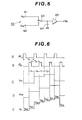
- Fig. 5 shows the basic construction of the sampled signal mixing circuit 60 according to the present invention.
- sampled output signals Y Hl and Y H2 which are 180 degrees out of phase with each other are switched through an analog switch 63 to be supplied to a common holding capacitor 64 for mixing.
- the operational principles of the circuit of Fig. 5 will now be described in connection with the case where the circuit is used as the third signal adder 53 in the signal processing circuit 20 in the luminance signal forming circuit 10 described above.
- the output signals Y H1 and Y H2 from the first and second signal adders 51 and 52 in the signal processing circuit 20 are supplied to the first and second signal input terminals 61 and 62.
- These output signals Y H1 and Y H2 are switched through the analog switch 63 such that they are selectively supplied in respective periods T1 and T 2 which together constitute the sampling period T c to the holding capacitor 64. Since the signals Y H1 and Y H2 have been sampled and held under the control of the clock signals ⁇ 1 and ⁇ 2 which are 180 degrees out of-phase with each other as shown in A and B in Fig. 6, they have waveforms as shown in C and D in Fig. 6.
- Fig. 7 shows a specific circuit construction of the signal mixing circuit 60.
- the circuit 60 includes input buffer transistors 60A and 60B, an output buffer transistor 65' and switching transistors 63A and 63B constituting the analog switch 63.
- the mixing operation as described above is effected in the holding capacitor 64 under the control of gate signals g 1 and g 2 , which have respective pulse widths T 1 and T 2 and a repetition period T c and are supplied to the gates of the respective switching transistors 63A and 63B.
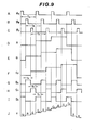
- Fig. 8 shows a different embodiment of the invention.
- signals sampled 2 ⁇ /3 out of phase with one another are mixed together as in the case of forming luminance signal Y by mixing together color signals R , G and Cy obtained through color disassembly of a color image output of a frame transfer type CCD image sensor provided with vertical stripes color filters for red (R), green (G) and cyan (C Y ).
- R, G and C Y signals as shown in D, E and F in Fig. 9, which are obtained by color disassembly under the control of clock signals ⁇ A , ⁇ B and ⁇ C ,2 ⁇ /3 out of phase with one another as shown at A, B and C in Fig.
- the R, G and C Y signals are coupled through input buffer transistors 74, 75 and 76 to switching transistors 77, 78'and 79 for analog switching to be selectively supplied to a holding capacitor 80.
- the first switching transistor 77 operates under the control of a gate signal g x as shown at G in Fig. 9, synchronized to the sampling clock signal ⁇ A for the G signal and having a pulse width T X , and supplies the R signal to the holding capacitor 80 during the period T X .
- the second switching transistor 78 operates under the control of a gate signal g y as shown at H in Fig.
- the third switching transistor 79 operates under the control of a gate signal g z as shown in I at Fig. 9, synchronized to the sampling clock signal ⁇ C for the R signal and having a pluse width T Z , and supplies the R signal to the holding capacitor 80 during the period T Z .
- the pulse periods T X , Ty and T Z of the gate signals g , g and g are set to be equal to one-third of the period T C of the clock signals ⁇ A' ⁇ B and ⁇ C . From the holding capacitor 80, to which the R, G and C Y signals are supplied through switching by the switching transistors 77, 78 and 79, a luminance signal Y as shown in J in Fig. 9 can be obtained via an output buffer transistor 81.
- the transfer function H T (w) given to the luminance signal Y in this embodiment can-be expressed as
- the transfer function H T (w) has a frequency characteristic as shown by the dot-and-bar curve in Fig. 4.
- the sampled outputs may be sequentially supplied through an N-contact analog switch circuit to a common holding capacitor for mixing.
Landscapes
- Engineering & Computer Science (AREA)
- Multimedia (AREA)
- Signal Processing (AREA)
- Color Television Image Signal Generators (AREA)
- Mobile Radio Communication Systems (AREA)
- Input Circuits Of Receivers And Coupling Of Receivers And Audio Equipment (AREA)
- Stereo-Broadcasting Methods (AREA)
- Processing Of Color Television Signals (AREA)
- Control Of Motors That Do Not Use Commutators (AREA)
Priority Applications (1)
| Application Number | Priority Date | Filing Date | Title |
|---|---|---|---|
| AT82306619T ATE29096T1 (de) | 1981-12-11 | 1982-12-10 | Mischschaltung fuer videosignale. |
Applications Claiming Priority (2)
| Application Number | Priority Date | Filing Date | Title |
|---|---|---|---|
| JP199858/81 | 1981-12-11 | ||
| JP56199858A JPS58100590A (ja) | 1981-12-11 | 1981-12-11 | サンプリング出力の合成方法 |
Publications (3)
| Publication Number | Publication Date |
|---|---|
| EP0082652A2 true EP0082652A2 (fr) | 1983-06-29 |
| EP0082652A3 EP0082652A3 (en) | 1984-12-05 |
| EP0082652B1 EP0082652B1 (fr) | 1987-08-19 |
Family
ID=16414816
Family Applications (1)
| Application Number | Title | Priority Date | Filing Date |
|---|---|---|---|
| EP82306619A Expired EP0082652B1 (fr) | 1981-12-11 | 1982-12-10 | Circuit mélangeurpour signaux video |
Country Status (6)
| Country | Link |
|---|---|
| US (1) | US4527190A (fr) |
| EP (1) | EP0082652B1 (fr) |
| JP (1) | JPS58100590A (fr) |
| AT (1) | ATE29096T1 (fr) |
| CA (1) | CA1194988A (fr) |
| DE (1) | DE3277052D1 (fr) |
Cited By (1)
| Publication number | Priority date | Publication date | Assignee | Title |
|---|---|---|---|---|
| CN108074528A (zh) * | 2016-11-17 | 2018-05-25 | 乐金显示有限公司 | 显示装置及其控制器 |
Families Citing this family (8)
| Publication number | Priority date | Publication date | Assignee | Title |
|---|---|---|---|---|
| DE3344082A1 (de) * | 1982-12-07 | 1984-06-07 | Canon K.K., Tokio/Tokyo | Bildaufnahme-einrichtung |
| KR900003267B1 (ko) * | 1984-10-06 | 1990-05-12 | 니뽕 빅터 가부시끼가이샤 | 칼라 촬상 장치 |
| US4814861A (en) * | 1985-07-10 | 1989-03-21 | Canon Kabushiki Kaisha | Signal processing apparatus with independent gain control for chrominance and color signals |
| JP2595207B2 (ja) * | 1986-01-29 | 1997-04-02 | 富士写真フイルム株式会社 | 映像信号の形成装置 |
| JPH0681319B2 (ja) * | 1987-02-14 | 1994-10-12 | 日本放送協会 | 電子画像エンコ−ダ |
| JPH07110065B2 (ja) * | 1987-05-01 | 1995-11-22 | 富士写真フイルム株式会社 | デイジタル電子スチルカメラ |
| JPH0851635A (ja) * | 1994-08-05 | 1996-02-20 | Sony Corp | 撮像装置 |
| US7375664B2 (en) * | 2006-06-07 | 2008-05-20 | Texas Instruments Incorporated | Systems and methods for providing anti-aliasing in a sample-and-hold circuit |
Family Cites Families (4)
| Publication number | Priority date | Publication date | Assignee | Title |
|---|---|---|---|---|
| US4059838A (en) * | 1976-09-24 | 1977-11-22 | General Electric Company | Chroma-preference control for VIR automatic operation |
| CA1089981A (fr) * | 1977-06-29 | 1980-11-18 | Takao Tsuchiya | Circuit de calage pour signaux de television en couleurs |
| JPS5437533A (en) * | 1977-08-30 | 1979-03-20 | Sony Corp | Color pickup unit |
| JPS5690689A (en) * | 1979-12-24 | 1981-07-22 | Sony Corp | Signal processing circuit for dot-sequential image pickup output signal |
-
1981
- 1981-12-11 JP JP56199858A patent/JPS58100590A/ja active Granted
-
1982
- 1982-12-09 US US06/448,408 patent/US4527190A/en not_active Expired - Lifetime
- 1982-12-09 CA CA000417383A patent/CA1194988A/fr not_active Expired
- 1982-12-10 DE DE8282306619T patent/DE3277052D1/de not_active Expired
- 1982-12-10 EP EP82306619A patent/EP0082652B1/fr not_active Expired
- 1982-12-10 AT AT82306619T patent/ATE29096T1/de not_active IP Right Cessation
Cited By (1)
| Publication number | Priority date | Publication date | Assignee | Title |
|---|---|---|---|---|
| CN108074528A (zh) * | 2016-11-17 | 2018-05-25 | 乐金显示有限公司 | 显示装置及其控制器 |
Also Published As
| Publication number | Publication date |
|---|---|
| DE3277052D1 (en) | 1987-09-24 |
| ATE29096T1 (de) | 1987-09-15 |
| EP0082652A3 (en) | 1984-12-05 |
| JPH0470828B2 (fr) | 1992-11-12 |
| EP0082652B1 (fr) | 1987-08-19 |
| CA1194988A (fr) | 1985-10-08 |
| JPS58100590A (ja) | 1983-06-15 |
| US4527190A (en) | 1985-07-02 |
Similar Documents
| Publication | Publication Date | Title |
|---|---|---|
| EP0660617B1 (fr) | Dispositif de prise d'image | |
| US5262849A (en) | Digital camera processing device having variably settable interpolation | |
| JPH04269091A (ja) | カラーテレビジョンカメラ装置 | |
| KR920001009B1 (ko) | 촬상장치 | |
| JP3035930B2 (ja) | カラー固体撮像装置 | |
| US5184212A (en) | Circuit for producing brightness signal from output signal of solid state image pick-up apparatus using spatial pixel shift | |
| EP0082652B1 (fr) | Circuit mélangeurpour signaux video | |
| US4827331A (en) | Color TV camera with circuit for adjusting the white balance of red, green, and blue signals generated from a narrow-band luminance signal and line-sequential color-difference signals | |
| KR950001577B1 (ko) | 색분리 및 윤곽 보정회로 | |
| EP0507450B1 (fr) | Appareil de caméra de télévision en couleur numérique | |
| EP0624041B1 (fr) | Caméra vidéo couleur | |
| GB2103051A (en) | Sample/hold circuit arrangements | |
| US5349381A (en) | Video camera with aperture correction having reduced power consumption | |
| JPH0884348A (ja) | 撮像装置 | |
| KR960016442B1 (ko) | 고체촬상소자를 갖는 비디오카메라 | |
| US5124786A (en) | Color signal enhancing cirucit for improving the resolution of picture signals | |
| EP0068811B1 (fr) | Caméras numériques de couleur | |
| US7688362B2 (en) | Single sensor processing to obtain high resolution color component signals | |
| US4680623A (en) | Solid state color imaging apparatus producing chrominance and luminance signals from unsaturated ores of n color signals | |
| JP3131127B2 (ja) | 撮像装置の信号処理回路 | |
| JPH0223076B2 (fr) | ||
| JPS6229388A (ja) | カラ−固体撮像装置 | |
| JPH0530429A (ja) | 固体撮像素子の信号処理回路 | |
| JP2922911B2 (ja) | 固体カラーカメラ | |
| EP0485221A2 (fr) | Dispositif de prise d'images à l'état solide ayant un filtre couleur |
Legal Events
| Date | Code | Title | Description |
|---|---|---|---|
| PUAI | Public reference made under article 153(3) epc to a published international application that has entered the european phase |
Free format text: ORIGINAL CODE: 0009012 |
|
| AK | Designated contracting states |
Designated state(s): AT DE FR GB NL |
|
| PUAL | Search report despatched |
Free format text: ORIGINAL CODE: 0009013 |
|
| AK | Designated contracting states |
Designated state(s): AT DE FR GB NL |
|
| 17P | Request for examination filed |
Effective date: 19850301 |
|
| 17Q | First examination report despatched |
Effective date: 19860320 |
|
| GRAA | (expected) grant |
Free format text: ORIGINAL CODE: 0009210 |
|
| AK | Designated contracting states |
Kind code of ref document: B1 Designated state(s): AT DE FR GB NL |
|
| REF | Corresponds to: |
Ref document number: 29096 Country of ref document: AT Date of ref document: 19870915 Kind code of ref document: T |
|
| ET | Fr: translation filed | ||
| REF | Corresponds to: |
Ref document number: 3277052 Country of ref document: DE Date of ref document: 19870924 |
|
| PLBE | No opposition filed within time limit |
Free format text: ORIGINAL CODE: 0009261 |
|
| STAA | Information on the status of an ep patent application or granted ep patent |
Free format text: STATUS: NO OPPOSITION FILED WITHIN TIME LIMIT |
|
| 26N | No opposition filed | ||
| PGFP | Annual fee paid to national office [announced via postgrant information from national office to epo] |
Ref country code: GB Payment date: 20011212 Year of fee payment: 20 Ref country code: FR Payment date: 20011212 Year of fee payment: 20 Ref country code: AT Payment date: 20011212 Year of fee payment: 20 |
|
| PGFP | Annual fee paid to national office [announced via postgrant information from national office to epo] |
Ref country code: NL Payment date: 20011228 Year of fee payment: 20 |
|
| REG | Reference to a national code |
Ref country code: GB Ref legal event code: IF02 |
|
| PGFP | Annual fee paid to national office [announced via postgrant information from national office to epo] |
Ref country code: DE Payment date: 20020109 Year of fee payment: 20 |
|
| PG25 | Lapsed in a contracting state [announced via postgrant information from national office to epo] |
Ref country code: GB Free format text: LAPSE BECAUSE OF EXPIRATION OF PROTECTION Effective date: 20021209 |
|
| PG25 | Lapsed in a contracting state [announced via postgrant information from national office to epo] |
Ref country code: NL Free format text: LAPSE BECAUSE OF EXPIRATION OF PROTECTION Effective date: 20021210 Ref country code: AT Free format text: LAPSE BECAUSE OF EXPIRATION OF PROTECTION Effective date: 20021210 |
|
| REG | Reference to a national code |
Ref country code: GB Ref legal event code: PE20 Effective date: 20021209 |
|
| NLV7 | Nl: ceased due to reaching the maximum lifetime of a patent |
Effective date: 20021210 |