EP0083031A2 - Dispositif de mémoire à semi-conducteur ayant un circuit de programmation - Google Patents
Dispositif de mémoire à semi-conducteur ayant un circuit de programmation Download PDFInfo
- Publication number
- EP0083031A2 EP0083031A2 EP82111666A EP82111666A EP0083031A2 EP 0083031 A2 EP0083031 A2 EP 0083031A2 EP 82111666 A EP82111666 A EP 82111666A EP 82111666 A EP82111666 A EP 82111666A EP 0083031 A2 EP0083031 A2 EP 0083031A2
- Authority
- EP
- European Patent Office
- Prior art keywords
- mosfet
- memory
- fuse
- flip
- output
- Prior art date
- Legal status (The legal status is an assumption and is not a legal conclusion. Google has not performed a legal analysis and makes no representation as to the accuracy of the status listed.)
- Granted
Links
- 239000004065 semiconductor Substances 0.000 title claims abstract description 45
- 239000003990 capacitor Substances 0.000 claims abstract description 22
- 229910021420 polycrystalline silicon Inorganic materials 0.000 claims abstract description 17
- 229920005591 polysilicon Polymers 0.000 claims abstract description 17
- 230000002950 deficient Effects 0.000 claims description 22
- 238000005224 laser annealing Methods 0.000 claims description 4
- 230000002401 inhibitory effect Effects 0.000 claims description 2
- 230000003111 delayed effect Effects 0.000 abstract 1
- 239000000872 buffer Substances 0.000 description 7
- 238000000034 method Methods 0.000 description 5
- 238000010586 diagram Methods 0.000 description 2
- 230000004048 modification Effects 0.000 description 2
- 238000012986 modification Methods 0.000 description 2
- 230000005540 biological transmission Effects 0.000 description 1
- 230000008878 coupling Effects 0.000 description 1
- 238000010168 coupling process Methods 0.000 description 1
- 238000005859 coupling reaction Methods 0.000 description 1
- 230000000694 effects Effects 0.000 description 1
- XUFQPHANEAPEMJ-UHFFFAOYSA-N famotidine Chemical compound NC(N)=NC1=NC(CSCCC(N)=NS(N)(=O)=O)=CS1 XUFQPHANEAPEMJ-UHFFFAOYSA-N 0.000 description 1
- 239000002784 hot electron Substances 0.000 description 1
- 230000007257 malfunction Effects 0.000 description 1
- 238000004519 manufacturing process Methods 0.000 description 1
- 239000011159 matrix material Substances 0.000 description 1
Images




Classifications
-
- G—PHYSICS
- G11—INFORMATION STORAGE
- G11C—STATIC STORES
- G11C29/00—Checking stores for correct operation ; Subsequent repair; Testing stores during standby or offline operation
- G11C29/70—Masking faults in memories by using spares or by reconfiguring
- G11C29/78—Masking faults in memories by using spares or by reconfiguring using programmable devices
- G11C29/785—Masking faults in memories by using spares or by reconfiguring using programmable devices with redundancy programming schemes
-
- G—PHYSICS
- G11—INFORMATION STORAGE
- G11C—STATIC STORES
- G11C29/00—Checking stores for correct operation ; Subsequent repair; Testing stores during standby or offline operation
- G11C29/70—Masking faults in memories by using spares or by reconfiguring
- G11C29/78—Masking faults in memories by using spares or by reconfiguring using programmable devices
- G11C29/83—Masking faults in memories by using spares or by reconfiguring using programmable devices with reduced power consumption
Definitions
- This invention relates to semiconductor devices and more particularly to semiconductor devices utilizing redundancy techniques.
- semiconductor devices particularly semiconductor memory devices comprise a spare device in addition to a normal device.
- semiconductor devices utilizing redundancy techniques have been increasingly applied.
- the semiconductor memory which utilizes a redundancy technique comprises spare memory cells in addition to normal memory cells.
- a semiconductor memory device even if only one bit is defective, is generally regarded as a substandard device.
- memory devices increase in capacity, defective memory cells tend to occur at a greater frequency. If, in such a case, a memory device in discarded, even though only one bit is found to be defective, the semiconductor memory device would be manufactured with a low yield and at a high cost.
- Fig. l A indicates the arrangement of a conventional programming element.
- a polysilicon fuse 10 is connected between a power supply terminal VDD and an output terminal OUT.
- an enhancement mode MOSFET 12 for programming (unless noted otherwise, the MOSFET is chosen to be an N-channel type) and a depletion mode MOSFET 14.
- a programming signal P is supplied to the gate of the MOSFET 12, and the gate of the MOSFET 14 is grounded.
- binary data is programmed by the blown or connected condition of the polysilicon fuse 10.
- a programming signal P has a logic level "1”
- the MOSFET 12 is rendered conductive, causing current to flow through the fuse 10.
- the fuse 10 is blown by the released Joul heat.
- the output terminal OUT is set at a logic level "0" through the MOSFET 14.
- the MOSFET 12 is rendered nonconductive preventing the fuse 10 from being blown.
- the output terminal OUT is set at a logic level "1" by the ratio between the resistances of the fuse 10 and MOSFET 14.
- Fig. 1B indicates the arrangement of another conventional programming element which produces an output signal having a different level from Fig. lA.
- Fig. 1B when the fuse 10 is blown, an output signal has a logic level "1".
- an output signal When the fuse 10 is connected, an output signal has a logic level "0".
- this invention provides a semiconductor device which comprises a memory element, in which an impedance prevailing across both terminals is set at a first and second level in a nonvolatile state, and a switching element, both elements being connected in series between first and second power supply terminals, and a control circuit which supplies an output signal from the junction of the memory element and switching element to a control terminal of the switching element through a delay element.
- FIG. 2 is a block diagram of a semiconductor memory device according to a first embodiment of the present invention.
- the respective blocks of Fig. 2 are formed on a single chip.
- a memory cell unit 20 comprises normal memory cells 22 and spare memory cells 24.
- the normal _ memory cells 22 are arranged in the matrix form and the spare memory cells 24 correspond to several rows of the normal memory cells 22, and the replacement of normal memory cells by spare memory cells is effected for each row.
- a column address signal is supplied to a column address buffer 26, and a row address signal is supplied to a row address buffer 28.
- the address buffers 26 and 28 send forth an address signal and its inverted signal.
- An output signal from the column address buffer 26 is delivered to a column decoder 30, which in turn selects one column from among a plurality of memory cell columns.
- An output signal from the row address buffer 28 is supplied to a normal row decoder 32.
- An output signal from the normal row decoder 32 is sent forth to each row of the normal memory cells 22.
- An output signal from the row address buffer 28 is also supplied to a programming circuit 34 whose output signal is supplied to a spare row decoder 36.
- An output signal from a spare row decoder 36 is delivered to each row of the spare memory cells 24.
- An output signal from the spare row decoder 36 is also supplied to the normal row decoder 32 as a decoding- inhibiting signal.
- the spare row decoder 36 is formed of decoder units having the same number as the rows of the spare memory cells. An output signal from each row decoder unit is supplied to the corresponding row of spare memory cells.
- the programming circuit 34 consists of a plurality of programming units corresponding to the respective decoder units.
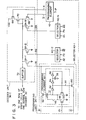
- Fig. 3 indicates a programming unit 34-1 and a decoder unit 36-1. Now let it be assumed that a row address signal is of N bit. Then the programming unit 34-1 is chosen to comprise N selectors 40-1 to 40-N, and a programming element 42. This programming element 42 is the very unit on which this invention is fundamentally based.
- the selectors 40-1 to 40-N respectively include programming elements 44-1 to 44-N. However, it is unnecessary, as later described, to provide the programming element 42 which is not included in selectors 40-1 to 40-N.
- a polysilicone fuse 46 is connected at one end to the power supply terminal VDD and at the other end is grounded through parallel-connected MOSFETs 48 and 50 (unless otherwise noted, the MOSFET is assumed to have an enhancement mode of the N-channel type).
- gate of the MOSFET 48 is supplied with a programming signal P.
- the fuse 46 is connected at the other end to a program output signal line X and also to the gate of the MOSFET 50 through series-connected inverters 52, 54 and 56.
- a junction between the inverters 54 and 56 is grounded through a capacitor 58.
- the inverter 54 and capacitor 58 jointly constitute a delay circuit.
- An output terminal of the inverter 52 is connected to another program output signal line X.
- the selector 40 is formed of a programming element 44 constructed as described above, and MOSFETs 60 and 62 whose gates are respectively connected to the program output signal lines X and X.
- the MOSFETs 60 and 62 are respectively supplied at one end with address signals A and A, and at the other end are jointly connected to an output line B.
- an output line B of the selector 40 is supplied with an address signal A or A, depending on the physical condition of the fuse 46.
- Either output signal X or X from a programming element 42 or 44 is chosen to have a logic level "1", depending on the physical condition of the fuse 46.
- Output signals Bl to BN from the selectors 40-1 to 40-N are respectively delivered to the gates of MOSFETs 64-1 to 64-N included in the decoder unit 36-I.
- Output signals X and X of the programming element 42 are respectively delivered to the gates of MOSFETs 66 and 68.
- the MOSFET 66 is connected at one end to the power source terminal VDD and at the other end is grounded through series-connected depression mode MOSFET 70 and the MOSFET 68.
- MOSFETs 64-1 to 64-N are connected in parallel between the junction of the MOSFETs 70 and 68 and the ground.
- the gate of the MOSFET 70 is connected to the junction of the MOSFETs 70 and 68.
- a signal from the junction of the MOSFETs 70 and 68 is delivered through a buffer 72 to one row of the spare memory cells 24 and to the normal row decoder 32.
- the normal row decoder 32 (not shown) is constructed in the same manner as the spare row decoder 36.
- an output signal is chosen to have a logic level "0".
- an output signal from the inverter 56 that is, the gate of the MOSFET 50 is held at a logic level "1" for a prescribed length of time after power is supplied.
- the MOSFET 50 is rendered conductive when power is supplied.
- the junction of the fuse 46 and MOSFET 48 is reliably set at a logic level "0".
- the logic level "1" is transmitted through the inverters 52 and 54 to the inverter 56.
- the length of time required for the transmission is defined to fall within the prescribed period of time during which the input .terminal potential of the inverter 56 is set at a logic level "0" due to the capacitor 58.
- the input terminal of the inverter 56 is always set at a logic level "0".
- an output signal from the inverter 56 has a logic level "1", causing the MOSFET 50 to be rendered conductive.
- the output signals X and X respectively have logic levels "1" and "0".
- the junction of the fuse 46 and MOSFET 48 is at a logical level "1”.
- the resistance of the fuse 46 and MOSFET 50 is so defined as to cause the junction of the fuse 46 and MOSFET 50 to be set at a logic level "1".
- the fuse 46 is prevented from being blown by mistake, thereby increasing the reliability of data programmed in the programming elements 42 and 44.
- the MOSFETs 48 and 50 are rendered nonconductive. Therefore, the junction of the fuse 46 and MOSFET 50 is brought to an electrically floating state. Since the potentials of the respective junctions are defined when power is supplied, the junction of the fuse 46 and MOSFET 50 undesirably tends to have its potential raised to a logic level "1" or is rendered unstable due to the capacitive coupling between the junction of the fuse 46 and MOSFET 50 and any other nodes which might rise to a logic level "1" or due to the occurrence of noise when power is supplied.
- the voltage of the output signals X and X from the programming element 42 are respectively set at logic levels "1" and "0".
- the MOSFETs 66 and 68 included in the decoder unit 36-1 are respectively rendered conductive and nonconductive. In other words, when one row of the spare memory cells 24 is used, the fuse of the programming element 42 is first blown.
- the programming signal PI is set at a logic level "0".
- the row "010" of the normal memory cells is assumed to contain a defective bit. Therefore, a programming signal P2 supplied to the selector 40-2 is set at a logic level "1".
- the output signals X and X from the programming element 44-2 included in the selector 40-2 are respectively set at logic levels "1” and "0", causing the MOSFETs 60 and 62 to be respectively rendered conductive and nonconductive. Consequently, an input signal A2 is selected and the selector 40-2 sends forth an input signal A2 as an output signal B2.
- Programming signals Pl and P3 supplied to the other selectors 40-1 and 40-3 are set at a logic level "0".
- the selectors 40-1 and 40-3 respectively issue the input signals Al and A3 as output signals Bl and B3.
- the output signals Bl, B2 and B3 from the respective selectors 40-1, to 40-2 and 40-3 are the signals Al, A2 and A3, respectively.
- the row address signal becomes "010”
- the output signals from the programming unit 34-1 are all "0".
- the programming unit 34-1 is so programmed as to cause all of the output signals to be set at a logic level "0".
- the transistors 64-1, 64-2 and 64-3 included in the decoder unit 36-1 are rendered nonconductive.
- the MOSFET 66 included in the decoder unit 36-1 is rendered conductive, and the other MOSFETs included in the decoder unit 36-1 are rendered nonconductive. Therefore, the junction between the MOSFETs 70 and 64 is at a logic level "1". As a result, an output signal of logic level "1" is sent forth from the decoder unit 36-1. The output signal of the logic level "1" is delivered to one row of the spare memory cells 24 and also to the normal row decoder 32. Therefore, the normal row decoder 32 causes the output signals supplied to all the rows of the normal memory cells 22 to be set at a logic level "0". When an address signal denoting a previously programmed row is supplied to the programming unit 34-1, one row of the spare memory cells 24 is decoded in place of one row of the normal memory cells 22.
- any of the output signals from the selectors 40-1, 40-2 and 40-3 is set at a logic level "1", and consequently any of the MOSFETs 64-1, 64-2 and 64-3 is rendered conductive. Therefore, the junction between the MOSFETs 70 and 64 has a logic level "0".
- the decoder unit 36-1 produces an output signal having a logic level "0". Therefore, the normal memory cells 22 are decoded, and none of the spare memory cells 24 are used. In this case, since the MOSFET 70 is of the depletion mode, it is not particularly required to provide MOSFETs 66 and 68.
- the number of inverters included in the programming elements 42 and 44 need not be limited to three. It will well serve the purpose, provided the inverters are provided in an odd number.
- the nonvolatile memory element is not to be limited to the aforementioned fuse. Any type can be applied as the nonvolatile memory element, provided the impedance prevailing between both terminals can be changed in a nonvolatile manner. For example, a MNOS or FAMOS device may be used.
- binary data are programmed without causing current always to flow through the fuse, thereby increasing the reliability of the programming element. Further when the normal memory cell turns defective, the spare cell is used by programming the defective address with the programming element. Consequently, a semiconductor device is manufactured with a high yield.
- FIG. 4 shows the circuit arrangement of programming elements 42 and 44 used with the second embodiment.
- the junction of the fuse 46 and programming MOSFET 48 is connected to an input terminal of a latch circuit 80.
- a programming output signal X is sent forth from an output terminal of the latch circuit 80.
- An output signal X is transmitted from the output terminal of the latch circuit 80 through an inverter 82.
- An output signal from a pulse generator 84 which sends forth a pulse having a prescribed time width, when power is supplied, is supplied to the gate of the MOSFET 50 and the latch terminal of the latch circuit 80.
- the fuse 46 is blown on the same occasion as described in the first embodiment.
- the fuse if the fuse is not blown, current runs through the fuse 46 only during the period in which the MOSFET 50 is rendered conductive by the pulse signal generated when power is supplied. As in the first embodiment, therefore, current does not always run through the fuse 46. Consequently, the fuse 46 is not blown by mistake, thereby enabling programming data to be highly reliable.
- the programmed data i.e., the level of the junction between the fuse 46 and MOSFET 50, when the MOSFET 50 is conductive, is latched by the latch circuit 80, thereby enabling programming data to be reliably issued.
- a flip-flop circuit consisting of a pair of NOR gates 88 and 90, applied to the latch circuit 80.
- This latch circuit 80 comprises a flip-flop circuit 92 consisting of a pair of NOR gates 88 and 90 which are respectively supplied with an output signal from a junction between the fuse 46 and MOSFET 48 and an output signal from the pulse generator 84, and an MOSFET 94-whose gate is supplied with an output signal from the NOR gate 88 and which is connected between ground and the junction of the fuse 46 and MOSFET 48.
- An output signal from the NOR gate 90 is used as a programming output signal X.
- the pulse generator 84 comprises a resistor 96 and capacitor 98 which are connected in series between the power supply terminal VDD and ground, and an inverter 100 which issues an output pulse obtained by inverting an output signal from the junction of the resistor 96 and capacitor 98.
- the inverter 100 transmits a pulse of a logic level "1" having a prescribed pulse width.
- the MOSFET 50 is rendered conductive for a prescribed length of time represented by the pulse width.
- the fuse 46 is not blown at this time, the junction between the fuse 46 and MOSFET 50 has a logic level "1", causing an output signal from the NOR gate 88 to be set at a logic level "0".
- the output level of the pulse generator 84 becomes a logic "0" and the MOSFET 50 is rendered nonconductive, the level of the junction between the fuse 46 and MOSFET 50 is still held at a logic "1".
- an output signal from the NOR gate 88 is set at a logic level "0", and the NOR gate 90 is supplied with two input signals both having a logic level "0".
- An output signal X from the NOR gate 90 is set at a logic level "1".
- the programming output signal X is set at a logic level "0". Even when, therefore, an output signal from the pulse generator 84 is set at a logic level "0" and the MOSFET 50 is rendered nonconductive, an output signal from the NOR gate 88 is set at a logic level "1".
- the actual circuit arrangement of the second embodiment shown in Fig. 6 comprises a latch circuit 80 which has a different arrangement from that of Fig. 5.
- the latch circuit 80 comprises a MOSFET 102 and inverters 104 and 106 connected in series between the input terminal and output terminal X in the order mentioned, a MOSFET 108 connected in parallel with the inverters 104 and 106 and an inverter 110 which inverts an output signal from the pulse generator 84 and supplies the inverted signal to the gate of the MOSFET 108.
- the gate of the MOSFET 102 is supplied with an output signal from the pulse generator 84.
- the MOSFETs 50 and 102 While the pulse signal is produced from the pulse generator 84, the MOSFETs 50 and 102 are rendered conductive. Therefore, the voltage level of the junction between the fuse 46 and MOSFET 50, which varies according to whether the fuse 46 is blown or not, appears at the output terminal of the inverter 106.
- the MOSFETs 50 and 102 When the pulse signal cease to be isued, the MOSFETs 50 and 102 are rendered nonconductive, and the MOSFET 108 is rendered conductive. Therefore, an output signal from the inverter 106 is supplied to an input terminal of the inverter 104 through the MOSFET 108. Therefore, the output signal from the inverter 106 remains set at the same logic level during this time period.
- Fig. 8 shows a circuit arrangement of a modification of the pulse generator 84 in the second embodiment.
- the pulse generator indicated in Figs. 5, 6 and 7 has the drawback that when the power source voltage rises gently, a pulse signal is sometimes not generated.
- the pulse generator of Fig. 8 has the advantage that even when the power source voltage rises gently, a pulse signal is generated without fail.
- a fuse 130 and capacitor 132 are connected in series between ground and one output terminal X of a flip-flop circuit 128 consisting of MOSFETs 120 and 122 and depletion mode MOSFETs 124 and 126.
- a capacitor 134 is connected between ground and the other output terminal X of the flip-flop circuit 128.
- the capacitor 132 has a larger capacity than the capacitor 134.
- the output terminal X and capacitor 132 are separated from each other. Therefore, when power VDD is supplied, the output terminal X has a higher potential than that of the output terminal X. As a result, the MOSFET 122 is rendered conductive, and the MOSFET 120 is rendered nonconductive, causing the output terminals X and X respectively to have logic levels "1" and "0". If the fuse 130 is not blown and power VDD is supplied, the output terminal X is charged earlier and has a higher potential than the output terminal X. At this time, the MOSFET 120 is rendered conductive and the MOSFET 122 is rendered nonconductive. The output terminals X and X are respectively set at logic levels "0" and "1".
- the programming element of Fig. 9 it is also possible to connect another fuse between the output terminal X and capacitor 134 and cause either fuse to be blown according to the contents of the programming data. Further, it is possible to replace the fuse 130 by highly resistive polysilicon 140 (Fig. 10). In this case, the polysilicon 140 is used as it is when the programming data represents that the fuse is blown and is used after laser annealing when the programming data represents that the fuse is not blown. The resistance of the polysilicon 140 is reduced by laser annealing.
- a programming element 44-I is a combination of the circuit of Fig. 9 and a fuse 150 connected between the output terminal XI and capacitor 134 of the circuit.
- an output terminal XI is connected to the gate of an MOSFET 60 and grounded through an MOSFET 152.
- An output terminal XI is connected to the gate of an MOSFET 62, and grounded through an MOSFET 154.
- An output signal X from the programming element 42 is supplied to the gates of the MOSFETs 152 and 154. When spare memory cells are used, the output signal X is set at a logic level "0", and the MOSFETs 152 and 154 are rendered nonconductive.
- Either fuse 130 or 150 of the programming element 44-I is blown by laser beams according to the defective address signal. If, in this case, an address signal AI is a logic level "1", the fuse 130 is blown. As a result, the output terminal XI has a larger capacity than the output terminal XI. When power VDD is supplied, the output terminal XI is set at a logic level "1". The MOSFET 60 is conductive. The selector 40-I transmits the input signal AI as an output signal BI. When a defective address is accessed, the output signal BI is set at a logic level "0".
- the MOSFETs 152 and 154 are rendered conductive, and MOSFETs 60 and 62 are rendered nonconductive.
- the output signal BI is not stable, but the signal X is set at a logic level "1". Therefore, the MOSFET 68 of the decoder unit 36-I shown in Fig. 3 is rendered conductive, and an output signal from the decoder unit 36-1 is set at a logic level "0".
- Fig. 12A shows the circuit arrangement of the selector 40-I of Fig. 13.
- Fig. 12B indicates the circuit arrangement of the decoder unit 36-I of Fig. 3.
- the selector 40-1 comprises a programming element consisting of a flip-flop circuit 168 containing P channel MOSFETs 160 and 162 and N channel MOSFETs 164 and 166.
- the output terminal XI of the flip-flop circuit 168 is grounded through a fuse 170 and capacitor 172, and connected to the gate of an N channel MOSFET 174.
- the output terminal XI of the flip-flop circuit 168 is grounded through a capacitor 176, and connected to the gate of an N channel MOSFET 178.
- Address signals AI, AI are respectively supplied to MOSFETs 178 and 174 at one end. These MOSFETs 178 and 174 are connected to an output line BI at the other ends.
- the decoder unit 36-1 comprises P channel MOSFETs 180-1 to 180-N connected in parallel between the output terminal OUT and power supply terminal VDD, and N channel MOSFETs 182-1 to 182-N connected in series between the output terminal OUT and ground.
- the output terminal OUT is connected to the corresponding row of the spare memory cells 24 through an inverter 184.
- the gates of the MOSFETs 180-1 to 180-N are respectively supplied with input signals Bl to BN from the selector 40-1.
- the gates of the MOSFETs 182-1 to 182-N are also respectively supplied with output signals Bl to BN from the selector 40-1.
- the fourth embodiment of this invention which is arranged as described above, no current normally flows through the fuse 170, nor through the flip-flop circuit 168 when it is stabilized, more effectively saving power consumption.
- the fourth embodiment of the invention enhances the effect of reducing power consumption due to the provision of the CMOS circuit.
- FIG. 13 Description is now given with reference to Fig. 13 of the arrangement of a fifth embodiment of this invention.
- the programming unit 34-1 of Fig. 3 and the decoder unit 36-1 of Fig. 13 are assembled into one system.
- a series circuit consisting of N channel MOSFETs 188-1 whose gates are supplied with the address signals AI and fuses 190-I (1: 1 to N), and an N channel MOSFET 192 whose gate is supplied with an output signal X from the programming element 42, are connected in series between the output terminal OUT and ground.
- a series circuit, consisting of N channel MOSFETs 194-1 whose gates are supplied with the address signals AI and fuses 196-I is connected in series between the output terminal OUT and MOSFET 192.
- the series circuit consisting of the MOSFET 188-1 and fuse 190-1, is connected in parallel to the series circuit consisting of the MOSFET 194-I and fuse 196-1.
- Series circuits consisting of P channel MOSFETs 198-I whose gates are supplied with address signals AI and fuses 200-I and series circuits consisting of P channel MOSFETs 202-1 whose gates are supplied with address signals AI and fuses 204-1 are connected in parallel between the output terminal OUT and power supply terminal VDD.
- the output terminal OUT is connected to the corresponding row of the spare memory cells 24 through an inverter 208.
- either fuses 190-1 or 196-1 and either fuses 200-1 or 204-1 are blown by laser beams according to the address signal of a defective bit.
- the defective address bit is of a logic level "1”
- the fuses 196-1 and 204-1 are blown.
- the defective address bit is of a logic level "0”
- fuses 190-1 and 200-1 are blown. Therefore only when the defective address signal is supplied, is the output terminal OUT set at a logic level "0”, causing the inverter 208 to transmit a signal of a logic level "1". If, in this case, no spare decoder is used, the output signal X from the programming element 42 is set at a logic level "0".
- this invention When binary data is stored in a nonvolatile memory element, this invention eliminates, as described above, the necessity of continuous current flow through the nonvolatile memory element, thereby providing a semiconductor device which enables highly reliable data to be stored in the nonvolatile memory element.
Landscapes
- For Increasing The Reliability Of Semiconductor Memories (AREA)
- Design And Manufacture Of Integrated Circuits (AREA)
- Read Only Memory (AREA)
Applications Claiming Priority (6)
| Application Number | Priority Date | Filing Date | Title |
|---|---|---|---|
| JP204245/81 | 1981-12-17 | ||
| JP56204246A JPS58105497A (ja) | 1981-12-17 | 1981-12-17 | 半導体集積回路 |
| JP204246/81 | 1981-12-17 | ||
| JP56204245A JPS58105496A (ja) | 1981-12-17 | 1981-12-17 | 半導体集積回路 |
| JP57060534A JPS58177599A (ja) | 1982-04-12 | 1982-04-12 | 半導体集積回路装置 |
| JP60534/82 | 1982-04-12 |
Publications (3)
| Publication Number | Publication Date |
|---|---|
| EP0083031A2 true EP0083031A2 (fr) | 1983-07-06 |
| EP0083031A3 EP0083031A3 (en) | 1986-01-15 |
| EP0083031B1 EP0083031B1 (fr) | 1989-08-09 |
Family
ID=27297227
Family Applications (1)
| Application Number | Title | Priority Date | Filing Date |
|---|---|---|---|
| EP82111666A Expired EP0083031B1 (fr) | 1981-12-17 | 1982-12-16 | Dispositif de mémoire à semi-conducteur ayant un circuit de programmation |
Country Status (3)
| Country | Link |
|---|---|
| US (1) | US4546455A (fr) |
| EP (1) | EP0083031B1 (fr) |
| DE (1) | DE3279868D1 (fr) |
Cited By (6)
| Publication number | Priority date | Publication date | Assignee | Title |
|---|---|---|---|---|
| WO1985004966A1 (fr) * | 1984-04-23 | 1985-11-07 | American Telephone & Telegraph Company | Circuit cmos de remplacement |
| EP0116440A3 (en) * | 1983-02-04 | 1986-05-14 | Fujitsu Limited | Integrated semiconductor circuit device for generating a switching control signal |
| EP0148722A3 (en) * | 1984-01-06 | 1988-04-20 | Thomson Components-Mostek Corporation | Zero power cmos redundancy circuit |
| NL8802760A (nl) * | 1987-11-12 | 1989-06-01 | Honeywell Inc | Detectieschakeling voor het waarnemen van de toestand van een smeltstuk. |
| EP0355768A3 (fr) * | 1988-08-19 | 1991-10-23 | Kabushiki Kaisha Toshiba | Cellules de mémoire à semi-conducteur et dispositif de mémoire à semi-conducteur utilisant de telles cellules |
| EP0492099A3 (en) * | 1990-12-20 | 1993-07-21 | International Business Machines Corporation | A flexible redundancy architecture and fuse download scheme |
Families Citing this family (43)
| Publication number | Priority date | Publication date | Assignee | Title |
|---|---|---|---|---|
| US4609830A (en) * | 1983-11-28 | 1986-09-02 | Zoran Corporation | Programmable logic gate |
| JPS60101196U (ja) * | 1983-12-13 | 1985-07-10 | 篠原 友義 | 筆記具 |
| US4654826A (en) * | 1984-08-20 | 1987-03-31 | National Semiconductor Corporation | Single device transfer static latch |
| EP0186175A3 (fr) * | 1984-12-24 | 1989-02-08 | Nec Corporation | Dispositif de mémoire à semi-conducteur ayant une structure à redondance |
| US4823252A (en) * | 1986-03-28 | 1989-04-18 | Tandem Computers Incorporated | Overlapped control store |
| JPS632351A (ja) * | 1986-06-20 | 1988-01-07 | Sharp Corp | 半導体装置 |
| US5367208A (en) * | 1986-09-19 | 1994-11-22 | Actel Corporation | Reconfigurable programmable interconnect architecture |
| EP0327861B1 (fr) * | 1988-02-10 | 1993-03-31 | Siemens Aktiengesellschaft | Décodeur de redondance pour mémoire à semi-conducteur intégrée |
| JPH01224999A (ja) * | 1988-03-04 | 1989-09-07 | Mitsubishi Electric Corp | 半導体記憶装置 |
| US4987325A (en) * | 1988-07-13 | 1991-01-22 | Samsung Electronics Co., Ltd. | Mode selecting circuit for semiconductor memory device |
| US5327380B1 (en) * | 1988-10-31 | 1999-09-07 | Texas Instruments Inc | Method and apparatus for inhibiting a predecoder when selecting a redundant row line |
| KR910008101B1 (ko) * | 1988-12-30 | 1991-10-07 | 삼성전자 주식회사 | 반도체 메모리 소자의 피드백형 데이타 출력 회로 |
| US4908525A (en) * | 1989-02-03 | 1990-03-13 | The United States Of America As Represented By The Secretary Of The Air Force | Cut-only CMOS switch for discretionary connect and disconnect |
| US4995004A (en) * | 1989-05-15 | 1991-02-19 | Dallas Semiconductor Corporation | RAM/ROM hybrid memory architecture |
| US4996670A (en) * | 1989-09-28 | 1991-02-26 | International Business Machines Corporation | Zero standby power, radiation hardened, memory redundancy circuit |
| KR930000821B1 (ko) * | 1990-02-24 | 1993-02-05 | 현대전자산업 주식회사 | 메모리 소자의 저소비 전력 리던던시(Redundancy)회로 |
| US5198705A (en) * | 1990-05-11 | 1993-03-30 | Actel Corporation | Logic module with configurable combinational and sequential blocks |
| US5270976A (en) * | 1990-06-19 | 1993-12-14 | Texas Instruments Incorporated | Laser link decoder for DRAM redundancy scheme |
| JP2679390B2 (ja) * | 1990-10-12 | 1997-11-19 | 日本電気株式会社 | コード設定回路 |
| KR940002272B1 (ko) * | 1991-05-24 | 1994-03-19 | 삼성전자 주식회사 | 리던던시 기능을 가지는 반도체 메모리 장치 |
| US5994770A (en) * | 1991-07-09 | 1999-11-30 | Dallas Semiconductor Corporation | Portable electronic data carrier |
| JP2991575B2 (ja) * | 1992-10-08 | 1999-12-20 | 沖電気工業株式会社 | 半導体集積回路 |
| US5440246A (en) * | 1994-03-22 | 1995-08-08 | Mosel Vitelic, Incorporated | Programmable circuit with fusible latch |
| US5848541A (en) * | 1994-03-30 | 1998-12-15 | Dallas Semiconductor Corporation | Electrical/mechanical access control systems |
| US5831827A (en) * | 1994-04-28 | 1998-11-03 | Dallas Semiconductor Corporation | Token shaped module for housing an electronic circuit |
| US5679944A (en) * | 1994-06-15 | 1997-10-21 | Dallas Semiconductor Corporation | Portable electronic module having EPROM memory, systems and processes |
| DE9412376U1 (de) * | 1994-08-01 | 1995-12-07 | TELBUS Gesellschaft für elektronische Kommunikations-Systeme mbH, 85391 Allershausen | Speicherschaltung zur Kompensation von Bitfehlern in Speicherbausteinen |
| JP2630274B2 (ja) * | 1994-09-28 | 1997-07-16 | 日本電気株式会社 | 半導体記憶装置 |
| US5724282A (en) * | 1996-09-06 | 1998-03-03 | Micron Technology, Inc. | System and method for an antifuse bank |
| US5936426A (en) * | 1997-02-03 | 1999-08-10 | Actel Corporation | Logic function module for field programmable array |
| US5889414A (en) * | 1997-04-28 | 1999-03-30 | Mosel Vitelic Corporation | Programmable circuits |
| US6084803A (en) * | 1998-10-23 | 2000-07-04 | Mosel Vitelic, Inc. | Initialization of non-volatile programmable latches in circuits in which an initialization operation is performed |
| US6163492A (en) * | 1998-10-23 | 2000-12-19 | Mosel Vitelic, Inc. | Programmable latches that include non-volatile programmable elements |
| JP3636965B2 (ja) * | 2000-05-10 | 2005-04-06 | エルピーダメモリ株式会社 | 半導体装置 |
| US6781437B2 (en) * | 2001-07-11 | 2004-08-24 | Infineon Technologies Aktiengesellschaft | Zero static power programmable fuse cell for integrated circuits |
| US6839298B2 (en) | 2001-07-11 | 2005-01-04 | Infineon Technologies Aktiengesellschaft | Zero static power fuse cell for integrated circuits |
| US6603344B2 (en) | 2001-07-11 | 2003-08-05 | Infineon Technologies Ag | Zero static power programmable fuse cell for integrated circuits |
| US7050323B2 (en) * | 2002-08-29 | 2006-05-23 | Texas Instruments Incorporated | Ferroelectric memory |
| US6710640B1 (en) * | 2002-09-19 | 2004-03-23 | Infineon Technologies Ag | Active well-bias transistor for programming a fuse |
| US7437632B2 (en) * | 2003-06-24 | 2008-10-14 | Micron Technology, Inc. | Circuits and methods for repairing defects in memory devices |
| US7342762B2 (en) | 2005-11-10 | 2008-03-11 | Littelfuse, Inc. | Resettable circuit protection apparatus |
| US8248079B2 (en) * | 2009-09-21 | 2012-08-21 | Nanya Technology Corporation | Sensing circuit for sensing electric fuse and sensing method thereof |
| US20140268983A1 (en) * | 2013-03-15 | 2014-09-18 | GlobalFoundries, Inc. | Otprom array with leakage current cancelation for enhanced efuse sensing |
Family Cites Families (5)
| Publication number | Priority date | Publication date | Assignee | Title |
|---|---|---|---|---|
| US4228528B2 (en) * | 1979-02-09 | 1992-10-06 | Memory with redundant rows and columns | |
| US4281398A (en) * | 1980-02-12 | 1981-07-28 | Mostek Corporation | Block redundancy for memory array |
| US4380804A (en) * | 1980-12-29 | 1983-04-19 | Ncr Corporation | Earom cell matrix and logic arrays with common memory gate |
| JPS58137192A (ja) * | 1981-12-29 | 1983-08-15 | Fujitsu Ltd | 半導体記憶装置 |
| JPS58130495A (ja) * | 1982-01-29 | 1983-08-03 | Toshiba Corp | 半導体記憶装置 |
-
1982
- 1982-12-03 US US06/446,669 patent/US4546455A/en not_active Expired - Lifetime
- 1982-12-16 EP EP82111666A patent/EP0083031B1/fr not_active Expired
- 1982-12-16 DE DE8282111666T patent/DE3279868D1/de not_active Expired
Cited By (7)
| Publication number | Priority date | Publication date | Assignee | Title |
|---|---|---|---|---|
| EP0116440A3 (en) * | 1983-02-04 | 1986-05-14 | Fujitsu Limited | Integrated semiconductor circuit device for generating a switching control signal |
| EP0148722A3 (en) * | 1984-01-06 | 1988-04-20 | Thomson Components-Mostek Corporation | Zero power cmos redundancy circuit |
| WO1985004966A1 (fr) * | 1984-04-23 | 1985-11-07 | American Telephone & Telegraph Company | Circuit cmos de remplacement |
| NL8802760A (nl) * | 1987-11-12 | 1989-06-01 | Honeywell Inc | Detectieschakeling voor het waarnemen van de toestand van een smeltstuk. |
| EP0355768A3 (fr) * | 1988-08-19 | 1991-10-23 | Kabushiki Kaisha Toshiba | Cellules de mémoire à semi-conducteur et dispositif de mémoire à semi-conducteur utilisant de telles cellules |
| EP0492099A3 (en) * | 1990-12-20 | 1993-07-21 | International Business Machines Corporation | A flexible redundancy architecture and fuse download scheme |
| US5430679A (en) * | 1990-12-20 | 1995-07-04 | International Business Machines Corporation | Flexible redundancy architecture and fuse download scheme |
Also Published As
| Publication number | Publication date |
|---|---|
| US4546455A (en) | 1985-10-08 |
| EP0083031A3 (en) | 1986-01-15 |
| EP0083031B1 (fr) | 1989-08-09 |
| DE3279868D1 (en) | 1989-09-14 |
Similar Documents
| Publication | Publication Date | Title |
|---|---|---|
| EP0083031B1 (fr) | Dispositif de mémoire à semi-conducteur ayant un circuit de programmation | |
| US5274593A (en) | High speed redundant rows and columns for semiconductor memories | |
| EP0856793B1 (fr) | Circuit pour la réparation d'un bit defectueux dans un dispositif de mémoire à semi-conducteurs et méthode de réparation | |
| US4639895A (en) | Semiconductor memory device | |
| US4714839A (en) | Control circuit for disabling or enabling the provision of redundancy | |
| EP0085386B1 (fr) | Dispositif à semiconducteur à cellules de mémoire de réserve | |
| US5485424A (en) | Semiconductor memory and redundant-address writing method | |
| EP0408002B1 (fr) | Appareil de mémoire programmable à semi-conducteurs | |
| EP0430682A2 (fr) | Dispositifs de mémoire à semiconducteur à accès en série | |
| EP0124900A2 (fr) | Circuit de mémoire, de type à redondance, ayant un générateur d'horloge amélioré | |
| US5602777A (en) | Semiconductor memory device having floating gate transistors and data holding means | |
| US4794568A (en) | Redundancy circuit for use in a semiconductor memory device | |
| US5420821A (en) | Decoder for salvaging defective memory cells | |
| US6262924B1 (en) | Programmable semiconductor memory device | |
| KR930000760B1 (ko) | 라인 전환 회로 및 그를 사용한 반도체 메모리 | |
| EP0419760B1 (fr) | Circuit de redondance de mémoire à consommation au repos nulle et résistant aux effets de rayonnement | |
| KR0170010B1 (ko) | 용장 메모리 회로를 갖고 있는 반도체 메모리 | |
| US4656609A (en) | Semiconductor memory device | |
| US5644529A (en) | Integrated circuit for the programming of a memory cell in a non-volatile memory register | |
| US5696716A (en) | Programmable memory element | |
| US4788460A (en) | Circuit arrangement of sense amplifier for rapid evaluation of logic state | |
| US4802126A (en) | Semiconductor memory device | |
| JP2695411B2 (ja) | 半導体記憶装置 | |
| JP2534697B2 (ja) | 半導体記憶装置 | |
| KR950000342B1 (ko) | 여분 셀 어레이를 갖는 소거 가능 프로그래머블 리드온리 메모리, 및 이 메모리의 스트레스 시험방법 |
Legal Events
| Date | Code | Title | Description |
|---|---|---|---|
| PUAI | Public reference made under article 153(3) epc to a published international application that has entered the european phase |
Free format text: ORIGINAL CODE: 0009012 |
|
| 17P | Request for examination filed |
Effective date: 19821216 |
|
| AK | Designated contracting states |
Designated state(s): DE GB IT |
|
| RAP1 | Party data changed (applicant data changed or rights of an application transferred) |
Owner name: KABUSHIKI KAISHA TOSHIBA |
|
| PUAL | Search report despatched |
Free format text: ORIGINAL CODE: 0009013 |
|
| AK | Designated contracting states |
Designated state(s): DE GB IT |
|
| 17Q | First examination report despatched |
Effective date: 19870720 |
|
| GRAA | (expected) grant |
Free format text: ORIGINAL CODE: 0009210 |
|
| AK | Designated contracting states |
Kind code of ref document: B1 Designated state(s): DE GB IT |
|
| ITF | It: translation for a ep patent filed | ||
| REF | Corresponds to: |
Ref document number: 3279868 Country of ref document: DE Date of ref document: 19890914 |
|
| PLBE | No opposition filed within time limit |
Free format text: ORIGINAL CODE: 0009261 |
|
| STAA | Information on the status of an ep patent application or granted ep patent |
Free format text: STATUS: NO OPPOSITION FILED WITHIN TIME LIMIT |
|
| 26N | No opposition filed | ||
| ITTA | It: last paid annual fee | ||
| REG | Reference to a national code |
Ref country code: GB Ref legal event code: 746 Effective date: 19981105 |
|
| PGFP | Annual fee paid to national office [announced via postgrant information from national office to epo] |
Ref country code: GB Payment date: 20011219 Year of fee payment: 20 |
|
| REG | Reference to a national code |
Ref country code: GB Ref legal event code: IF02 |
|
| PGFP | Annual fee paid to national office [announced via postgrant information from national office to epo] |
Ref country code: DE Payment date: 20020109 Year of fee payment: 20 |
|
| PG25 | Lapsed in a contracting state [announced via postgrant information from national office to epo] |
Ref country code: GB Free format text: LAPSE BECAUSE OF EXPIRATION OF PROTECTION Effective date: 20021215 |
|
| REG | Reference to a national code |
Ref country code: GB Ref legal event code: PE20 Effective date: 20021215 |