EP0083246A2 - Rasterelektronenstrahl-Belichtungssystem - Google Patents
Rasterelektronenstrahl-Belichtungssystem Download PDFInfo
- Publication number
- EP0083246A2 EP0083246A2 EP82306994A EP82306994A EP0083246A2 EP 0083246 A2 EP0083246 A2 EP 0083246A2 EP 82306994 A EP82306994 A EP 82306994A EP 82306994 A EP82306994 A EP 82306994A EP 0083246 A2 EP0083246 A2 EP 0083246A2
- Authority
- EP
- European Patent Office
- Prior art keywords
- electron beam
- multiplying
- pattern
- refocusing
- information
- Prior art date
- Legal status (The legal status is an assumption and is not a legal conclusion. Google has not performed a legal analysis and makes no representation as to the accuracy of the status listed.)
- Granted
Links
Images


Classifications
-
- H—ELECTRICITY
- H01—ELECTRIC ELEMENTS
- H01J—ELECTRIC DISCHARGE TUBES OR DISCHARGE LAMPS
- H01J37/00—Discharge tubes with provision for introducing objects or material to be exposed to the discharge, e.g. for the purpose of examination or processing thereof
- H01J37/30—Electron-beam or ion-beam tubes for localised treatment of objects
- H01J37/302—Controlling tubes by external information, e.g. program control
-
- H—ELECTRICITY
- H01—ELECTRIC ELEMENTS
- H01J—ELECTRIC DISCHARGE TUBES OR DISCHARGE LAMPS
- H01J37/00—Discharge tubes with provision for introducing objects or material to be exposed to the discharge, e.g. for the purpose of examination or processing thereof
- H01J37/30—Electron-beam or ion-beam tubes for localised treatment of objects
- H01J37/3002—Details
- H01J37/3007—Electron or ion-optical systems
-
- H—ELECTRICITY
- H01—ELECTRIC ELEMENTS
- H01J—ELECTRIC DISCHARGE TUBES OR DISCHARGE LAMPS
- H01J37/00—Discharge tubes with provision for introducing objects or material to be exposed to the discharge, e.g. for the purpose of examination or processing thereof
- H01J37/30—Electron-beam or ion-beam tubes for localised treatment of objects
- H01J37/302—Controlling tubes by external information, e.g. program control
- H01J37/3023—Program control
Definitions
- the present invention relates to an electron beam exposure system. More particularly, it relates to a scanning electron beam exposure system in which the shape of an electron beam is modified.
- One approach to weakening the above-mentioned electron--electron interactions is to reduce the current density of an electron beam when the cross section thereof is large. This approach, however, is disadvantageous in regard to the throughput of the exposure system since the beam current itself is also reduced.
- Another approach is to shorten the length of the optical systems, such as the magnifying and demagnifying lens systems. This, however, is difficult.
- a first rectangular beamshaping aperture and a second rectangular beam-shaping aperture are provided, and superposition of the two apertures is modified by a deflection unit so as to form an arbitrary rectangular beam. That is, a fluctuation in the cross section of the rectangular beam generates a fluctuation in the mode of electronelectron interactions so that the point of facus of a projected image is shifted.
- an auxiliary converging means or a refocusing means is provided-to converge or refocus a shaped beam in accordance with the cross section thereof. Also the shifting of the position of the shaped beam due to refocusing is compensated for. Further, in order to enhance the throughput of the exposure system, a means is provided for dividing a rectangular pattern into a plurality of patterns each having the same size when the rectangular pattern is of a size larger than a predetermined size.
- FIG. 1 which illustrates schematically a prior art electron beam-forming system
- reference numeral 1 designates an electron beam.
- a first mask 2 having a square or rectangular aperture 3 ad
- a second mask 4 having a square or rectangular aperture 5 are arranged in the path of the electron beam 1.
- a demagnifying lens 6 and a deflection unit 7, which is composed of electrostatic plates.
- Fig. 1 the state of superposition of the two apertures 3 and 5 is modified by the deflection unit 7, which deflects a rectangular electron beam passing through the aperture 3 of the mask 2 so that an arbitrarily rectangular electron beam, indicated by reference numeral 8, is obtained.
- reference numeral 21 indicates a de-magnifying lens
- reference numerals 22 and 23 indicate electron beams. If the current density is definite, the current of the electron beam 22 is small while the current of the electron beam 23 is large. In such a case, the point of focus F 2 of the electron beam 23 is shifted by F from the point of focus F 1 of the electron beam 22. This means that the peripheral sharpness of the large-current electron beam 23 is deteriorated as compared with that of the small-current electron beam 22. That is, as the line A in Fig. 2B shows, the periphery of an image is blurred in accordance with the beam cross section or the beam current.
- a refocusing operation is performed with respect to the deteriorated peripheral sharpness of an electron beam in accordance with the magni- t ude of the beam cross section.
- dashed line B which shows the peripheral blurring according to the present invention
- the peripheral sharpness is improved since the peripheral blurring is small, and the amount of shifting ⁇ F in Fig. 2A is reduced.
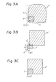
- Fig. 3A two rectangular image patterns P and P', which are projected by utilizing the rectangular electron beam 8 of Fig. 1, are illustrated.
- the pattern P is small in size, as is indicated by size information X 1 and Y 1
- the pattern P' is large in size, as is indicated by size information X 1 ' and Y 1 '.
- the peripheral sharpness of the large pattern P' is deteriorated as compared with that of the small pattern P.
- the origin O of the pattern P is substantially the same as the origin O' of the pattern P'. Note that the origins O and O' are determined by the periphery of the aperture 5 of the second mask 4.
- a refocusing operation according to the present invention is performed so as to improve the peripheral sharpness of the image patterns P and P'.
- the origin O' of the pattern P' is far away from the origin O of the pattern P since the axis of a refocusing coil for performing the above-mentioned refocusing operation does not alwasy coincide with the electron beam axis.
- the amount of shifting ⁇ X and the amount of shifting ⁇ Y of Fig. 3B are detected and, as a result, are in proportion to the area of the corresponding image pattern, such as P'.
- a flyback operation is performed so as to correct the shifting of position indicated by ⁇ X and ⁇ Y in F ig. 3B.
- a deflection unit for controlling the position of a projected beam is used.
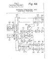
- Figure 4 which illustrates an embodiment of the present invention, is roughly divided into a beam-forming and beam--deffecting portion and a pattern-generating and pattern--control portion.
- Reference numeral 31 indicates an electron beam emitted. from an electron-gun 32, 33 indicates an anode, 34 indicates a cathode, 35 through 38 indicate aligning coils, 39 indicates a first mask, having a first rectangular aperture 39a, which corresponds to the mask 2 of Fig. 1, and 40 through 45 indicate de-magnifying lenses (coils).
- the last de-magnifying lens 45 is also called a projecting lens for projecting the electron beam 31 to a target plate 46, such as a wafer or a glass plate.
- Reference numerals 47X and 47Y indicate deflection units (plates) for determining the size of the electron beam 31 on the basis of the size information X l and Y l .
- the deflection units 47X and 47Y correspond to the deflection unit 7 of Fig. 1. Note that the deflection units 47X and 47Y are, of course, separated from each other; however, only one unit is illustrated so as to simplify the illustration.
- a second mask 48 having a second rectangular aperture 48a, which corresponds to the second «ask 4 of Fig. 1 is provided within the de-magnifying lens 42.
- the beam 31 shaped by the first aperture 39a, the second aperture 48a, and the deflection units 47X and 47Y passes through a pair of blanking plates 49, which plates determine whether the beam will be projected to the plate 46 or will be blanked.
- the beam 31 passes through the demagnifying lens 43, it passes through a round aperture 50a of a mask 50.
- the aperture 50a passes only the electrons passing through the center of the abovementioned optical system, including the de-magnifying lenses.
- the de-magnifying lens 44 images the rectangular beam 31 into the center of the projecting lens 45.
- an auxiliary converging coil, or a reforcusing coil 51 which is a coreless coil is provided so as to improve the peripheral sharpness of the beam 31.
- the lens 44 comprises coils 44a, an iron frame 44b enclosng the coils 44a, and ferrite pole pieces 44c.
- the ferrite pole pieces 44c prevent eddy currents and thereby enhance the response speed of the refocusing coil 51.
- deflection units 52X and 52Y are provided so as to deflect the beam 31 on the basis of the position information X 2 and Y 2 .
- the deflection units 52X and 52Y are electrostatic plates. Also, only one of the units 52X and 52Y is illustrated so as to implify the illustration.
- Reference numerals 53 and 54 indicate a dynamic focusing coil and a stigmatic coil, respectively, for dynamic correction, which is required when deflection of the beam is increased and the beam is far away from the optical axis.
- Reference numeral 61 designates a central processing unit (CPU) which controls the entire system; 62 designates a data memory for storing a plurality of rectangular exposure patterns, and 63 designates a pattern generator.
- the CPU 61, the data memory 62, and the pattern generator 63 are connected to each other with a data bus 64.
- the pattern generator 63 When a rectangular exposure pattern stored in the data memory is larger than a predetermined size, the rectangular exposure pattern is devided into a plurality of equal patterns by the pattern generator 63, which, in turn, generates equal patterns defined by the size information X 1 and Y 1 and the position information X 2 and Y 2 , shown in Fig. 6. In this case, X 1 ⁇ So and Y 1 ⁇ S 0 , wherein So is predetermined value.
- the pattern generator 63 will be explained in more detail.
- the size information X 1 is supplied through a digital--to- analog converter (DAC) 65 and an amplifier 66 to the deflection unit 47X while the size information Y 1 is supplied through a DAC 67 and an amplifier 68 to the deflection unit 47Y, with the result that the rectangular beam 31 is shaped or modified in accordance with the size information X 1 and Y 1 .
- a register 70 stores a compensation coefficient a, which is periodically renewed by the CPU 61.
- the values a and S are supplied to a multiplier 7, which calculates a value ⁇ S.
- the value ⁇ S is supplied through a DAC 72 and an amplifier 73 to the refocusing coil 51, with the result that the refocusing operation is performed in accordance with the magnitude of the cross section of the beam 31. That is, when the size S of the beam 31 is small, the refocusing coil 51 is controlled so as to weaken the converging effect thereof. Contrary to this, when the size S of the beam 31 is large, the refecusing coil 51 is controlled so as to strengthen the converging effect thereof. As a result, the beam 31 is converged at the same point of focus, regardless of the size S thereof.
- Registers 74 and 75 and multipliers 76 and 77 are used for the flyback operation, that is, correction of the axis of the beam 31. Also, the constants ⁇ X and ⁇ Y stored in the registers 74 and 75 are periodically renewed by the CPU 61.
- the amount of flyback ⁇ X and the amount of flyback ⁇ Y are calculated in accordance with the magnitude of the cross section S of the beam 31.
- the position information X 2 and Y 2 is processed by a correction circuit 78, which performs the following well--known correction calculations: where g X and g Y are gain coefficients, r X and r y are rotational coefficients, h x and h Y are trapezoidal coefficients, and O X and O Y are offset coefficients.
- the amount of flyback ⁇ X is added to the corrected position data X2 1 by an adder 79.
- the result X 2 1 + ⁇ X is supplied through a DAC 80 and an amplifier 81 to the deflection unit 52X.
- the amount of flyback ⁇ Y is added to the corrected position data Y 2 ' by an adder 82.
- the result Y 2 ' + ⁇ Y is supplied through a DAC converter 83 and an amplifier 8 to the deflection unit 52Y.
- deflection units exclusively for the flyback operation can also be provided. If such deflection units are provided, the values ⁇ X and ⁇ Y are supplied there to.
- Fig. 7 shows the distribution of the magnetic flux density in the path of the beam 31.
- the efficacy of the refocusing coil 51 is dependent on the magnetic field intensity or the magnetic flux density at the coil 51. That is, the focus distance f is represented by Therefore, the amount of shift of the focus ⁇ ( ) due to the refocusing coil 51 is represented by where ⁇ B is the change the magnetic flux density due to the refocusing coil 51.
- ⁇ B is the change the magnetic flux density due to the refocusing coil 51.
- the refocusing coil 51 is positioned within the de-magnifying lens 43. In this case, the refocusing coil 51 does not have a sufficient effect on the image projected onto the plate 46 since the distance between the refocusing coil 51 and the plate 46 is too great.
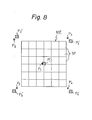
- MF indicates a main field determined by, for example, electromagnetic deflection means
- SF indicates a sub-field determined by, for example, electrostatic deflection means
- P 1 , P 2 , ... 1 P 5 indicate relatively small patterns
- P 1 ', P 2 ' , ..., P 5 ' indicate relatively large patterns.
- the small patterns F 1 , P 2 , ..., P 5 superpose the large patterns P 1 ', P 2 ', ..., P 5 ', respectively, before the refocusing operation.
- the refocusing coil 51 is positioned within the projecting lens 45, it is difficult to perform a flyback operation due to fluctuation of the relative shift in position between a small beam (pattern) and a large beam (pattern).
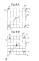
- the refocusing coil 51 When the refocusing coil 51 is positioned within the lens 44, as is illustrated in Fig. 4, the relative shift in position between a small beam and a large beam after the refocusing operation is uniform in each sub field, as is illustrated in Fig. 9A, since the aberration of the refocusing lens 51 is, in this case, small. Therefore, after the flyback operation is performed, the small patterns P 1 , P 2 ' ..., P 5 superpose the large patterns P 1 ', P 2 ', ..., P 5 ' , respectively, as is illustrated in 9B.
- the refocusing coil 51 be positioned within the lens 44, not within the lens 43 or 45.
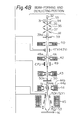
- the pattern generator 63 of Fig. 4 will now be explained in more detail with reference to Figs. 10, 11, and 12. If a rectangular exposure pattern stored in the data memory 62 of Fig. 4 is smaller than or equal to a predetermined size, the pattern generator 63 generates the same pattern as that stored in the data memory 62. Contrary to this, if a rectangular exposure pattern stored in the data memory 62 is larger than the above-mentioned predetermined size, the pattern generator 63 generates a plurality of patterns having the same size. That is, as is shown in Fig.
- the pattern generator 63 generates six patterns defined by the size information X 1 and Y 1 .
- the position information concerning the six patterns is defined by (X 20 , Y 20 ) , (X 20 + X 1 , Y 0 ) , ..., (X 20 + 2X 1 , Y 20 + Y 1 ) , respectively.
- the CPU 61 After the CPU 61 reads the information X 10 , Y 10 , X 20 , and Y 20 out of the data memory 62, the C PU 61 performs the operation illustrated in Fig- 12. Then the CPU 61 transmits the information X 1 and Y1 in addition to the information X 10 , Y 10 , X 20 , and Y 20 .
- step 1206 Contrary to this, if the answer at step 1202 is negative, the control proceeds to step 1205, in which X 1 ⁇ X 10 is performed.
- step 1206 the CPU 61 determines whether or not Y10 is larger than the value S 0 . If the answer at step 1206 is affirmative, the control proceeds to steps 1207 and 1208, in which the number N y of divided patterns and the size Y 1 of each divided pattern in the Y direction are calculated. Then the control proceeds to step 1210. Contrary to this, if the answer at step 1206 is negative, the control proceeds to step 1209 in which Y 1 ⁇ Y10 is preformed. Next, the control proceeds to step 1210, in which the operation of Fig. 12 is completed.
- reference numerals 1001 through 1006 designate registers for receiving the information X 1 X 10 , Y 1 , Y 10 , X 20 , and Y 20 , resp ec- tively, from the CPU 61; 1007 and 1008 designate registers for storing the remainder of divided patterns in the X direction and the Y direction, respectively; 1009 and 1010 designate registers for storing the position information X 2 and Y 2 of each divided pattern; 1011 and 1012 designate subtracters; 1013 and 1014 designate adders; 1015 and 1016 designate comparators; 1017 and 1018 designate AND circuits. It is assumed that small values such as X 1 /2 and Y 1 /2 are applied by the CPU 61 to the (+) inputs of the comparator 1015 and the comparator 1016, respectively.
- the value of the register 1007 is X 10 (> X 1 /2), the output of the comparator 1015 remains low, the value of the register 1 00 8 is Y 20 (> Y 1 /2), and the output of the comparator 1016 remains low.
- a clock signal CK2 from the CPU 61 is generated to operate the adder 1013.
- the value of the register 1019 is changed from X 20 to X 20 + X 1 . Therefore, the position parameters of the second patter P 2 are
- the subtracter 1011 is operated so that the value of the register 1007 is changed from X 10 to X 10 - X 1 ( ⁇ 2X 1 ). Therefore, the output of the comparator 1015 does not change.
- a clock signal CK2 from the CPU 61 is generated to operate the adder 1013.
- the value of the register 1019 is changed from X 20 + X 1 to X 20 + 2X 1 . Therefore, the position parameters of the third pattern P 3 are
- the subtracter 1011 is operated so that the value of the register 1007 is changed from X 10 - X 1 to X 10 2X 1 ( ⁇ X 1 ). Therefore, the output of the comparator 1015 does not change.
- a clock signal CK2 from the CPU 61 is generated to operate the adder 1013.
- the value of the register 1009 is changed from X 20 + 2X 1 to X 20 + 3X 1 .
- the subtracter 1011 is operated so that the value of the register 1007 is changed from X 10 - 2X 1 to X 10 - 3X 1 ( ⁇ 0), and, accordingly, the output of the comparator 1015 is changed from low to high.
- the values X 10 and X 20 are again set in the registers 1007 and 1009, respectively.
- the subtracter 1012 is operated so that the value of the register 1008 is changed from Y 10 to Y 10 - Y 1 ( ⁇ Y 1 )
- the adder 1014 is operated so that the value of the register 1010 is changed from Y 20 to Y 20 + Y 1 . Therefore, the position parameters of the fourth pattern P 4 are
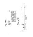
- Fig. 13A patterns 131 and 132 are smaller than the predetermined size, and a pattern 13 is larger than the predetermined size so that the pattern 13 is divided into a plurality of identical patterns 133 through 150.
- the current If flowing through the refocusing coil 51 changes, as is shown in Fig. 13B.
- the number of current transitions- is small, and, accordingly, the entire exposure time is small.
- the shaded portions indicate transitions of the current I f , in which the beam 31 is blanked to stop the exposure operation.
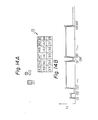
- the pattern 13 is divided into a plurality of patterns 133' through 150'.
- the patterns 133' through 137' and the patterns 139' through 143' have the same size (SO x SO), the other patterns 138' and 144' through 150' being smaller than the predetermined size. Therefore, when the exposure operation is performed the patterns 131, 132, and 133' through 150', in that order, the current If flowing through the refocusing coil 51 changes, as is shown in Fig. 14B. As a result, the number of current transtions is large, and, accordingly, the entire exposure time is increased as compared with the case illustrated in Figs. 13A and 13B.
- the peripheral sharpness of a projected image is improved by a refocusing operation in accordance with the magnitude of the cross-section of a beam.
Landscapes
- Chemical & Material Sciences (AREA)
- Analytical Chemistry (AREA)
- Electron Beam Exposure (AREA)
Applications Claiming Priority (2)
| Application Number | Priority Date | Filing Date | Title |
|---|---|---|---|
| JP211201/81 | 1981-12-28 | ||
| JP56211201A JPS58121625A (ja) | 1981-12-28 | 1981-12-28 | 電子ビ−ム露光装置 |
Publications (3)
| Publication Number | Publication Date |
|---|---|
| EP0083246A2 true EP0083246A2 (de) | 1983-07-06 |
| EP0083246A3 EP0083246A3 (en) | 1986-05-14 |
| EP0083246B1 EP0083246B1 (de) | 1989-08-02 |
Family
ID=16602033
Family Applications (1)
| Application Number | Title | Priority Date | Filing Date |
|---|---|---|---|
| EP82306994A Expired EP0083246B1 (de) | 1981-12-28 | 1982-12-30 | Rasterelektronenstrahl-Belichtungssystem |
Country Status (4)
| Country | Link |
|---|---|
| US (1) | US4968893A (de) |
| EP (1) | EP0083246B1 (de) |
| JP (1) | JPS58121625A (de) |
| DE (1) | DE3279856D1 (de) |
Cited By (3)
| Publication number | Priority date | Publication date | Assignee | Title |
|---|---|---|---|---|
| US4647782A (en) * | 1982-09-30 | 1987-03-03 | Tokyo Shibaura Denki Kabushiki Kaisha | Charged particle beam exposure apparatus |
| EP0421695A3 (en) * | 1989-09-30 | 1991-09-04 | Fujitsu Limited | Electron beam exposuring device and exposuring method using the same |
| EP0434990A3 (en) * | 1989-11-30 | 1991-09-11 | Fujitsu Limited | Charged-particle beam exposure method and apparatus |
Families Citing this family (5)
| Publication number | Priority date | Publication date | Assignee | Title |
|---|---|---|---|---|
| JPS5932128A (ja) * | 1982-08-18 | 1984-02-21 | Nippon Telegr & Teleph Corp <Ntt> | 荷電ビ−ム露光装置におけるビ−ム照射位置補正方法 |
| JP2651298B2 (ja) * | 1991-10-29 | 1997-09-10 | 富士通株式会社 | ビーム焦点調整器及び電子ビーム装置 |
| US7394080B2 (en) * | 2004-12-23 | 2008-07-01 | Taiwan Semiconductor Manufacturing Company, Ltd. | Mask superposition for multiple exposures |
| DE102007046783A1 (de) * | 2007-09-29 | 2009-04-23 | Carl Zeiss Nts Gmbh | Vorrichtung zur Ablenkung oder Einlenkung eines Teilchenstrahls |
| JP5528753B2 (ja) * | 2009-09-25 | 2014-06-25 | 株式会社アドバンテスト | 電子ビーム露光装置 |
Family Cites Families (6)
| Publication number | Priority date | Publication date | Assignee | Title |
|---|---|---|---|---|
| JPS5283177A (en) * | 1975-12-31 | 1977-07-11 | Fujitsu Ltd | Electron beam exposure device |
| JPS54374A (en) * | 1977-05-30 | 1979-01-05 | Nippon Yusoki Co Ltd | Controller of unmanned travelling car |
| JPS5493364A (en) * | 1977-12-30 | 1979-07-24 | Fujitsu Ltd | Exposure system for electron beam |
| JPS5693318A (en) * | 1979-12-10 | 1981-07-28 | Fujitsu Ltd | Electron beam exposure device |
| JPS5694740A (en) * | 1979-12-28 | 1981-07-31 | Fujitsu Ltd | Electronic beam exposure device |
| JPS56147437A (en) * | 1980-04-17 | 1981-11-16 | Fujitsu Ltd | Electron beam exposure method |
-
1981
- 1981-12-28 JP JP56211201A patent/JPS58121625A/ja active Granted
-
1982
- 1982-12-30 EP EP82306994A patent/EP0083246B1/de not_active Expired
- 1982-12-30 DE DE8282306994T patent/DE3279856D1/de not_active Expired
-
1989
- 1989-04-18 US US07/339,887 patent/US4968893A/en not_active Expired - Lifetime
Cited By (4)
| Publication number | Priority date | Publication date | Assignee | Title |
|---|---|---|---|---|
| US4647782A (en) * | 1982-09-30 | 1987-03-03 | Tokyo Shibaura Denki Kabushiki Kaisha | Charged particle beam exposure apparatus |
| EP0421695A3 (en) * | 1989-09-30 | 1991-09-04 | Fujitsu Limited | Electron beam exposuring device and exposuring method using the same |
| EP0434990A3 (en) * | 1989-11-30 | 1991-09-11 | Fujitsu Limited | Charged-particle beam exposure method and apparatus |
| US5130547A (en) * | 1989-11-30 | 1992-07-14 | Fujitsu Limited | Charged-particle beam exposure method and apparatus |
Also Published As
| Publication number | Publication date |
|---|---|
| JPS58121625A (ja) | 1983-07-20 |
| DE3279856D1 (en) | 1989-09-07 |
| EP0083246A3 (en) | 1986-05-14 |
| JPH047088B2 (de) | 1992-02-07 |
| US4968893A (en) | 1990-11-06 |
| EP0083246B1 (de) | 1989-08-02 |
Similar Documents
| Publication | Publication Date | Title |
|---|---|---|
| US6107636A (en) | Electron beam exposure apparatus and its control method | |
| US6137113A (en) | Electron beam exposure method and apparatus | |
| JP4756776B2 (ja) | 荷電粒子線露光装置、荷電粒子線露光方法およびデバイス製造方法 | |
| KR100537127B1 (ko) | 에너지 빔 노광 방법 및 노광 장치 | |
| US6552353B1 (en) | Multi-electron beam exposure method and apparatus and device manufacturing method | |
| US20080179536A1 (en) | Changed particle beam emitting device and method for adjusting the optical axis | |
| EP0419287B1 (de) | Verfahren zur Korrektur des Astigmatismus eines Strahles dessen Querschnittsform veränderbar ist | |
| EP0580212A1 (de) | Stigmator mit variabler Achse | |
| JP2006100336A (ja) | 電子ビーム露光用マスク、電子ビーム露光方法及び電子ビーム露光装置 | |
| US6657210B1 (en) | Electron beam exposure method, a method of constructing exposure control data, and a computer-readable medium | |
| US7041988B2 (en) | Electron beam exposure apparatus and electron beam processing apparatus | |
| EP0083246A2 (de) | Rasterelektronenstrahl-Belichtungssystem | |
| US7388214B2 (en) | Charged-particle beam exposure apparatus and method | |
| JP2002299207A (ja) | 荷電粒子ビーム描画装置 | |
| JP6823823B2 (ja) | 荷電粒子ビーム描画装置、その制御方法および補正描画データ作成方法 | |
| US6066853A (en) | Electron-optical system exhibiting reduced aberration | |
| EP0182360B1 (de) | System zum kontinuierlichen Belichten gewünschter Muster und deren Hintergründe auf einer Target-Oberfläche | |
| US4710640A (en) | Electron beam lithography | |
| JPWO2008044479A1 (ja) | 電子ビーム露光装置及び電子ビーム露光方法 | |
| US6049084A (en) | Charged-particle-beam optical system | |
| JP2006294962A (ja) | 電子ビーム描画装置および描画方法 | |
| JP3976835B2 (ja) | 電子ビーム露光方法及び電子ビーム露光装置 | |
| JP2001118765A (ja) | 荷電粒子線露光装置、荷電粒子線露光装置の調整方法及び半導体デバイスの製造方法 | |
| JPH1064794A (ja) | 電子ビーム露光補正方法 | |
| JP2003332206A (ja) | 電子ビーム露光装置及び電子ビーム処理装置 |
Legal Events
| Date | Code | Title | Description |
|---|---|---|---|
| PUAI | Public reference made under article 153(3) epc to a published international application that has entered the european phase |
Free format text: ORIGINAL CODE: 0009012 |
|
| AK | Designated contracting states |
Designated state(s): DE FR GB |
|
| PUAL | Search report despatched |
Free format text: ORIGINAL CODE: 0009013 |
|
| AK | Designated contracting states |
Kind code of ref document: A3 Designated state(s): DE FR GB |
|
| 17P | Request for examination filed |
Effective date: 19860912 |
|
| 17Q | First examination report despatched |
Effective date: 19880219 |
|
| GRAA | (expected) grant |
Free format text: ORIGINAL CODE: 0009210 |
|
| AK | Designated contracting states |
Kind code of ref document: B1 Designated state(s): DE FR GB |
|
| REF | Corresponds to: |
Ref document number: 3279856 Country of ref document: DE Date of ref document: 19890907 |
|
| ET | Fr: translation filed | ||
| PLBE | No opposition filed within time limit |
Free format text: ORIGINAL CODE: 0009261 |
|
| STAA | Information on the status of an ep patent application or granted ep patent |
Free format text: STATUS: NO OPPOSITION FILED WITHIN TIME LIMIT |
|
| 26N | No opposition filed | ||
| PGFP | Annual fee paid to national office [announced via postgrant information from national office to epo] |
Ref country code: GB Payment date: 19981231 Year of fee payment: 17 |
|
| PGFP | Annual fee paid to national office [announced via postgrant information from national office to epo] |
Ref country code: FR Payment date: 19991208 Year of fee payment: 18 |
|
| PG25 | Lapsed in a contracting state [announced via postgrant information from national office to epo] |
Ref country code: GB Free format text: LAPSE BECAUSE OF NON-PAYMENT OF DUE FEES Effective date: 19991230 |
|
| PGFP | Annual fee paid to national office [announced via postgrant information from national office to epo] |
Ref country code: DE Payment date: 19991231 Year of fee payment: 18 |
|
| GBPC | Gb: european patent ceased through non-payment of renewal fee |
Effective date: 19991230 |
|
| PG25 | Lapsed in a contracting state [announced via postgrant information from national office to epo] |
Ref country code: FR Free format text: LAPSE BECAUSE OF NON-PAYMENT OF DUE FEES Effective date: 20010831 |
|
| REG | Reference to a national code |
Ref country code: FR Ref legal event code: ST |
|
| PG25 | Lapsed in a contracting state [announced via postgrant information from national office to epo] |
Ref country code: DE Free format text: LAPSE BECAUSE OF NON-PAYMENT OF DUE FEES Effective date: 20011002 |