EP0083265A1 - Support d'interconnexion d'un boîtier de circuit intégré sur un circuit imprimé, et système d'interconnexion utilisant un tel support - Google Patents
Support d'interconnexion d'un boîtier de circuit intégré sur un circuit imprimé, et système d'interconnexion utilisant un tel support Download PDFInfo
- Publication number
- EP0083265A1 EP0083265A1 EP82402290A EP82402290A EP0083265A1 EP 0083265 A1 EP0083265 A1 EP 0083265A1 EP 82402290 A EP82402290 A EP 82402290A EP 82402290 A EP82402290 A EP 82402290A EP 0083265 A1 EP0083265 A1 EP 0083265A1
- Authority
- EP
- European Patent Office
- Prior art keywords
- interconnection
- support
- printed circuit
- contacts
- series
- Prior art date
- Legal status (The legal status is an assumption and is not a legal conclusion. Google has not performed a legal analysis and makes no representation as to the accuracy of the status listed.)
- Granted
Links
Images

Classifications
-
- H—ELECTRICITY
- H10—SEMICONDUCTOR DEVICES; ELECTRIC SOLID-STATE DEVICES NOT OTHERWISE PROVIDED FOR
- H10W—GENERIC PACKAGES, INTERCONNECTIONS, CONNECTORS OR OTHER CONSTRUCTIONAL DETAILS OF DEVICES COVERED BY CLASS H10
- H10W70/00—Package substrates; Interposers; Redistribution layers [RDL]
- H10W70/60—Insulating or insulated package substrates; Interposers; Redistribution layers
- H10W70/611—Insulating or insulated package substrates; Interposers; Redistribution layers for connecting multiple chips together
-
- H—ELECTRICITY
- H05—ELECTRIC TECHNIQUES NOT OTHERWISE PROVIDED FOR
- H05K—PRINTED CIRCUITS; CASINGS OR CONSTRUCTIONAL DETAILS OF ELECTRIC APPARATUS; MANUFACTURE OF ASSEMBLAGES OF ELECTRICAL COMPONENTS
- H05K1/00—Printed circuits
- H05K1/02—Details
- H05K1/0271—Arrangements for reducing stress or warp in rigid printed circuit boards, e.g. caused by loads, vibrations or differences in thermal expansion
-
- H—ELECTRICITY
- H05—ELECTRIC TECHNIQUES NOT OTHERWISE PROVIDED FOR
- H05K—PRINTED CIRCUITS; CASINGS OR CONSTRUCTIONAL DETAILS OF ELECTRIC APPARATUS; MANUFACTURE OF ASSEMBLAGES OF ELECTRICAL COMPONENTS
- H05K1/00—Printed circuits
- H05K1/02—Details
- H05K1/14—Structural association of two or more printed circuits
- H05K1/141—One or more single auxiliary printed circuits mounted on a main printed circuit, e.g. modules, adapters
-
- H—ELECTRICITY
- H05—ELECTRIC TECHNIQUES NOT OTHERWISE PROVIDED FOR
- H05K—PRINTED CIRCUITS; CASINGS OR CONSTRUCTIONAL DETAILS OF ELECTRIC APPARATUS; MANUFACTURE OF ASSEMBLAGES OF ELECTRICAL COMPONENTS
- H05K1/00—Printed circuits
- H05K1/18—Printed circuits structurally associated with non-printed electric components
- H05K1/189—Printed circuits structurally associated with non-printed electric components characterised by the use of flexible or folded printed circuits
-
- H—ELECTRICITY
- H05—ELECTRIC TECHNIQUES NOT OTHERWISE PROVIDED FOR
- H05K—PRINTED CIRCUITS; CASINGS OR CONSTRUCTIONAL DETAILS OF ELECTRIC APPARATUS; MANUFACTURE OF ASSEMBLAGES OF ELECTRICAL COMPONENTS
- H05K3/00—Apparatus or processes for manufacturing printed circuits
- H05K3/30—Assembling printed circuits with electric components, e.g. with resistors
- H05K3/32—Assembling printed circuits with electric components, e.g. with resistors electrically connecting electric components or wires to printed circuits
- H05K3/34—Assembling printed circuits with electric components, e.g. with resistors electrically connecting electric components or wires to printed circuits by soldering
- H05K3/341—Surface mounted components
- H05K3/3431—Leadless components
- H05K3/3442—Leadless components having edge contacts, e.g. leadless chip capacitors, chip carriers
-
- H—ELECTRICITY
- H10—SEMICONDUCTOR DEVICES; ELECTRIC SOLID-STATE DEVICES NOT OTHERWISE PROVIDED FOR
- H10W—GENERIC PACKAGES, INTERCONNECTIONS, CONNECTORS OR OTHER CONSTRUCTIONAL DETAILS OF DEVICES COVERED BY CLASS H10
- H10W70/00—Package substrates; Interposers; Redistribution layers [RDL]
- H10W70/60—Insulating or insulated package substrates; Interposers; Redistribution layers
- H10W70/67—Insulating or insulated package substrates; Interposers; Redistribution layers characterised by their insulating layers or insulating parts
- H10W70/68—Shapes or dispositions thereof
- H10W70/685—Shapes or dispositions thereof comprising multiple insulating layers
-
- H—ELECTRICITY
- H10—SEMICONDUCTOR DEVICES; ELECTRIC SOLID-STATE DEVICES NOT OTHERWISE PROVIDED FOR
- H10W—GENERIC PACKAGES, INTERCONNECTIONS, CONNECTORS OR OTHER CONSTRUCTIONAL DETAILS OF DEVICES COVERED BY CLASS H10
- H10W70/00—Package substrates; Interposers; Redistribution layers [RDL]
- H10W70/60—Insulating or insulated package substrates; Interposers; Redistribution layers
- H10W70/67—Insulating or insulated package substrates; Interposers; Redistribution layers characterised by their insulating layers or insulating parts
- H10W70/688—Flexible insulating substrates
-
- H—ELECTRICITY
- H10—SEMICONDUCTOR DEVICES; ELECTRIC SOLID-STATE DEVICES NOT OTHERWISE PROVIDED FOR
- H10W—GENERIC PACKAGES, INTERCONNECTIONS, CONNECTORS OR OTHER CONSTRUCTIONAL DETAILS OF DEVICES COVERED BY CLASS H10
- H10W90/00—Package configurations
- H10W90/401—Package configurations characterised by multiple insulating or insulated package substrates, interposers or RDLs
-
- H—ELECTRICITY
- H05—ELECTRIC TECHNIQUES NOT OTHERWISE PROVIDED FOR
- H05K—PRINTED CIRCUITS; CASINGS OR CONSTRUCTIONAL DETAILS OF ELECTRIC APPARATUS; MANUFACTURE OF ASSEMBLAGES OF ELECTRICAL COMPONENTS
- H05K2201/00—Indexing scheme relating to printed circuits covered by H05K1/00
- H05K2201/04—Assemblies of printed circuits
- H05K2201/049—PCB for one component, e.g. for mounting onto mother PCB
-
- H—ELECTRICITY
- H05—ELECTRIC TECHNIQUES NOT OTHERWISE PROVIDED FOR
- H05K—PRINTED CIRCUITS; CASINGS OR CONSTRUCTIONAL DETAILS OF ELECTRIC APPARATUS; MANUFACTURE OF ASSEMBLAGES OF ELECTRICAL COMPONENTS
- H05K2201/00—Indexing scheme relating to printed circuits covered by H05K1/00
- H05K2201/09—Shape and layout
- H05K2201/09009—Substrate related
- H05K2201/09063—Holes or slots in insulating substrate not used for electrical connections
-
- H—ELECTRICITY
- H05—ELECTRIC TECHNIQUES NOT OTHERWISE PROVIDED FOR
- H05K—PRINTED CIRCUITS; CASINGS OR CONSTRUCTIONAL DETAILS OF ELECTRIC APPARATUS; MANUFACTURE OF ASSEMBLAGES OF ELECTRICAL COMPONENTS
- H05K2201/00—Indexing scheme relating to printed circuits covered by H05K1/00
- H05K2201/09—Shape and layout
- H05K2201/09009—Substrate related
- H05K2201/09072—Hole or recess under component or special relationship between hole and component
-
- H—ELECTRICITY
- H05—ELECTRIC TECHNIQUES NOT OTHERWISE PROVIDED FOR
- H05K—PRINTED CIRCUITS; CASINGS OR CONSTRUCTIONAL DETAILS OF ELECTRIC APPARATUS; MANUFACTURE OF ASSEMBLAGES OF ELECTRICAL COMPONENTS
- H05K2201/00—Indexing scheme relating to printed circuits covered by H05K1/00
- H05K2201/09—Shape and layout
- H05K2201/09009—Substrate related
- H05K2201/09081—Tongue or tail integrated in planar structure, e.g. obtained by cutting from the planar structure
-
- H—ELECTRICITY
- H05—ELECTRIC TECHNIQUES NOT OTHERWISE PROVIDED FOR
- H05K—PRINTED CIRCUITS; CASINGS OR CONSTRUCTIONAL DETAILS OF ELECTRIC APPARATUS; MANUFACTURE OF ASSEMBLAGES OF ELECTRICAL COMPONENTS
- H05K2201/00—Indexing scheme relating to printed circuits covered by H05K1/00
- H05K2201/09—Shape and layout
- H05K2201/09145—Edge details
- H05K2201/09172—Notches between edge pads
-
- H—ELECTRICITY
- H05—ELECTRIC TECHNIQUES NOT OTHERWISE PROVIDED FOR
- H05K—PRINTED CIRCUITS; CASINGS OR CONSTRUCTIONAL DETAILS OF ELECTRIC APPARATUS; MANUFACTURE OF ASSEMBLAGES OF ELECTRICAL COMPONENTS
- H05K2201/00—Indexing scheme relating to printed circuits covered by H05K1/00
- H05K2201/10—Details of components or other objects attached to or integrated in a printed circuit board
- H05K2201/10613—Details of electrical connections of non-printed components, e.g. special leads
- H05K2201/10621—Components characterised by their electrical contacts
- H05K2201/10666—Plated through-hole for surface mounting on PCB
-
- H—ELECTRICITY
- H05—ELECTRIC TECHNIQUES NOT OTHERWISE PROVIDED FOR
- H05K—PRINTED CIRCUITS; CASINGS OR CONSTRUCTIONAL DETAILS OF ELECTRIC APPARATUS; MANUFACTURE OF ASSEMBLAGES OF ELECTRICAL COMPONENTS
- H05K2201/00—Indexing scheme relating to printed circuits covered by H05K1/00
- H05K2201/10—Details of components or other objects attached to or integrated in a printed circuit board
- H05K2201/10613—Details of electrical connections of non-printed components, e.g. special leads
- H05K2201/10621—Components characterised by their electrical contacts
- H05K2201/10727—Leadless chip carrier [LCC], e.g. chip-modules for cards
-
- H—ELECTRICITY
- H05—ELECTRIC TECHNIQUES NOT OTHERWISE PROVIDED FOR
- H05K—PRINTED CIRCUITS; CASINGS OR CONSTRUCTIONAL DETAILS OF ELECTRIC APPARATUS; MANUFACTURE OF ASSEMBLAGES OF ELECTRICAL COMPONENTS
- H05K2201/00—Indexing scheme relating to printed circuits covered by H05K1/00
- H05K2201/20—Details of printed circuits not provided for in H05K2201/01 - H05K2201/10
- H05K2201/2036—Permanent spacer or stand-off in a printed circuit or printed circuit assembly
-
- H—ELECTRICITY
- H05—ELECTRIC TECHNIQUES NOT OTHERWISE PROVIDED FOR
- H05K—PRINTED CIRCUITS; CASINGS OR CONSTRUCTIONAL DETAILS OF ELECTRIC APPARATUS; MANUFACTURE OF ASSEMBLAGES OF ELECTRICAL COMPONENTS
- H05K3/00—Apparatus or processes for manufacturing printed circuits
- H05K3/30—Assembling printed circuits with electric components, e.g. with resistors
- H05K3/303—Assembling printed circuits with electric components, e.g. with resistors with surface mounted components
-
- H—ELECTRICITY
- H05—ELECTRIC TECHNIQUES NOT OTHERWISE PROVIDED FOR
- H05K—PRINTED CIRCUITS; CASINGS OR CONSTRUCTIONAL DETAILS OF ELECTRIC APPARATUS; MANUFACTURE OF ASSEMBLAGES OF ELECTRICAL COMPONENTS
- H05K3/00—Apparatus or processes for manufacturing printed circuits
- H05K3/36—Assembling printed circuits with other printed circuits
- H05K3/368—Assembling printed circuits with other printed circuits parallel to each other
-
- H—ELECTRICITY
- H10—SEMICONDUCTOR DEVICES; ELECTRIC SOLID-STATE DEVICES NOT OTHERWISE PROVIDED FOR
- H10W—GENERIC PACKAGES, INTERCONNECTIONS, CONNECTORS OR OTHER CONSTRUCTIONAL DETAILS OF DEVICES COVERED BY CLASS H10
- H10W72/00—Interconnections or connectors in packages
- H10W72/071—Connecting or disconnecting
- H10W72/072—Connecting or disconnecting of bump connectors
- H10W72/07251—Connecting or disconnecting of bump connectors characterised by changes in properties of the bump connectors during connecting
-
- H—ELECTRICITY
- H10—SEMICONDUCTOR DEVICES; ELECTRIC SOLID-STATE DEVICES NOT OTHERWISE PROVIDED FOR
- H10W—GENERIC PACKAGES, INTERCONNECTIONS, CONNECTORS OR OTHER CONSTRUCTIONAL DETAILS OF DEVICES COVERED BY CLASS H10
- H10W72/00—Interconnections or connectors in packages
- H10W72/20—Bump connectors, e.g. solder bumps or copper pillars; Dummy bumps; Thermal bumps
-
- Y—GENERAL TAGGING OF NEW TECHNOLOGICAL DEVELOPMENTS; GENERAL TAGGING OF CROSS-SECTIONAL TECHNOLOGIES SPANNING OVER SEVERAL SECTIONS OF THE IPC; TECHNICAL SUBJECTS COVERED BY FORMER USPC CROSS-REFERENCE ART COLLECTIONS [XRACs] AND DIGESTS
- Y02—TECHNOLOGIES OR APPLICATIONS FOR MITIGATION OR ADAPTATION AGAINST CLIMATE CHANGE
- Y02P—CLIMATE CHANGE MITIGATION TECHNOLOGIES IN THE PRODUCTION OR PROCESSING OF GOODS
- Y02P70/00—Climate change mitigation technologies in the production process for final industrial or consumer products
- Y02P70/50—Manufacturing or production processes characterised by the final manufactured product
Definitions
- the present invention relates to the interconnection of integrated circuit packages of the type known by the Anglo-Saxon name "chip-carrier" on a printed circuit.
- chips constituting large-scale integrated circuits are generally placed in boxes comprising a ceramic base coated with screen-printed electrical contacts to which the chip output contacts are generally connected by thermo-compression.
- integrated circuit boxes are generally called in English terminology "chip-carrier", a term which will be used throughout the remainder of this description.
- the ceramic constituting these chip carriers has a very low coefficient of thermal expansion and more generally a very good temperature resistance which justifies its use in this type of application.
- These chip carriers are intended for implantation on multi-layer printed circuit boards which are themselves part of electronic devices.
- the interconnection between the chip-carrier and the printed circuit is done either by means of connectors, or by means of particularly adapted bases.
- These "chip-carriers" cannot be soldered directly on the printed circuits because they have a coefficient of thermal expansion significantly higher than that of ceramic, which causes during thermal cycles undergone by the printed card, a tearing at the interconnection contacts of the chip-carrier and the printed circuit.
- the interconnection support according to the invention makes it possible to simply solve the problem posed.
- it is characterized in that it is constituted by a flexible dielectric having the shape of a crown pierced with a central opening and provided on one of its faces with a first series of electrical contacts, each contact extending substantially to the edge of the central opening, and on the other of its faces with a second series of contacts, each of them being connected to one of the contacts of the first series, and arranged substantially at the periphery of the crown so as to leave a free surface between each contact of the second series and the edge of the opening.
- this interconnection support will preferably include a plurality of slots extending from the central opening substantially to the second series of contacts.
- the invention also relates to a system for interconnecting a chip carrier on a printed circuit using a support as described above.
- This system is characterized in that said support is interposed between the housing and the printed circuit, each contact of the first series being connected to one of the contacts of the chip carrier, while each contact of the second series is connected to one of the contacts of the printed circuit, the distance, in a section perpendicular to the whole system, between the edges of the opening (d l ) being less than that between the opposite contacts of the second series (d 4 ) so as to leave a free space of width (d 5) between the flexible dielectric (7) and the printed circuit (38) thus making it possible to absorb without damaging the contacts (2, 33, 35, 44) the different thermal expansions of the housing (36) and of the printed circuit (38).
- Such an interconnection system makes it possible in particular to considerably increase the density of the chip carriers on the printed circuit.
- the printed circuit is a quite usual circuit, and can have metallized interconnection holes between the different layers placed under the chip-carrier. In this way, it is thus possible to place several chip-carriers side by side without being obliged to separate them by rows of metallized interconnection holes.
- the interconnection system according to the invention is also remarkable in that the interconnection support comprises positioning means which cooperate with complementary positioning means arranged on the circuit, allowing simultaneous soldering of the housing on the support. and support on the circuit.
- FIG. 1 shows an interconnection support (1) according to the invention.
- This interconnection support here has the shape of a square with sides 50, 51, 52 and 53. It consists of a flexible dielectric 7 which has a central opening 20 which itself has the shape of a square of sides 21 , 22, 23 and 24. Slots 8, 9, 10 and 11 arranged substantially along the diagonals of this square extend from the central opening 20 to near the end of the electrical contacts 2. These slots terminate respectively in circular parts 12, 13, 14 and 15 preventing the support 1 from tearing in the event of deformation.
- the support 1 is coated on its upper face shown in FIG. 1 with a plurality of electrical contacts 2, these contacts being in the case of this figure 16 in number, that is to say four contacts along each edge of the opening 20.
- These electrical contacts 2 comprise a part 6 disposed near the corresponding edge of the opening 20, extended by a part of narrower width 5, ending in a wider part 3, substantially similarly width as that of part 6.
- This part 3 is arranged not far from the corresponding edge 51 of the support 1. It comprises a part 4 representing a metallized hole for the interconnection of this electrical contact 2 with a corresponding electrical contact 33 (FIG. 2 ).
- a part 4 representing a metallized hole for the interconnection of this electrical contact 2 with a corresponding electrical contact 33 (FIG. 2 ).
- four centering holes 16, 17, 18, 19 are arranged making it possible to correctly position the support on the printed circuit before the soldering operation.
- Also shown in dotted lines in this figure is the outer contour of the chip carrier, materialized by its sides 25, 26, 27 and 28.
- the width of the square opening 20 is equal to d i , the distance between two contacts 2 in vis-à-vis each other is equal to d 21 the external dimension of the chip-carrier is equal to d 3 , while the distance between the rear parts 3 of the contacts 2, between two contacts facing -vis, is equal to d . .
- the distance between the edge of the opening 20 and the end of a row of end contacts 3 is equal to d5.
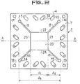
- FIG. 2 the back of the support illustrated in FIG. 1 is shown, the same elements bearing the same references.
- a plurality of contacts 33 forming a second series of electrical contacts is disposed substantially at the periphery of the support 1.
- Each of these contacts 33 is connected via the metallized hole 4 to one of the contacts 2 on the upper face.
- the set of metallized holes 4 is substantially aligned with the positioning holes such as 16 and 17 arranged on the edges of the support 1.
- the back of the support 1 therefore has a part of width d5 between the end of the contacts such as 33 and the corresponding edge of the opening 20 is an area without electrical contact in which the dielectric of the support is exposed.
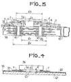
- FIG 3 provides a better understanding of the use of the interconnection support according to the invention as shown in Figures 1 and 2.
- This Figure 3 shows a sectional view of a chip-carrier 36 interconnected using the support 1 to a multi-layer printed circuit 38, this sectional view being taken along the axis AA of the previous figures.
- the external contacts 35, for example screen-printed, of the chip-carrier 36 are connected via the solder pads 34 to the electrical contacts 2. These are connected via the metallized hole 4 to the electrical contacts 33 located on the back of the dielectric support 7.
- These metallized contacts 33 are themselves reflected by means of solder pads with electrical contacts such as 39 and 44 of the multi-layer printed circuit 38.
- the latter has a plurality of conductive layers, represented by hatched lines in the figure, separated by insulating dielectric layers, said conductive layers being interconnected by means of metallized holes such as 41, 43 and 45.
- the interconnection of the chip-carrier 36 on the multi-circuit board layers 38 being effected after the production of said multi-layer printed circuit 38, it can therefore include metallized interconnection holes such as 41 and 43 located under said chip-carri er 36, that is to say inside the surface delimited by the electrical contacts such as 33.
- the interconnection support 1 is positioned on the multi-layer printed circuit 38, for example by threading the interconnection support 1 on lugs (at least two) previously positioned on the printed circuit 38, using positioning holes 16, 17, 18, 19 which allow the contacts 33 to be placed exactly above the corresponding contacts of the printed circuit 38.
- the relative positioning of the interconnection support and of the printed circuit can also be achieved by carrying out protuberances or deformations, of any shape in the interconnection support itself. hot deformation of the interconnection support or a hole with deformation on one side of the hole).
- the chip-carrier 36 is placed on top of the interconnection support 1.
- All of the electrical contacts are then soldered, for example in the vapor phase, bringing the temperature of the entire system to the melting temperature of the solder previously placed in the appropriate places (34 and 37). It is a particularly important advantage of the invention to allow the same type of solder to be used at locations 34 and 37, since the soldering of the chip carrier on the interconnection support 1 and the soldering of the latter on the printed circuit 38 can be produced simultaneously, therefore at the same temperature.
- a support 1 is made of polyimide film 50 microns thick covered with electrical contacts 2 made of copper, in which a central opening 20 with a width of 4.5 mm had been made.
- the external dimensions of the support 1 were those of a square with a side of 14.5 mm.
- the diagonal slots such as 8 had a length of the order of 4 mm and ended in a circular part of 0.8 mm in diameter.
- the distance d 4 between the contacts 33 of the lower face was of the order of 11 mm, thus leaving a distance d5 free of electrical contacts with a width of the order of 3 mm.
- an interconnection support according to the invention After having simultaneously brazed in vapor phase a chip carrier, an interconnection support according to the invention and a printed circuit board, the assembly was subjected to 500 thermal cycles. During each of them, the whole is heated for 30 min at -55 ° C and then for 30 min at + 125 ° C. The passage from - 55 ° C to + 125 ° C and vice-versa (transfer from one oven to another) must be done in less than 2 minutes. After 500 cycles, no degradation of the various interconnections was observed.
- the circuit board 38 used here consists of a heat sink 61 coated with a thin printed circuit 60 in which an opening 63 has been made under the "chip-carrier" 36.
- This opening 63 has a width less than or equal to the width d of the interconnection support 1.
- a thermally conductive paste 62 is introduced into this opening 63 as far as the chip carrier 36, on a thickness e.
- This paste can for example be a paste of polymerized silicones, loaded with thermally conductive particles.
- This thermal seal cooperates with the support of the invention and further improves the performance of the interconnection system of the invention.
- This solution is particularly advantageous when the thermal resistance of this joint is as low as possible, that is to say the thickness e is as small as possible. In practice, it has been found that a thickness e of the order of 0.5 mm is entirely satisfactory.
- the parent idea of the invention is based on the fact that the solders 34 and 37 are separated by a distance of the order of d5 (see FIG. 3). It is understood that the electrical contacts such as 2 may not extend up to the opening 20, that the latter may be of much smaller dimension than the distance between two opposite contacts 2, that the contacts such as 33 can also extend up to near the opening 20, etc., these variants forming part of the invention.
Landscapes
- Engineering & Computer Science (AREA)
- Microelectronics & Electronic Packaging (AREA)
- Manufacturing & Machinery (AREA)
- Structures For Mounting Electric Components On Printed Circuit Boards (AREA)
- Coupling Device And Connection With Printed Circuit (AREA)
Abstract
Description
- La présente invention concerne l'interconnexion des boîtiers de circuit intégré du type connu sous l'appellation anglo-saxonne "chip-carrier" sur un circuit imprimé.
- Les puces constituant les circuits intégrés à grande échelle sont généralement mises dans des boîtiers comportant une embase en céramique revêtue de contacts électriques sérigraphiés auxquels les contacts de sortie de la puce sont reliés généralement par thermo-compression. Ces boîtiers de circuit intégré sont généralement appelés dans la terminologie anglo-saxonne "chip-carrier", terme qui sera utilisé dans toute la suite de la présente description.
- La céramique constituant ces chip-carriers possède un très faible coefficient de dilatation thermique et plus généralement une très bonne tenue en température qui justifie son utilisation dans ce type d'application. Ces chip-carriers sont destinés à l'implantation sur des cartes de circuits imprimés multi-couches faisant eux-mêmes partis d'appareils électroniques. Actuellement, l'interconnexion entre le chip-carrier et le circuit imprimé se fait soit par l'intermédiaire de connecteurs, soit par l'intermédiaire d'embases particulièrement adaptées. Ces "chip-carriers" ne peuvent être brasés directement sur les circuits imprimés car ceux-ci possèdent un coefficient de dilatation thermique nettement plus élevé que celui de la céramique, ce qui provoque au cours des cycles thermiques subis par la carte imprimée, un arrachement au niveau des contacts d'interconnexion du chip-carrier et du circuit imprimé. Il n'existe donc pas à l'heure actuelle de moyens simples et économiques permettant de relier un chip-carrier à un circuit imprimé sans risque d'arrachement au niveau des joints de brasure d'interconnexion entre les deux.
- Le support d'interconnexion selon l'invention permet de résoudre simplement le problème posé. Dans ce but, il est caractérisé en ce qu'il est constitué par un diélectrique souple ayant la forme d'une couronne percée d'une ouverture centrale et munie sur l'une de ses faces d'une première série de contacts électriques, chaque contact s'étendant sensiblement jusqu'au bord de l'ouverture centrale, et sur l'autre de ses faces d'une deuxième série de contacts, chacun d'entre eux étant relié à l'un des contacts de la première série, et disposé sensiblement à la périphérie de la couronne de manière à laisser une surface libre entre chaque contact de la deuxième série et le bord de l'ouverture. En brasant respectivement le chip-carrier sur la première série de contacts et le circuit imprimé sur la deuxième série de contacts, on laisse ainsi un espace libre sous le chip-carrier, cet espace permettant au support d'interconnexion selon l'invention d'absorber les contraintes thermo-mécaniques engendrées par les différences de dilatation thermique entre le chip-carrier et le circuit imprimé et éviter ainsi l'arrachement des connexions électriques.
- Afin d'améliorer encore les résultats obtenus avec ce support d'interconnexion, celui-ci comportera de préférence une pluralité de fentes s'étendant de l'ouverture centrale sensiblement jusqu'à la deuxième série de contacts.
- L'invention concerne également un système d'interconnexion d'un chip-carrier sur un circuit imprimé utilisant un support tel que décrit ci-dessus. Ce système est caractérisé en ce que l'on interpose entre le boîtier et le circuit imprimé ledit support, chaque contact de la première série étant relié à l'un des contacts du chip-carrier, tandis que chaque contact de la deuxième série est relié à l'un des contacts du circuit imprimé, la distance, dans une section perpendiculaire à l'ensemble du système, entre les bords de l'ouverture (dl) étant inférieure à celle entre les contacts opposés de la deuxième série (d4) de manière à ménager un espace libre de largeur (d 5) entre le diélectrique souple (7) et le circuit imprimé (38) permettant ainsi d'absorber sans endommagement des contacts (2, 33, 35, 44) les dilatations thermiques différentes du boîtier (36) et du circuit imprimé (38). Un tel système d'interconnexion permet en particulier d'augmenter considérablement la densité des chip-carriers sur le circuit imprimé. En effet, le circuit imprimé est un circuit tout à fait habituel, et peut posséder des trous métallisés d'interconnexion entre les différentes couches disposées sous le chip-carrier. De cette manière, on peut ainsi mettre côte à côte plusieurs chip-carriers sans être obligé de les séparer par des rangées de trous métallisés d'interconnexion.
- Par ailleurs, le système d'interconnexion selon l'invention est également remarquable en ce que le support d'interconnexion comporte des moyens de positionnement qui coopèrent avec des moyens de positionnement complémentaires disposés sur le circuit, permettant la brasure simultanée du boîtier sur le support et du support sur le circuit.
- L'invention sera mieux comprise à l'aide des exemples de réalisation suivants, donnés à titre non limitatif, conjointement avec les figures qui représentent :
- - la figure 1, une vue de dessus du support d'interconnexion selon l'invention,
- - la figure 2, une vue de dessous du support d'interconnexion selon l'invention,
- - la figure 3, une vue d'un système d'interconnexion selon l'invention,
- - la figure 4, une variante de réalisation de la figure 3.
- Sur la figure 1, est représenté un support d'interconnexion (1) selon l'invention. Ce support d'interconnexion a ici la forme d'un carré de côtés 50, 51, 52 et 53. Il est constitué par un diélectrique souple 7 qui possède une ouverture centrale 20 ayant elle-même la forme d'un carré de côtés 21, 22, 23 et 24. Des fentes 8, 9, 10 et 11 disposées sensiblement le long des diagonales de ce carré s'étendent depuis l'ouverture centrale 20 jusqu'à proximité de l'extrémité des contacts électriques 2. Ces fentes se terminent respectivement par des parties circulaires 12, 13, 14 et 15 évitant au support 1 de se déchirer en cas de déformation. Le support 1 est revêtu sur sa face supérieure représentée sur la figure 1 d'une pluralité de contacts électriques 2, ces contacts étant dans le cas de la présente figure au nombre de 16, c'est-à-dire quatre contacts le long de chaque bord de l'ouverture 20. Ces contacts électriques 2 comportent une partie 6 disposée à proximité du bord correspondant de l'ouverture 20, prolongée par une partie de plus faible largeur 5, se terminant par une partie plus large 3, sensiblement de même largeur que celle de la partie 6. Cette partie 3 est disposée non loin du bord correspondant 51 du support 1. Elle comporte une partie 4 représentant un trou métallisé pour l'interconnexion de ce contact électrique 2 avec un contact électrique correspondant 33 (figure 2). Aux quatre coins du support, sont disposés quatre trous de centrage 16, 17, 18, 19 permettant de positionner correctement le support sur le circuit imprimé avant l'opération de brasure. On a également représenté en pointillés sur cette figure le contour extérieur du chip-carrier, matérialisé par ses côtés 25, 26, 27 et 28. La largeur de l'ouverture carrée 20 est égale à di, la distance entre deux contacts 2 en vis-à-vis l'un de l'autre est égale à d21 la dimension extérieure du chip-carrier est égale à d3, tandis que la distance entre les parties arrières 3 des contacts 2, entre deux contacts en vis-à-vis, est égale à d.. La distance séparant le bord de l'ouverture 20 et l'extrémité d'une rangée de contacts d'extrémité 3 est égale à d5.
- Sur la figure 2, est représenté le verso du support illustré sur la figure 1, les mêmes éléments portant les mêmes références. Une pluralité de contacts 33 formant une deuxième série de contacts électriques, est disposée sensiblement à la périphérie du support 1. Chacun de ces contacts 33 est relié via le trou métallisé 4 à l'un des contacts 2 de la face supérieure. L'ensemble des trous métallisés 4 est sensiblement aligné avec les trous de positionnement tels que 16 et 17 disposés sur les bords du support 1. Ainsi qu'on peut le remarquer sur la figure 2, le verso du support 1 comporte donc une partie de largeur d5 entre l'extrémité des contacts tels que 33 et le bord correspondant de l'ouverture 20 est une zone sans contact électrique dans laquelle le diélectrique du support est mis à nu.
- La figure 3 permet de mieux comprendre l'utilisation du support d'interconnexion selon l'invention telle que représentée sur les figures 1 et 2. Sur cette figure 3, les mêmes éléments que ceux des figures précédentes portent les mêmes références. Cette figure 3 représente une vue en coupe d'un chip-carrier 36 interconnecté à l'aide du support 1 à un circuit imprimé multi-couches 38, cette vue en coupe étant effectuée le long de l'axe AA des figures précédentes. Les contacts extérieurs 35, par exemple sérigraphiés, du chip-carrier 36 sont reliés par l'intermédiaire des plots de brasures 34 aux contacts électriques 2. Ceux-ci sont reliés par l'intermédiaire du trou métallisé 4 aux contacts électriques 33 situés au verso du support diélectrique 7. Ces contacts métallisés 33 sont eux-mêmes reflés par l'intermédiaire des plots de brasures aux contacts électriques tels que 39 et 44 du circuit imprimé multi-couches 38. Celui-ci possède une pluralité de couches conductrices, représentées par des traits hachurés sur la figure, séparées par des couches diélectriques isolantes, lesdites couches conductrices étant reliées entre elles par l'intermédiaire de trous métallisés tels que 41, 43 et 45. L'interconnexion du chip-carrier 36 sur le circuit imprimé multi-couches 38 s'effectuant après la réalisation dudit circuit imprimé multi-couches 38, celui-ci peut donc comporter des trous métallisés d'interconnexion tels que 41 et 43 situés sous ledit chip-carrier 36, c'est-à-dire à l'intérieur de la surface délimitée par les contacts électriques tels que 33. Ceci permet en particulier d'augmenter considérablement la densité des circuits du type chip-carrier sur les circuits imprimés puisque les interconnexions entre les contacts tels que 35 et les différentes couches métalliques du circuit imprimé multi-couches s'effectuent à l'intérieur de cette surface délimitée par la distance d4' Il est donc possible de juxtaposer ces systèmes sans laisser d'espace entre deux chip-carriers consécutifs. Une telle solution ne serait pas possible si le support d'interconnexion tel que représenté sur la figure avait été réalisé directement sur le circuit imprimé après réalisation de celui-ci (voir demande française N° 80 15 493). En effet, dans l'exemple décrit dans ce brevet, la présence de trous métallisés entre les contacts tels que 33 n'est pas possible compte tenu du fait que le contact électrique serait alors supprimé au cours de la réalisation du circuit.
- Le fonctionnement du système d'interconnexion selon l'invention est aisé à comprendre d'après la figure 3. Le support d'interconnexion 1 est positionné sur le circuit imprimé multi-couches 38, par exemple en enfilant le support d'interconnexion 1 sur des ergots (au moins deux) préalablement positionnés sur le circuit imprimé 38, à l'aide des trous de positionnement 16, 17, 18, 19 qui permettent de disposer exactement les contacts 33 au-dessus des contacts correspondants du circuit imprimé 38. (Il est à noter que le positionnement relatif du support d'interconnexion et du circuit imprimé peut également être réalisé en effectuant des protubérances ou déformations, de forme quelconque dans le support d'interconnexion lui- même. Ces protubérances peuvent résulter par exemple, d'une déformation à chaud du support d'interconnexion ou d'un perçage avec déformation sur un côté du trou). Par ailleurs, le chip-carrier 36 est disposé sur le dessus du support d'interconnexion 1. L'ensemble des contacts électriques est alors brasé par exemple en phase vapeur en amenant la température de l'ensemble du système à la température de fusion de la brasure préalablement disposée aux endroits adéquats (34 et 37). C'est un avantage particulièrement important de l'invention que de permettre d'utiliser la même nature de brasure aux endroits 34 et 37, puisque la brasure du chip-carrier sur le support d'interconnexion 1 et la brasure de ce dernier sur le circuit imprimé 38 peuvent être réalisées simultanément, donc à la même température.
- Il est aisé de comprendre que le support 7 n'étant pas solidaire du circuit imprimé 38, un espace 20 existe entre le chip-carrier 36 et le circuit imprimé 38, ledit espace permettant la dilatation dans une large plage de température du circuit imprimé sans risque d'arrachement des brasures , notamment aux points 34 et 37.
- A titre non limitatif, et pour un chip-carrier de dimension d3 égale à 7,62 mm, on a réalisé un support 1 en film polyimide de 50 microns d'épaisseur recouvert de contacts électriques 2 en cuivre, dans lequel une ouverture centrale 20 de largeur d égale à 4,5 mm avait été réalisée. Les dimensions extérieures du support 1 étaient celles d'un carré de 14,5 mm de côté. Les fentes diagonales telles que 8 avaient une longueur de l'ordre de 4 mm et se terminaient par une partie circulaire de 0,8 millimètre de diamètre. La distance d4 entre les contacts 33 de la face inférieure était de l'ordre de 11 mm, laissant ainsi une distance d5 libre de contacts électriques d'une largeur de l'ordre de 3 mm. Après avoir brasé simultanément en phase vapeur un chip-carrier, un support d'interconnexion selon l'invention et une carte de circuit imprimé, on a fait subir à l'ensemble 500 cycles thermiques. Au cours de chacun d'eux, l'ensemble est porté pendant 30 mn à - 55°C puis pendant 30 mn à + 125°C. Le passage de - 55°C à + 125°C et vice-versa (transfert d'une étuve à l'autre) doit se faire en moins de 2 mn. Après 500 cycles, on n'a constaté aucune dégradation des différentes interconnexions.
- Il est à noter par ailleurs qu'afin d'améliorer encore les possibilités de tenue en température du dispositif 1, on peut, par exemple, réaliser les contacts tels que 2 avec une partie 5 en forme de V, c'est-à-dire possédant deux branches faisant entre elles un angle supérieur ou égal à environ 120°.
- Sur la figure 4, est représentée une variante de réalisation de la figure 3, plus spécialement applicable dans le cas où le problème thermique est important. Sur cette figure, les mêmes éléments que ceux des figures précédentes portent les mêmes références. La carte imprimée 38 utilisée ici est constituée d'un drain thermique 61 revêtu d'un circuit imprimé mince 60 dans lequel on a pratiqué une ouverture 63 sous le "chip-carrier" 36. Cette ouverture 63 a une largeur inférieure ou égale à la largeur d du support d'interconnexion 1. Une pâte thermiquement conductrice 62 est introduite dans cette ouverture 63 jusque sous le chip-carrier 36, sur une épaisseur e. Cette pâte peut être par exemple une pâte de silicones polymérisés, chargés de particules thermiquement conductrices. Ce joint thermique coopère avec le support de l'invention et améliore encore les performances du système d'interconnexion de l'invention. Cette solution est particulièrement intéressante lorsque la résistance thermique de ce joint est la plus faible possible, c'est-à-dire l'épaisseur e la plus faible possible. En pratique, on a constaté qu'une épaisseur e de l'ordre de 0,5 mm donnait entièrement satisfaction.
- Il est à noter que l'idée mère de l'invention est basée sur la fait que les brasures 34 et 37 sont séparées d'une distance de l'ordre de d5 (voir figure 3). Il est bien entendu que les contacts électriques tels que 2 peuvent ne pas s'étendre jusqu'à l'ouverture 20, que celle-ci peut être de dimension beaucoup plus petite que la distance entre deux contacts 2 en vis-à-vis, que les contacts tels que 33 peuvent s'étendre également jusqu'à proximité de l'ouverture 20, etc..., ces variantes faisant partie de l'invention.
Claims (8)
Applications Claiming Priority (2)
| Application Number | Priority Date | Filing Date | Title |
|---|---|---|---|
| FR8123954A FR2518813A1 (fr) | 1981-12-22 | 1981-12-22 | Support d'interconnexion d'un boitier de circuit integre sur un circuit imprime et systeme d'interconnexion utilisant un tel support |
| FR8123954 | 1981-12-22 |
Publications (2)
| Publication Number | Publication Date |
|---|---|
| EP0083265A1 true EP0083265A1 (fr) | 1983-07-06 |
| EP0083265B1 EP0083265B1 (fr) | 1985-09-11 |
Family
ID=9265268
Family Applications (1)
| Application Number | Title | Priority Date | Filing Date |
|---|---|---|---|
| EP82402290A Expired EP0083265B1 (fr) | 1981-12-22 | 1982-12-14 | Support d'interconnexion d'un boîtier de circuit intégré sur un circuit imprimé, et système d'interconnexion utilisant un tel support |
Country Status (3)
| Country | Link |
|---|---|
| EP (1) | EP0083265B1 (fr) |
| DE (1) | DE3266244D1 (fr) |
| FR (1) | FR2518813A1 (fr) |
Cited By (10)
| Publication number | Priority date | Publication date | Assignee | Title |
|---|---|---|---|---|
| WO1985000467A1 (fr) * | 1983-07-11 | 1985-01-31 | Silicon Connection, Inc. | Procede et assemblage de connexion de puce electronique |
| EP0171232A3 (en) * | 1984-08-09 | 1987-12-02 | Minnesota Mining And Manufacturing Company | Area-bonding tape |
| FR2619482A1 (fr) * | 1987-08-13 | 1989-02-17 | Gen Electric | Adaptateur pour coupler un support de pastille en ceramique sans fil a une planche de circuit imprime, et assemblage ainsi forme |
| EP0388311A3 (fr) * | 1989-03-17 | 1991-04-24 | Furukawa Denki Kogyo Kabushiki Kaisha | Support de chip |
| EP0408101A3 (en) * | 1989-07-14 | 1991-12-11 | Lsi Logic Corporation | Strip carrier for integrated circuits |
| EP0409290A3 (en) * | 1984-02-21 | 1991-12-18 | Mosaic Systems, Inc. | Wafer scale package system and header and method of manufacture thereof |
| EP0551529A1 (fr) * | 1991-12-19 | 1993-07-21 | International Business Machines Corporation | Méthode de remplacement de puces |
| GB2274544A (en) * | 1992-12-18 | 1994-07-27 | Yamaichi Electronics Co Ltd | IC carrier |
| GB2368454A (en) * | 2000-10-24 | 2002-05-01 | Ibm | A chip carrier for a high frequency electronic device |
| EP4468829A1 (fr) * | 2023-05-24 | 2024-11-27 | Mettler-Toledo GmbH | Ensemble carte de circuit imprimé |
Citations (2)
| Publication number | Priority date | Publication date | Assignee | Title |
|---|---|---|---|---|
| US3390308A (en) * | 1966-03-31 | 1968-06-25 | Itt | Multiple chip integrated circuit assembly |
| FR2332620A1 (fr) * | 1975-11-18 | 1977-06-17 | Amp Inc | Cadre de connexion de composant semi-conducteur |
-
1981
- 1981-12-22 FR FR8123954A patent/FR2518813A1/fr active Granted
-
1982
- 1982-12-14 EP EP82402290A patent/EP0083265B1/fr not_active Expired
- 1982-12-14 DE DE8282402290T patent/DE3266244D1/de not_active Expired
Patent Citations (2)
| Publication number | Priority date | Publication date | Assignee | Title |
|---|---|---|---|---|
| US3390308A (en) * | 1966-03-31 | 1968-06-25 | Itt | Multiple chip integrated circuit assembly |
| FR2332620A1 (fr) * | 1975-11-18 | 1977-06-17 | Amp Inc | Cadre de connexion de composant semi-conducteur |
Non-Patent Citations (3)
| Title |
|---|
| IBM TECHNICAL DISCLOSURE BULLETIN, vol. 22, no. 10, mars 1980, pages 4464-4466, New York, USA * |
| IBM TECHNICAL DISCLOSURE BULLETIN, vol. 22, no. 4, septembre 1979, pages 1428-1429, New York, USA * |
| IBM TECHNICAL DISCLOSURE BULLETIN, vol. 23, no. 9, février 1981, pages 4062-4063, New York, USA * |
Cited By (13)
| Publication number | Priority date | Publication date | Assignee | Title |
|---|---|---|---|---|
| WO1985000467A1 (fr) * | 1983-07-11 | 1985-01-31 | Silicon Connection, Inc. | Procede et assemblage de connexion de puce electronique |
| EP0409290A3 (en) * | 1984-02-21 | 1991-12-18 | Mosaic Systems, Inc. | Wafer scale package system and header and method of manufacture thereof |
| EP0171232A3 (en) * | 1984-08-09 | 1987-12-02 | Minnesota Mining And Manufacturing Company | Area-bonding tape |
| FR2619482A1 (fr) * | 1987-08-13 | 1989-02-17 | Gen Electric | Adaptateur pour coupler un support de pastille en ceramique sans fil a une planche de circuit imprime, et assemblage ainsi forme |
| EP0388311A3 (fr) * | 1989-03-17 | 1991-04-24 | Furukawa Denki Kogyo Kabushiki Kaisha | Support de chip |
| EP0408101A3 (en) * | 1989-07-14 | 1991-12-11 | Lsi Logic Corporation | Strip carrier for integrated circuits |
| EP0551529A1 (fr) * | 1991-12-19 | 1993-07-21 | International Business Machines Corporation | Méthode de remplacement de puces |
| US5519579A (en) * | 1991-12-19 | 1996-05-21 | International Business Machines Corporation | Method and apparatus for replacing directly attached chip |
| GB2274544A (en) * | 1992-12-18 | 1994-07-27 | Yamaichi Electronics Co Ltd | IC carrier |
| GB2368454A (en) * | 2000-10-24 | 2002-05-01 | Ibm | A chip carrier for a high frequency electronic device |
| US6717255B2 (en) | 2000-10-24 | 2004-04-06 | International Business Machines Corporation | Chip carrier for a high-frequency electronic package |
| GB2368454B (en) * | 2000-10-24 | 2005-04-06 | Ibm | A chip carrier for high-frequency electronic device |
| EP4468829A1 (fr) * | 2023-05-24 | 2024-11-27 | Mettler-Toledo GmbH | Ensemble carte de circuit imprimé |
Also Published As
| Publication number | Publication date |
|---|---|
| DE3266244D1 (en) | 1985-10-17 |
| FR2518813B1 (fr) | 1985-05-03 |
| EP0083265B1 (fr) | 1985-09-11 |
| FR2518813A1 (fr) | 1983-06-24 |
Similar Documents
| Publication | Publication Date | Title |
|---|---|---|
| EP0239494B1 (fr) | Boîtier de circuit intégré | |
| EP0308296B1 (fr) | Circuit imprimé équipé d'un drain thermique | |
| EP0489643B1 (fr) | Modules de mémoire à état solide et dispositifs de mémoire comportant de tels modules | |
| FR2700416A1 (fr) | Dispositif à semiconducteurs comportant un élément semiconducteur sur un élément de montage. | |
| FR2550905A1 (fr) | Carte de circuit imprime | |
| EP0083265B1 (fr) | Support d'interconnexion d'un boîtier de circuit intégré sur un circuit imprimé, et système d'interconnexion utilisant un tel support | |
| EP0749160A1 (fr) | Procédé de refroidissement d'un circuit intégré monté dans un boîtier | |
| EP1142460B1 (fr) | Module electronique comportant des elements de refroidissement de composants electroniques | |
| EP0717442B1 (fr) | Support de connexion d'un circuit intégré à un autre support par l'intermédiare de boules | |
| FR2759493A1 (fr) | Dispositif de puissance a semiconducteur | |
| FR2720190A1 (fr) | Procédé de raccordement des plages de sortie d'une puce à circuit intégré, et module multipuces ainsi obtenu. | |
| EP0593330A1 (fr) | Procédé d'interconnexion 3D de boîtiers de composants électroniques, et composant 3D en résultant | |
| EP1792526B1 (fr) | Dispositif electronique avec repartiteur de chaleur integre | |
| EP0233674A1 (fr) | Connecteur pour bus informatique | |
| FR2764115A1 (fr) | Dispositif semiconducteur et procede de connexion des fils internes de masse d'un tel dispositif | |
| EP0054597A1 (fr) | Dispositif pour le refroidissement des broches de modules | |
| FR2795199A1 (fr) | Dispositif et procede de fabrication de dispositifs comprenant au moins une puce montee sur un support | |
| FR2758908A1 (fr) | Boitier d'encapsulation hyperfrequences bas cout | |
| FR2743666A1 (fr) | Structure de boitier pour circuit integre | |
| FR2651923A1 (fr) | Circuit integre de puissance. | |
| FR2523397A1 (fr) | Procede de montage de composants electroniques sur un support et produit realisable par le procede | |
| FR2601502A1 (fr) | Dispositif electronique semi-conducteur comportant un element metallique de refroidissement | |
| EP0901165A1 (fr) | Boítier à microcircuit intégré et procédé de montage de microcircuit intégré | |
| EP0090714B1 (fr) | Système de connexion électrique et d'évacuation de la chaleur par conduction de composants électroniques | |
| FR2550010A1 (fr) | Module electronique pour carte a memoire et procede de fabrication de ce module |
Legal Events
| Date | Code | Title | Description |
|---|---|---|---|
| PUAI | Public reference made under article 153(3) epc to a published international application that has entered the european phase |
Free format text: ORIGINAL CODE: 0009012 |
|
| AK | Designated contracting states |
Designated state(s): DE GB IT |
|
| 17P | Request for examination filed |
Effective date: 19830722 |
|
| ITF | It: translation for a ep patent filed | ||
| GRAA | (expected) grant |
Free format text: ORIGINAL CODE: 0009210 |
|
| AK | Designated contracting states |
Designated state(s): DE GB IT |
|
| REF | Corresponds to: |
Ref document number: 3266244 Country of ref document: DE Date of ref document: 19851017 |
|
| PLBE | No opposition filed within time limit |
Free format text: ORIGINAL CODE: 0009261 |
|
| STAA | Information on the status of an ep patent application or granted ep patent |
Free format text: STATUS: NO OPPOSITION FILED WITHIN TIME LIMIT |
|
| 26N | No opposition filed | ||
| GBPC | Gb: european patent ceased through non-payment of renewal fee | ||
| PG25 | Lapsed in a contracting state [announced via postgrant information from national office to epo] |
Ref country code: DE Effective date: 19880901 |
|
| PG25 | Lapsed in a contracting state [announced via postgrant information from national office to epo] |
Ref country code: GB Free format text: LAPSE BECAUSE OF NON-PAYMENT OF DUE FEES Effective date: 19881122 |