EP0083397B1 - Verfahren zur Herstellung von elektronischen Mikroschaltkreisstruckturen - Google Patents
Verfahren zur Herstellung von elektronischen Mikroschaltkreisstruckturen Download PDFInfo
- Publication number
- EP0083397B1 EP0083397B1 EP82109507A EP82109507A EP0083397B1 EP 0083397 B1 EP0083397 B1 EP 0083397B1 EP 82109507 A EP82109507 A EP 82109507A EP 82109507 A EP82109507 A EP 82109507A EP 0083397 B1 EP0083397 B1 EP 0083397B1
- Authority
- EP
- European Patent Office
- Prior art keywords
- photoresist
- pattern
- metallic
- conductors
- substrate surface
- Prior art date
- Legal status (The legal status is an assumption and is not a legal conclusion. Google has not performed a legal analysis and makes no representation as to the accuracy of the status listed.)
- Expired
Links
Images

Classifications
-
- H—ELECTRICITY
- H10—SEMICONDUCTOR DEVICES; ELECTRIC SOLID-STATE DEVICES NOT OTHERWISE PROVIDED FOR
- H10P—GENERIC PROCESSES OR APPARATUS FOR THE MANUFACTURE OR TREATMENT OF DEVICES COVERED BY CLASS H10
- H10P76/00—Manufacture or treatment of masks on semiconductor bodies, e.g. by lithography or photolithography
- H10P76/20—Manufacture or treatment of masks on semiconductor bodies, e.g. by lithography or photolithography of masks comprising organic materials
- H10P76/204—Manufacture or treatment of masks on semiconductor bodies, e.g. by lithography or photolithography of masks comprising organic materials of organic photoresist masks
- H10P76/2041—Photolithographic processes
-
- G—PHYSICS
- G03—PHOTOGRAPHY; CINEMATOGRAPHY; ANALOGOUS TECHNIQUES USING WAVES OTHER THAN OPTICAL WAVES; ELECTROGRAPHY; HOLOGRAPHY
- G03F—PHOTOMECHANICAL PRODUCTION OF TEXTURED OR PATTERNED SURFACES, e.g. FOR PRINTING, FOR PROCESSING OF SEMICONDUCTOR DEVICES; MATERIALS THEREFOR; ORIGINALS THEREFOR; APPARATUS SPECIALLY ADAPTED THEREFOR
- G03F7/00—Photomechanical, e.g. photolithographic, production of textured or patterned surfaces, e.g. printing surfaces; Materials therefor, e.g. comprising photoresists; Apparatus specially adapted therefor
- G03F7/20—Exposure; Apparatus therefor
- G03F7/2002—Exposure; Apparatus therefor with visible light or UV light, through an original having an opaque pattern on a transparent support, e.g. film printing, projection printing; by reflection of visible or UV light from an original such as a printed image
-
- H—ELECTRICITY
- H05—ELECTRIC TECHNIQUES NOT OTHERWISE PROVIDED FOR
- H05K—PRINTED CIRCUITS; CASINGS OR CONSTRUCTIONAL DETAILS OF ELECTRIC APPARATUS; MANUFACTURE OF ASSEMBLAGES OF ELECTRICAL COMPONENTS
- H05K3/00—Apparatus or processes for manufacturing printed circuits
- H05K3/0073—Masks not provided for in groups H05K3/02 - H05K3/46, e.g. for photomechanical production of patterned surfaces
- H05K3/0082—Masks not provided for in groups H05K3/02 - H05K3/46, e.g. for photomechanical production of patterned surfaces characterised by the exposure method of radiation-sensitive masks
-
- H—ELECTRICITY
- H05—ELECTRIC TECHNIQUES NOT OTHERWISE PROVIDED FOR
- H05K—PRINTED CIRCUITS; CASINGS OR CONSTRUCTIONAL DETAILS OF ELECTRIC APPARATUS; MANUFACTURE OF ASSEMBLAGES OF ELECTRICAL COMPONENTS
- H05K2201/00—Indexing scheme relating to printed circuits covered by H05K1/00
- H05K2201/20—Details of printed circuits not provided for in H05K2201/01 - H05K2201/10
- H05K2201/2054—Light-reflecting surface, e.g. conductors, substrates, coatings, dielectrics
-
- H—ELECTRICITY
- H05—ELECTRIC TECHNIQUES NOT OTHERWISE PROVIDED FOR
- H05K—PRINTED CIRCUITS; CASINGS OR CONSTRUCTIONAL DETAILS OF ELECTRIC APPARATUS; MANUFACTURE OF ASSEMBLAGES OF ELECTRICAL COMPONENTS
- H05K3/00—Apparatus or processes for manufacturing printed circuits
- H05K3/02—Apparatus or processes for manufacturing printed circuits in which the conductive material is applied to the surface of the insulating support and is thereafter removed from such areas of the surface which are not intended for current conducting or shielding
- H05K3/04—Apparatus or processes for manufacturing printed circuits in which the conductive material is applied to the surface of the insulating support and is thereafter removed from such areas of the surface which are not intended for current conducting or shielding the conductive material being removed mechanically, e.g. by punching
- H05K3/046—Apparatus or processes for manufacturing printed circuits in which the conductive material is applied to the surface of the insulating support and is thereafter removed from such areas of the surface which are not intended for current conducting or shielding the conductive material being removed mechanically, e.g. by punching by selective transfer or selective detachment of a conductive layer
- H05K3/048—Apparatus or processes for manufacturing printed circuits in which the conductive material is applied to the surface of the insulating support and is thereafter removed from such areas of the surface which are not intended for current conducting or shielding the conductive material being removed mechanically, e.g. by punching by selective transfer or selective detachment of a conductive layer using a lift-off resist pattern or a release layer pattern
Definitions
- This invention relates to methods of forming electronic microcircuits which require the formation of a resist pattern which is identical to, or complementary to, a pattern of metallic conductors.
- a patterned resist layer of this kind may be used to either selectively cover or to selectively uncover an underlying patterned material layer for a subsequent selective treatment step.
- the treatment may involve material deposition, material removal, or material modification.
- material may be selectively coated onto the pattern layer to build a desired laminate pattern using a lift-off technique. This might be used, for example where the thickness of a metal pattern needs to be increased or a surface characteristic changed for some reason.
- One prior art method for accomplishing this step is to coat the previously formed pattern with a photoresist layer, align a suitably patterned photomask to the underlying pattern, expose the photoresist layer through the aligned mark, and then develop the exposed photoresist layer. If the photomask was identical with or the exact complement of the underlying material pattern, then the developed photoresist layer will either exactly cover or not cover the underlying pattern.
- One drawback of this prior art method is that a suitably pattern photomask is required.
- Another disadvantage is that precise alignment is required. If the underlying pattern has experienced a heat cycle after formation, distortion usually occurs, which makes exact overlay and accurate alignment impossible.
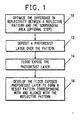
- a method of forming an electronic microcircuit including forming a pattern of metallic electrical conductors on the surface of a substcate and covering the remainder of the substrate surface but not the conductors with a resist, is characterised by coating the substrate surface with a positive acting photoresist which is responsive to actinic radiation in a wavelength band which is reflected substantially more by the metallic conductors than the remainder of the substrate surface, blanket exposing the photoresist with said radiation, thus causing greater exposure of the areas of photoresist overlying the metallic conductors than the areas of photoresist overlying the remainder of the substrate surface, and developing the blanket exposed photoresist to remove the areas of photoresist overlying the conductors.
- a method of forming an electronic microcircuit including forming a pattern of metallic electrical conductors on the surface of a substrate and covering the conductors but not the remainder of the substrate surface with a resist, is characterised by coating the substrate surface with a negative acting photoresist which is responsive to actinic radiation in a wavelength band which is reflected substantially more by the metallic conductors than the remainder of the substrate surface, blanket exposing the photoresist with said radiation, thus causing greater exposure of the areas of photoresist overlying the metallic conductors than the areas of photoresist overlying the remainder of the substrate surface, and developing the blanket exposed photoresist to remove the areas of photoresist overlying the remainder of the substrate surface.
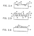
- a substrate 20 (Fig. 2.1) carries a metallic pattern 22 which is to be selectively coated with another material.
- This step typically occurs, for example, in multi-layer ceramic integrated circuit technology, where ceramic sheets are patterned with metallic paste, laminated and fired. Better adhesion characteristics are typically desired for the metallic pattern areas which are to be contacted with solder, so that it becomes desirable to be able to deposit additional (and typically different) metal on the top metallic pattern of a multi-layer ceramic substrate.
- a second step 12 the polished metallic pattern is covered with a layer of photoresist 24 (Fig. 2.2).
- photoresist 24 Any suitable photoresist may be used, such as AZ 1350 (AZ is a trademark of the Shipley Co.).
- AZ 1350 AZ is a trademark of the Shipley Co.
- a positive photoresist is described. It should be apparent that a negative photoresist could alternatively be used as well to obtain a complementary self-aligned resist pattern.
- the deposited resist layer is next blanket or flood exposed 14 (Fig. 1) to actinic radiation, such as ultraviolet light.
- actinic radiation such as ultraviolet light.
- the UV light passes through the photoresist layer 24 and is largely reflected back upwards through the resist layer by the metallic pattern 22. In the less reflective regions outside the metallic pattern, the UV light largely passes into the substrate 20 and is absorbed.
- Fig. 2.3 What has been illustrated in Fig. 2.3 is the ideal situation where the reflective pattern 22 totally reflects UV light (represented by the up turned arrows) and the non-reflective areas totally absorb UV light (represented by the arrows penetrating the substrate 20). In a practical situation UV light is partly reflected and partly absorbed in both regions, but the more highly reflective pattern reflects much more of the UV light than does the less reflective surrounding area. A difference in exposure thus results with respect to photoresist regions 26 overlying more highly reflective areas in comparison with photoresist regions 28 overlying less highly reflective areas.
- the more highly exposed resist regions overlying relatively more reflective areas dissolve more readily in a developer solution than do the less highly exposed resist regions overlying relatively less reflective areas.
- the degree to which this difference in dissolution rate occurs with respect to a given difference in exposure is referred to as the contrast of the resist.
- a high contrast resist may be used in order to reduce the need for a very high difference in reflectivity.
- a higher resist contrast will reduce the amount of resist thickness lost in the less highly exposed regions during complete development of the more highly exposed regions.
- the initial resist layer thickness need not be as great and better resolution occurs.
- the exposed resist layer is developed to the point where the more highly exposed regions 26 have been completely dissolved away (Fig. 2.4), leaving a resist pattern 30 consisting of the less highly exposed regions 28.
- the resulting resist pattern is the complement of and is perfectly aligned with the metallic pattern 22.
- the self-aligned corresponding resist pattern may now be used in any manner and for any purpose that resist patterns are used. It may be used to selectively deposit material by an evaporation or plating or sputtering technique, for example. Also, it may be used to selectively remove material by any suitable process such as by chemical or ion etching for the purpose of cleaning or polishing or for some other purpose. Alternatively it may be used to selectively modify the exposed regions, for example by chemical treatment or by ion bombardment.
- a metallic layer 32 has been evaporated over the resist pattern.
- the metallic layer covers the underlying reflective pattern 22 (regions 34) as well as the resist pattern 30 (regions 36) and has intermediate discontinuity.
- the resist pattern 30 is removed (Fig. 2.6)
- the metallic layer regions 36 overlying the resist pattern are also removed (a lift-off process), leaving the original pattern 22 now covered with an identical and aligned metallic pattern 38 consisting of regions 34.
- a negative photoresist would selectively cover the metallic pattern so that the complementary less reflective regions could be preferentially treated instead of the more reflective regions. This might be used, for example, to etch or clean the less reflective regions or to modify the edge profile of the reflective pattern in order to decrease the overcut or increase the undercut of the edge profile.
Landscapes
- Engineering & Computer Science (AREA)
- Manufacturing & Machinery (AREA)
- Microelectronics & Electronic Packaging (AREA)
- Physics & Mathematics (AREA)
- General Physics & Mathematics (AREA)
- Exposure And Positioning Against Photoresist Photosensitive Materials (AREA)
- Manufacturing Of Printed Wiring (AREA)
- Internal Circuitry In Semiconductor Integrated Circuit Devices (AREA)
- Weting (AREA)
- Exposure Of Semiconductors, Excluding Electron Or Ion Beam Exposure (AREA)
Claims (7)
Applications Claiming Priority (2)
| Application Number | Priority Date | Filing Date | Title |
|---|---|---|---|
| US06/336,467 US4379833A (en) | 1981-12-31 | 1981-12-31 | Self-aligned photoresist process |
| US336467 | 1981-12-31 |
Publications (3)
| Publication Number | Publication Date |
|---|---|
| EP0083397A2 EP0083397A2 (de) | 1983-07-13 |
| EP0083397A3 EP0083397A3 (en) | 1986-06-04 |
| EP0083397B1 true EP0083397B1 (de) | 1989-04-12 |
Family
ID=23316216
Family Applications (1)
| Application Number | Title | Priority Date | Filing Date |
|---|---|---|---|
| EP82109507A Expired EP0083397B1 (de) | 1981-12-31 | 1982-10-14 | Verfahren zur Herstellung von elektronischen Mikroschaltkreisstruckturen |
Country Status (4)
| Country | Link |
|---|---|
| US (1) | US4379833A (de) |
| EP (1) | EP0083397B1 (de) |
| JP (1) | JPS58119640A (de) |
| DE (1) | DE3279612D1 (de) |
Families Citing this family (25)
| Publication number | Priority date | Publication date | Assignee | Title |
|---|---|---|---|---|
| US4576832A (en) * | 1982-12-30 | 1986-03-18 | International Business Machines Corporation | Self-aligning mask |
| US4564584A (en) * | 1983-12-30 | 1986-01-14 | Ibm Corporation | Photoresist lift-off process for fabricating semiconductor devices |
| US4672023A (en) * | 1985-10-21 | 1987-06-09 | Avantek, Inc. | Method for planarizing wafers |
| JPS62177187A (ja) * | 1986-01-30 | 1987-08-04 | Sumitomo Suriim Kk | 金属画像の形成方法 |
| US5352559A (en) * | 1987-07-10 | 1994-10-04 | Sharp Kabushiki Kaisha | Photosensitive sheet and a method for the formation of images using the same |
| JPH01125929A (ja) * | 1987-11-11 | 1989-05-18 | Toshiba Corp | フォトレジストのパターン形成方法 |
| US5208066A (en) * | 1989-03-18 | 1993-05-04 | Hitachi, Ltd. | Process of forming a patterned polyimide film and articles including such a film |
| KR0119377B1 (ko) * | 1993-12-10 | 1997-09-30 | 김주용 | 반도체장치 제조방법 |
| KR970007173B1 (ko) * | 1994-07-14 | 1997-05-03 | 현대전자산업 주식회사 | 미세패턴 형성방법 |
| US5879866A (en) * | 1994-12-19 | 1999-03-09 | International Business Machines Corporation | Image recording process with improved image tolerances using embedded AR coatings |
| JPH09244253A (ja) * | 1996-03-05 | 1997-09-19 | Nitto Boseki Co Ltd | パターン形成方法 |
| US5935763A (en) * | 1996-06-11 | 1999-08-10 | International Business Machines Corporation | Self-aligned pattern over a reflective layer |
| US5981150A (en) * | 1996-07-05 | 1999-11-09 | Kabushiki Kaisha Toshiba | Method for forming a resist pattern |
| US5952156A (en) * | 1997-07-11 | 1999-09-14 | Vanguard International Semiconductor Corporation | Enhanced reflectivity coating (ERC) for narrow aperture width contact and interconnection lithography |
| RU2145156C1 (ru) * | 1999-02-09 | 2000-01-27 | Нижегородский государственный технический университет | Способ формирования структур в микроэлектронике |
| KR100301818B1 (ko) * | 1999-06-29 | 2001-11-01 | 김영환 | 셀프 얼라인 포토리소그래피 및 그를 이용한 반도체 소자 제조방법 |
| US6485894B1 (en) * | 2000-09-29 | 2002-11-26 | International Business Machines Corporation | Method to self-align a lithographic pattern to a workpiece |
| DE10128481B4 (de) * | 2001-06-12 | 2004-01-08 | Infineon Technologies Ag | Verfahren zur Ätzung eines Substrats |
| DE10137830A1 (de) | 2001-08-02 | 2003-02-27 | Infineon Technologies Ag | Verfahren zum Herstellen einer selbstjustierten Struktur auf einem Halbleiter-Wafer |
| US20030059718A1 (en) * | 2001-09-24 | 2003-03-27 | Koninklijke Philips Electronics N.V. | Method for forming a contact window in a semiconductor device |
| US6849388B2 (en) * | 2002-10-22 | 2005-02-01 | Northrop Grumman Corporation | Self-aligning contacts for stacked electronics |
| US20050257709A1 (en) * | 2003-08-28 | 2005-11-24 | Tony Mule | Systems and methods for three-dimensional lithography and nano-indentation |
| JP2005285308A (ja) * | 2004-03-02 | 2005-10-13 | Tdk Corp | 薄膜処理方法及び薄膜磁気ヘッドの製造方法 |
| EP2736076A1 (de) * | 2012-11-23 | 2014-05-28 | Nederlandse Organisatie voor toegepast -natuurwetenschappelijk onderzoek TNO | Vorrichtung und Verfahren zur Herstellung eines geschichteten Produktes |
| CN114460819B (zh) * | 2022-01-14 | 2024-01-26 | 北京量子信息科学研究院 | 用于电子束曝光的对准标记及其制备方法 |
Family Cites Families (5)
| Publication number | Priority date | Publication date | Assignee | Title |
|---|---|---|---|---|
| JPS5145475A (en) * | 1974-10-15 | 1976-04-17 | Kogyo Gijutsuin | Toshigomino ekikashorihoho |
| US4001061A (en) * | 1975-03-05 | 1977-01-04 | International Business Machines Corporation | Single lithography for multiple-layer bubble domain devices |
| DE2658400A1 (de) * | 1976-12-23 | 1978-06-29 | Ibm Deutschland | Verfahren zur herstellung einer negativen maske auf einem substrat |
| JPS55153938A (en) * | 1979-05-18 | 1980-12-01 | Sharp Corp | Image forming material for contact reflection exposure |
| US4293624A (en) * | 1979-06-26 | 1981-10-06 | The Perkin-Elmer Corporation | Method for making a mask useful in X-ray lithography |
-
1981
- 1981-12-31 US US06/336,467 patent/US4379833A/en not_active Expired - Lifetime
-
1982
- 1982-10-14 EP EP82109507A patent/EP0083397B1/de not_active Expired
- 1982-10-14 DE DE8282109507T patent/DE3279612D1/de not_active Expired
- 1982-10-19 JP JP57182220A patent/JPS58119640A/ja active Pending
Also Published As
| Publication number | Publication date |
|---|---|
| US4379833A (en) | 1983-04-12 |
| EP0083397A3 (en) | 1986-06-04 |
| JPS58119640A (ja) | 1983-07-16 |
| EP0083397A2 (de) | 1983-07-13 |
| DE3279612D1 (en) | 1989-05-18 |
Similar Documents
| Publication | Publication Date | Title |
|---|---|---|
| EP0083397B1 (de) | Verfahren zur Herstellung von elektronischen Mikroschaltkreisstruckturen | |
| US4202914A (en) | Method of depositing thin films of small dimensions utilizing silicon nitride lift-off mask | |
| US3982943A (en) | Lift-off method of fabricating thin films and a structure utilizable as a lift-off mask | |
| US4115120A (en) | Method of forming thin film patterns by differential pre-baking of resist | |
| CA1123118A (en) | Fabrication of integrated circuits utilizing thick high-resolution patterns | |
| US4328298A (en) | Process for manufacturing lithography masks | |
| US4218532A (en) | Photolithographic technique for depositing thin films | |
| US4174219A (en) | Method of making a negative exposure mask | |
| US5840622A (en) | Phase mask laser fabrication of fine pattern electronic interconnect structures | |
| US3510371A (en) | Method of making an ultraviolet sensitive template | |
| US4451554A (en) | Method of forming thin-film pattern | |
| EP0401314B1 (de) | Kryogenes verfahren für metallabzug | |
| EP0134789B1 (de) | Zweischichten-uv-empfindliches schutzsystem für strukturierung von hochreflektiven trägern | |
| US3986876A (en) | Method for making a mask having a sloped relief | |
| JPS62142323A (ja) | X線ホトリソグラフイに使用するマスクの加法的方法及びその結果得られるマスク | |
| JPH0466345B2 (de) | ||
| US6686128B1 (en) | Method of fabricating patterned layers of material upon a substrate | |
| KR0162967B1 (ko) | 알루미나 기판 상에 박/후막 저항을 동시에 제조하는 방법 | |
| JP2705253B2 (ja) | 導体パターン形成方法と磁気ヘッドの製造方法 | |
| US3951659A (en) | Method for resist coating of a glass substrate | |
| JPH02156244A (ja) | パターン形成方法 | |
| JPH02138468A (ja) | パターン形成法 | |
| JPS604221A (ja) | 半導体装置の製造方法 | |
| JP2580681B2 (ja) | 半導体装置の製造方法 | |
| KR0177869B1 (ko) | 고해상도 포토리소그래피 방법 및 구조 |
Legal Events
| Date | Code | Title | Description |
|---|---|---|---|
| PUAI | Public reference made under article 153(3) epc to a published international application that has entered the european phase |
Free format text: ORIGINAL CODE: 0009012 |
|
| AK | Designated contracting states |
Designated state(s): DE FR GB |
|
| 17P | Request for examination filed |
Effective date: 19831021 |
|
| PUAL | Search report despatched |
Free format text: ORIGINAL CODE: 0009013 |
|
| AK | Designated contracting states |
Kind code of ref document: A3 Designated state(s): DE FR GB |
|
| 17Q | First examination report despatched |
Effective date: 19880729 |
|
| GRAA | (expected) grant |
Free format text: ORIGINAL CODE: 0009210 |
|
| AK | Designated contracting states |
Kind code of ref document: B1 Designated state(s): DE FR GB |
|
| REF | Corresponds to: |
Ref document number: 3279612 Country of ref document: DE Date of ref document: 19890518 |
|
| ET | Fr: translation filed | ||
| PLBE | No opposition filed within time limit |
Free format text: ORIGINAL CODE: 0009261 |
|
| STAA | Information on the status of an ep patent application or granted ep patent |
Free format text: STATUS: NO OPPOSITION FILED WITHIN TIME LIMIT |
|
| 26N | No opposition filed | ||
| PGFP | Annual fee paid to national office [announced via postgrant information from national office to epo] |
Ref country code: GB Payment date: 19910923 Year of fee payment: 10 |
|
| PGFP | Annual fee paid to national office [announced via postgrant information from national office to epo] |
Ref country code: FR Payment date: 19911001 Year of fee payment: 10 |
|
| PGFP | Annual fee paid to national office [announced via postgrant information from national office to epo] |
Ref country code: DE Payment date: 19911102 Year of fee payment: 10 |
|
| PG25 | Lapsed in a contracting state [announced via postgrant information from national office to epo] |
Ref country code: GB Effective date: 19921014 |
|
| GBPC | Gb: european patent ceased through non-payment of renewal fee |
Effective date: 19921014 |
|
| PG25 | Lapsed in a contracting state [announced via postgrant information from national office to epo] |
Ref country code: FR Effective date: 19930630 |
|
| PG25 | Lapsed in a contracting state [announced via postgrant information from national office to epo] |
Ref country code: DE Effective date: 19930701 |
|
| REG | Reference to a national code |
Ref country code: FR Ref legal event code: ST |