EP0083531A1 - Gunndiodenähnliche unipolare Anordnung mit Elektronentransfer - Google Patents
Gunndiodenähnliche unipolare Anordnung mit Elektronentransfer Download PDFInfo
- Publication number
- EP0083531A1 EP0083531A1 EP82402367A EP82402367A EP0083531A1 EP 0083531 A1 EP0083531 A1 EP 0083531A1 EP 82402367 A EP82402367 A EP 82402367A EP 82402367 A EP82402367 A EP 82402367A EP 0083531 A1 EP0083531 A1 EP 0083531A1
- Authority
- EP
- European Patent Office
- Prior art keywords
- layer
- contact
- transit
- undoped
- substrate
- Prior art date
- Legal status (The legal status is an assumption and is not a legal conclusion. Google has not performed a legal analysis and makes no representation as to the accuracy of the status listed.)
- Granted
Links
- 230000027756 respiratory electron transport chain Effects 0.000 title claims abstract description 7
- 239000000463 material Substances 0.000 claims abstract description 26
- 238000002347 injection Methods 0.000 claims abstract description 15
- 239000007924 injection Substances 0.000 claims abstract description 15
- 230000004888 barrier function Effects 0.000 claims abstract description 13
- 239000000758 substrate Substances 0.000 claims abstract description 12
- 238000001465 metallisation Methods 0.000 claims abstract description 10
- 230000000694 effects Effects 0.000 claims abstract description 9
- 239000004065 semiconductor Substances 0.000 claims abstract description 5
- 229910001218 Gallium arsenide Inorganic materials 0.000 claims description 15
- 239000000203 mixture Substances 0.000 claims description 4
- 230000005684 electric field Effects 0.000 description 5
- 239000000243 solution Substances 0.000 description 5
- 230000007935 neutral effect Effects 0.000 description 4
- 239000002131 composite material Substances 0.000 description 3
- 150000001875 compounds Chemical class 0.000 description 3
- 238000009825 accumulation Methods 0.000 description 2
- 230000015572 biosynthetic process Effects 0.000 description 2
- 230000000903 blocking effect Effects 0.000 description 2
- 230000007423 decrease Effects 0.000 description 2
- 238000010586 diagram Methods 0.000 description 2
- 238000005516 engineering process Methods 0.000 description 2
- 238000000407 epitaxy Methods 0.000 description 2
- 230000007246 mechanism Effects 0.000 description 2
- 230000008261 resistance mechanism Effects 0.000 description 2
- 230000003068 static effect Effects 0.000 description 2
- 230000005641 tunneling Effects 0.000 description 2
- 229910000980 Aluminium gallium arsenide Inorganic materials 0.000 description 1
- 229910017398 Au—Ni Inorganic materials 0.000 description 1
- 230000003321 amplification Effects 0.000 description 1
- 230000002238 attenuated effect Effects 0.000 description 1
- 239000000969 carrier Substances 0.000 description 1
- 238000013016 damping Methods 0.000 description 1
- 230000007547 defect Effects 0.000 description 1
- 230000005284 excitation Effects 0.000 description 1
- 238000002474 experimental method Methods 0.000 description 1
- 238000001451 molecular beam epitaxy Methods 0.000 description 1
- 238000003199 nucleic acid amplification method Methods 0.000 description 1
- 230000000704 physical effect Effects 0.000 description 1
- 238000005498 polishing Methods 0.000 description 1
- 230000001902 propagating effect Effects 0.000 description 1
- 238000004088 simulation Methods 0.000 description 1
Images


Classifications
-
- H—ELECTRICITY
- H10—SEMICONDUCTOR DEVICES; ELECTRIC SOLID-STATE DEVICES NOT OTHERWISE PROVIDED FOR
- H10N—ELECTRIC SOLID-STATE DEVICES NOT OTHERWISE PROVIDED FOR
- H10N80/00—Bulk negative-resistance effect devices
- H10N80/10—Gunn-effect devices
- H10N80/107—Gunn diodes
Definitions
- the invention relates to an electron transfer diode, and more precisely a new cathode structure for this type of diode, more commonly called the Gunn diode.
- the object of this new cathode is to increase the useful power of the diode and to extend the operating range in the microwave domain.
- Gunn diodes are microwave generation or amplification components whose operation is based on a negative volume resistance mechanism, inherent in certain compounds of the III-V family, in particular GaAs and InP, among others.
- a Gunn diode critically depends on the boundary conditions at the cathode.
- the nature of the cathodic contact and the structure of the region contiguous to this contact have very significant repercussions on the mode of operation of the device as well as on the functional characteristics of the latter in electrical efficiency, power, frequency range, noise, etc. ...
- the conduction band of III-V compounds such as GaAs or InP has two valleys, sometimes three, but we will limit our to the simpler model of two valleys : the main valley in which the electrons are very mobile ( / u> 5000 cm2 / V / s for an N doping concentration d ⁇ 10 15 cm -3 ) and the secondary valley in which the mobility is about 20 times lower.
- the secondary minimum is located, in the energy scale, a few tenths of electron volts (0.35 eV for GaAs, 0.5 eV for InP) above the main minimum.
- ⁇ d being the differential conductivity
- ⁇ the dielectric constant of the medium
- the growth rate ⁇ d / ⁇ is related to the dielectric relaxation, - which corresponds to a negative damping since ⁇ d ⁇ 0, while propagating from the cathode towards the anode at the average speed of the carriers. It is therefore a convective instability, the characteristics of which depend not only on the physical properties of the material, but also, very critically, on the initial conditions, that is to say the injection conditions at the cathode.
- the cathode structure proposed is a different solution to the same problem, to which the invention provides a simple solution in its foundation and in its implementation. It achieves the proper injection characteristics. Its technology, based on molecular beam epitaxy for example, is particularly well suited to structures requiring good definition.
- the invention consists of a unipolar electron transfer device, of the Gunn diode type, operating in the microwave domain, the semiconductor body of which comprises a contact layer, carrying a first metallization for picking up contact, this layer being made of a first highly doped material, of polarity n + and a transit layer made of the same material, less doped of polarity n, these two layers being supported by a buffer layer and by a substrate, of the same material and of the same doping as the contact layer, the substrate constituting the anodic contact of the device and supporting a second metallization of contact making, this device being characterized in that the injection of electrons from the contact layer towards the transit layer is produced by tunnel effect through a double heterojunction consisting of a layer, of a second material, undoped, having a tunnel barrier in the band of co nduction, this undoped layer being interposed between the contact layer and the transit layer.
- the injecting contact brings an excess of electronic density compared to the density of donors.
- the ohmic contact or the n + n junction are typical examples.
- FIG. 1 represents the characteristics of a cathodic contact, and gives the different curves of current density J as a function of the cathodic field E, for the injecting contacts, and the limiting contacts.
- the properties of a Gunn diode are improved if the cathode contact is limiting, but also if the so-called "dead" area in front of the cathode is as short as possible.
- the dead zone has a thickness of the order of magnitude of the distance that an electron must travel from the cathode, before being sufficiently "heated” by the electric field for the transfer in the upper valley to occur.
- the dead zone constitutes an additional access resistance. It should be as thin as possible, especially for the highest frequencies where the extension of the transit region becomes of the same order of magnitude.
- the electric field at the cathode must be as large as possible, which led to experiment with a Schottky contact with low barrier or a composite cathode whose ohmic contact is followed by a structure composed of a lightly doped layer and then a thin, highly doped layer, forming a barrier.
- the low barrier Schottky cathode does not appear to be very industrial due to poor reproducibility, and the composite cathode has given excellent results, but its sophisticated technology seems to be of little industrial nature.
- FIG. 2 shows a sectional view of a Gunn diode according to the invention. This figure is shown schematically in order to highlight the structure of the semiconductor layers rather than the actual geometry of the diode.
- the substrate 9 is made of monocrystalline material which has undergone prior sawing and polishing operations: this has resulted in imperfections on its surface in the crystallographic network.
- the function of the buffer layer 8, which is deposited by epitaxy, is to repair these crystallographic imperfections, which are attenuated as new layers of atoms of the material are deposited.
- the diode is supplemented by two metallizations which constitute ohmic contacts, the metallization 10 of cathodic contact and the metallization 11 of anodic contact. These ohmic contacts are made, for example, by the Ge-Au-Ni chain.
- the doping levels are of the order of 10 18 atoms.cm -3 for the n layers, and of the order of 1.5 to 2.10 15 atoms.cm -3 for the n layer at 10 GHz, although for the latter the doping level reaches 10 16 to 100 GHz.
- the diode according to the invention is composed only of layers of polarity n that it is said to be unipolar.
- a similar diode of polarity only p is not possible, because the holes do not present the same phenomenon of valleys and negative slope as the electrons.
- FIGS. 3 and 4 show the diagrams of conduction bands of the structure according to the invention.
- the energy at the bottom of the conduction band is represented there as a function of the distance, that is to say in the different layers of the diode, for an applied voltage Vd zero on the anode in FIG. 3 and for a positive voltage Vd in FIG. 4.
- the energy level of Fermi E F is taken as the reference level.
- FIG. 3 therefore gives the energy levels of the different layers, in the static state, out of any excitation by a potential.
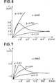
- the cathode characteristic that is to say the tunnel current J (V K ) was determined by simulation. This shows that by playing on ⁇ , that is to say on the stoichiometry of the compound Al x Ga 1 As, and on the thickness "a" of the layer, it is possible to obtain conditions d 'injection of suitable current, with values of ⁇ and "a” which are compatible with the technological possibilities, and taking into account the tunnel effect assisted by the temperature as well as the pure thermionic effect.
- the neutral characteristic has been shown in the same figures, which makes it possible to distinguish the three injection regimes.
- the influence of the height of barrier réelle is very sensitive, from where the interest of the epitaxy by molecular jets allowing a precise control of the stoichiometry of Al x Ga 1-x As.
- the thickness "a" of the undoped layer 6 has little influence on the characteristic J K (E K ) which means that the field at the cathode is almost identical for the three cases. It is not the same for the potential V K applied to the layer, that is to say the energy qV K of the electron emitted by the cathode, VK being proportional to "a". It is therefore preferable, to reduce the dead zone, to choose "a" large, of the order of 1000 A or more. The limit is due on the one hand to the maximum acceptable value for V K which must remain low compared to the voltage Vd on the diode, on the other hand to the fact that the influence of ⁇ on the characteristics of injection is of as much more sensitive as "a” is greater.
- the exemplary embodiment of Gunn diode which has been exposed by relying on the pair of material GaAs / Al x Ga 1-x As is not limiting of the invention, and can be extended to other pairs of semiconductor materials, such as:
- compositions of these materials are chosen such that the crystalline parameter of each pair of materials is equal and that the discontinuity in their conduction bands defines a barrier height as indicated.
Landscapes
- Electrodes Of Semiconductors (AREA)
- Radar Systems Or Details Thereof (AREA)
- Apparatus For Radiation Diagnosis (AREA)
Applications Claiming Priority (2)
| Application Number | Priority Date | Filing Date | Title |
|---|---|---|---|
| FR8124568 | 1981-12-31 | ||
| FR8124568A FR2519473A1 (fr) | 1981-12-31 | 1981-12-31 | Dispositif unipolaire a transfert d'electrons du type diode gunn |
Publications (2)
| Publication Number | Publication Date |
|---|---|
| EP0083531A1 true EP0083531A1 (de) | 1983-07-13 |
| EP0083531B1 EP0083531B1 (de) | 1985-05-22 |
Family
ID=9265568
Family Applications (1)
| Application Number | Title | Priority Date | Filing Date |
|---|---|---|---|
| EP82402367A Expired EP0083531B1 (de) | 1981-12-31 | 1982-12-23 | Gunndiodenähnliche unipolare Anordnung mit Elektronentransfer |
Country Status (4)
| Country | Link |
|---|---|
| EP (1) | EP0083531B1 (de) |
| JP (1) | JPS58122791A (de) |
| DE (1) | DE3263795D1 (de) |
| FR (1) | FR2519473A1 (de) |
Cited By (2)
| Publication number | Priority date | Publication date | Assignee | Title |
|---|---|---|---|---|
| FR2604573A1 (fr) * | 1986-09-26 | 1988-04-01 | Gen Electric Co Plc | Dispositif electronique generateur d'oscillations coherentes |
| EP0343737A3 (de) * | 1988-05-27 | 1991-01-02 | Philips Electronics Uk Limited | Bauelement unter Benutzung des Elektronentransfereffektes |
Families Citing this family (2)
| Publication number | Priority date | Publication date | Assignee | Title |
|---|---|---|---|---|
| JP3578381B2 (ja) * | 1998-03-25 | 2004-10-20 | シャープ株式会社 | ガンダイオード |
| DE10261238A1 (de) * | 2002-12-20 | 2004-07-15 | Forschungszentrum Jülich GmbH | Schichtenfolge |
Citations (2)
| Publication number | Priority date | Publication date | Assignee | Title |
|---|---|---|---|---|
| GB1434308A (en) * | 1973-05-31 | 1976-05-05 | Standard Telephones Cables Ltd | Semiconductor devices |
| FR2293067A1 (fr) * | 1974-11-29 | 1976-06-25 | Thomson Csf | Cathode pour diode de gunn et diode de gunn comportant une telle cathode |
Family Cites Families (1)
| Publication number | Priority date | Publication date | Assignee | Title |
|---|---|---|---|---|
| FR2515866A1 (fr) * | 1981-10-30 | 1983-05-06 | Thomson Csf | Dispositif a transfert d'electrons fonctionnant le domaine des hyperfrequences |
-
1981
- 1981-12-31 FR FR8124568A patent/FR2519473A1/fr active Granted
-
1982
- 1982-12-23 EP EP82402367A patent/EP0083531B1/de not_active Expired
- 1982-12-23 DE DE8282402367T patent/DE3263795D1/de not_active Expired
- 1982-12-28 JP JP57234970A patent/JPS58122791A/ja active Pending
Patent Citations (2)
| Publication number | Priority date | Publication date | Assignee | Title |
|---|---|---|---|---|
| GB1434308A (en) * | 1973-05-31 | 1976-05-05 | Standard Telephones Cables Ltd | Semiconductor devices |
| FR2293067A1 (fr) * | 1974-11-29 | 1976-06-25 | Thomson Csf | Cathode pour diode de gunn et diode de gunn comportant une telle cathode |
Non-Patent Citations (1)
| Title |
|---|
| IBM TECHNICAL DISCLOSURE BULLETIN, vol. 24, no. 7B, décembre 1981, pages 3701-3702, New York, US * |
Cited By (2)
| Publication number | Priority date | Publication date | Assignee | Title |
|---|---|---|---|---|
| FR2604573A1 (fr) * | 1986-09-26 | 1988-04-01 | Gen Electric Co Plc | Dispositif electronique generateur d'oscillations coherentes |
| EP0343737A3 (de) * | 1988-05-27 | 1991-01-02 | Philips Electronics Uk Limited | Bauelement unter Benutzung des Elektronentransfereffektes |
Also Published As
| Publication number | Publication date |
|---|---|
| FR2519473A1 (fr) | 1983-07-08 |
| EP0083531B1 (de) | 1985-05-22 |
| JPS58122791A (ja) | 1983-07-21 |
| FR2519473B1 (de) | 1985-05-17 |
| DE3263795D1 (en) | 1985-06-27 |
Similar Documents
| Publication | Publication Date | Title |
|---|---|---|
| EP0017531B1 (de) | Feldeffekttransistor mit hoher Grenzfrequenz und Verfahren zu dessen Herstellung | |
| EP2715808B1 (de) | Halbleiterstruktur zur ausstrahlung von licht und verfahren zur herstellung einer solchen struktur | |
| EP0236189B1 (de) | Monolithische Halbleiterstruktur eines Bipoltransistors mit Heteroübergängen und eines Lasers | |
| EP3203526B1 (de) | Transistor mit heteroübergang mit verbessertem elektronengas-einschluss | |
| FR2490874A1 (fr) | Transistors du type a grille isolee | |
| EP2337094B1 (de) | Eine auf Rekombination von lokalisierten Exzitonen basierende Photonquelle | |
| EP0084393A2 (de) | Hetero-Übergangstransistor Halbleiteranordnung | |
| FR2517888A1 (fr) | Dispositif a semi-conducteur comportant une structure de grille associee a une jonction de faible profondeur | |
| EP1243029B1 (de) | Heteroübergang-Bipolartransistor mit obenliegendem Kollektor und dessen Herstellungsverfahren | |
| EP0001374A1 (de) | Metallbasistransistor mit unkristallinischen Dünnschichten aus Halbleitern | |
| FR2745421A1 (fr) | Mesfet du type enrichissement | |
| EP0070211A1 (de) | Ballistischer Transistor mit mehreren Heteroübergängen | |
| EP0051504B1 (de) | Feldeffekttransistor mit einem kurzen Kanal | |
| FR2568410A1 (fr) | Transistor statique a induction et son circuit integre | |
| EP0522952B1 (de) | Feldeffekt-Transistor mit dünnen Barrierenschichten und einer dünnen, dotierten Schicht | |
| EP0145567B1 (de) | Feldeffekttransistor mit vertikaler Struktur | |
| EP0232662B1 (de) | Monolithische Halbleiterstruktur bestehend aus einem Laser und einem Feldeffekttransistor und deren Herstellungsverfahren | |
| EP0083531B1 (de) | Gunndiodenähnliche unipolare Anordnung mit Elektronentransfer | |
| EP0684653B1 (de) | Lichtgesteuerter Heterostruktur-Halbleiterbaustein zur Erzeugung von Mikrowellen | |
| FR2496990A1 (fr) | Transistor a effet de champ a barriere schottky | |
| FR2569056A1 (fr) | Transistor a induction statique du type a injection par effet tunnel et circuit integre comprenant un tel transistor | |
| FR2604573A1 (fr) | Dispositif electronique generateur d'oscillations coherentes | |
| EP0078726B1 (de) | Anordnung mit Elektronentransfer im Mikrowellenbereich arbeitend | |
| EP0027761A1 (de) | Hochfrequenz-Feldeffekt-Halbleitervorrichtung und Transistor, die eine solche Halbleitervorrichtung verwenden | |
| FR2471050A1 (fr) | Dispositifs semi-conducteurs a effet de champ |
Legal Events
| Date | Code | Title | Description |
|---|---|---|---|
| PUAI | Public reference made under article 153(3) epc to a published international application that has entered the european phase |
Free format text: ORIGINAL CODE: 0009012 |
|
| AK | Designated contracting states |
Designated state(s): DE GB NL |
|
| 17P | Request for examination filed |
Effective date: 19830722 |
|
| GRAA | (expected) grant |
Free format text: ORIGINAL CODE: 0009210 |
|
| AK | Designated contracting states |
Designated state(s): DE GB NL |
|
| REF | Corresponds to: |
Ref document number: 3263795 Country of ref document: DE Date of ref document: 19850627 |
|
| PLBE | No opposition filed within time limit |
Free format text: ORIGINAL CODE: 0009261 |
|
| STAA | Information on the status of an ep patent application or granted ep patent |
Free format text: STATUS: NO OPPOSITION FILED WITHIN TIME LIMIT |
|
| 26N | No opposition filed | ||
| PG25 | Lapsed in a contracting state [announced via postgrant information from national office to epo] |
Ref country code: NL Effective date: 19860701 |
|
| NLV4 | Nl: lapsed or anulled due to non-payment of the annual fee | ||
| PG25 | Lapsed in a contracting state [announced via postgrant information from national office to epo] |
Ref country code: DE Effective date: 19860902 |
|
| GBPC | Gb: european patent ceased through non-payment of renewal fee | ||
| PG25 | Lapsed in a contracting state [announced via postgrant information from national office to epo] |
Ref country code: GB Free format text: LAPSE BECAUSE OF NON-PAYMENT OF DUE FEES Effective date: 19881122 |