EP0084000A2 - CMOS Anordnung - Google Patents
CMOS Anordnung Download PDFInfo
- Publication number
- EP0084000A2 EP0084000A2 EP83400013A EP83400013A EP0084000A2 EP 0084000 A2 EP0084000 A2 EP 0084000A2 EP 83400013 A EP83400013 A EP 83400013A EP 83400013 A EP83400013 A EP 83400013A EP 0084000 A2 EP0084000 A2 EP 0084000A2
- Authority
- EP
- European Patent Office
- Prior art keywords
- source
- cmos device
- conductivity type
- terminal
- substrate
- Prior art date
- Legal status (The legal status is an assumption and is not a legal conclusion. Google has not performed a legal analysis and makes no representation as to the accuracy of the status listed.)
- Withdrawn
Links
- 239000000758 substrate Substances 0.000 claims description 36
- 239000002019 doping agent Substances 0.000 claims description 8
- 239000004065 semiconductor Substances 0.000 claims description 8
- 230000000295 complement effect Effects 0.000 claims description 2
- 230000003071 parasitic effect Effects 0.000 abstract description 32
- 230000003247 decreasing effect Effects 0.000 abstract description 5
- 108091006146 Channels Proteins 0.000 description 23
- 238000010586 diagram Methods 0.000 description 8
- XUIMIQQOPSSXEZ-UHFFFAOYSA-N Silicon Chemical compound [Si] XUIMIQQOPSSXEZ-UHFFFAOYSA-N 0.000 description 5
- 229910052710 silicon Inorganic materials 0.000 description 5
- 239000010703 silicon Substances 0.000 description 5
- 230000036039 immunity Effects 0.000 description 4
- 238000000034 method Methods 0.000 description 4
- 235000009374 Basella Nutrition 0.000 description 2
- 241000219301 Basella Species 0.000 description 2
- 108010075750 P-Type Calcium Channels Proteins 0.000 description 1
- 238000004458 analytical method Methods 0.000 description 1
- 238000010276 construction Methods 0.000 description 1
- 230000007423 decrease Effects 0.000 description 1
- 230000007547 defect Effects 0.000 description 1
- 238000009792 diffusion process Methods 0.000 description 1
- 230000008030 elimination Effects 0.000 description 1
- 238000003379 elimination reaction Methods 0.000 description 1
- 238000005516 engineering process Methods 0.000 description 1
- 238000003780 insertion Methods 0.000 description 1
- 230000037431 insertion Effects 0.000 description 1
- 238000004519 manufacturing process Methods 0.000 description 1
- 229910044991 metal oxide Inorganic materials 0.000 description 1
- 150000004706 metal oxides Chemical class 0.000 description 1
- 230000002265 prevention Effects 0.000 description 1
- 239000002699 waste material Substances 0.000 description 1
Images


Classifications
-
- H—ELECTRICITY
- H10—SEMICONDUCTOR DEVICES; ELECTRIC SOLID-STATE DEVICES NOT OTHERWISE PROVIDED FOR
- H10D—INORGANIC ELECTRIC SEMICONDUCTOR DEVICES
- H10D84/00—Integrated devices formed in or on semiconductor substrates that comprise only semiconducting layers, e.g. on Si wafers or on GaAs-on-Si wafers
- H10D84/80—Integrated devices formed in or on semiconductor substrates that comprise only semiconducting layers, e.g. on Si wafers or on GaAs-on-Si wafers characterised by the integration of at least one component covered by groups H10D12/00 or H10D30/00, e.g. integration of IGFETs
- H10D84/82—Integrated devices formed in or on semiconductor substrates that comprise only semiconducting layers, e.g. on Si wafers or on GaAs-on-Si wafers characterised by the integration of at least one component covered by groups H10D12/00 or H10D30/00, e.g. integration of IGFETs of only field-effect components
- H10D84/83—Integrated devices formed in or on semiconductor substrates that comprise only semiconducting layers, e.g. on Si wafers or on GaAs-on-Si wafers characterised by the integration of at least one component covered by groups H10D12/00 or H10D30/00, e.g. integration of IGFETs of only field-effect components of only insulated-gate FETs [IGFET]
- H10D84/85—Complementary IGFETs, e.g. CMOS
- H10D84/854—Complementary IGFETs, e.g. CMOS comprising arrangements for preventing bipolar actions between the different IGFET regions, e.g. arrangements for latchup prevention
-
- G—PHYSICS
- G05—CONTROLLING; REGULATING
- G05F—SYSTEMS FOR REGULATING ELECTRIC OR MAGNETIC VARIABLES
- G05F3/00—Non-retroactive systems for regulating electric variables by using an uncontrolled element, or an uncontrolled combination of elements, such element or such combination having self-regulating properties
- G05F3/02—Regulating voltage or current
- G05F3/08—Regulating voltage or current wherein the variable is DC
- G05F3/10—Regulating voltage or current wherein the variable is DC using uncontrolled devices with non-linear characteristics
- G05F3/16—Regulating voltage or current wherein the variable is DC using uncontrolled devices with non-linear characteristics being semiconductor devices
- G05F3/20—Regulating voltage or current wherein the variable is DC using uncontrolled devices with non-linear characteristics being semiconductor devices using diode- transistor combinations
- G05F3/205—Substrate bias-voltage generators
Definitions
- This invention relates to semiconductor devices and, more particularly, to a CMOS structure which is immune to latch-up.
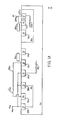
- CMOS device 10 is formed within N-type substrate lla.
- the P-channel device comprises P-type source 13a, P-type drain 17a and gate electrode 16a.
- a P-type channel is induced within N type substrate lla between source 13a and drain 17a upon application of a sufficient negative voltage to gate 16a.
- the N-channel transistor comprises N-type source 19a and N-type drain 21a formed within P-well 18a, and gate electrode 20a.
- the N-channel is induced within P-well 13a between source 19a and drain 21a when a sufficient positive voltage is applied to gate electrode 20a.
- the CMOS device 10 includes N-type substrate contact 12a, which provides electrical connection to substrate lla.
- CMOS device 10 also includes P-type contact 22a, which provides electrical connection to P-well 18a.
- the substrate resistance is shown as resistor 15a
- the P-well resistance is shown as resistor 23a.
- P-type source 13a, N-type substrate lla, and P-well 18a form parasitic PNP transistor 29a.
- N-type substrate lla, P-well 18a, and N-type drain 21a form parasitic NPN transistor 30a.
- the circuit diagram of Figure lb shows an electrical interconnection between the base of PNP transistor 29a and the collector of NPN transistor 30a.
- an electrical interconnection is shown between collector of PNP transistor 29a and the base of NPN transistor 30a because the elements both comprise P-well 18a.
- Substrate resistance 15a (having a resistance value R 1 ) is shown connected between the emitter of PNP transistor 29a (formed by P-type source 13a) and the base of PNP transistor 29a (formed by the substrate lla) because P-type source 13a is connected through substrate contact 12a to substrate resistor 15a.
- NPN transistor 30a the emitter of NPN transistor 30a is shown connected to node 24a, and P-well resistance 23a (having a resistance value of R 2 ) is shown connected between node 24a and the base of NPN transistor 30a, which is the P-well 18a.
- P-well resistance 23a having a resistance value of R 2
- parasitic transistors 29c and 30c are biased off, however, lateral current flow in the substrate lla and P-well 18a can establish potential differences across resistors 15a and 23a which turn on parasitic transistors 29a and 30a.
- node 24a is connected to ground, and terminal 14a is connected to a positive supply voltage (V cc ), typically 5 volts.
- V cc positive supply voltage
- resistor 15a is connected between the emitter 13a and base lla of PNP transistor 29a, base lla is always at a lower potential than emitter 13a.
- PNP transistor 29a turns on, thus applying a positive voltage to base 18a of NPN transistor 30a.
- emitter 2la of transistor 30a With emitter 2la of transistor 30a grounded, transistor 30a turns on, thus drawing current to ground 24a through resistor 15a from the positive supply voltage V cc applied to terminal 14a.
- One prior art method of preventing, or minimizing, the latch-up problem is to provide a very wide field region between the P-channel device and the N-channel device.
- the field region has a minimum width, labelled "d" in Figure la, of 10-15 microns. While use of such a large field region serves to reduce the current gain (Beta) of the parasitic bipolar transistors, thus minimizing current flow through the parasitic transistors, the use of such a large field region also reduces the number of CMOS devices which may be fabricated on a given piece of silicon. Therefore, using large field regions to minimize latch-up results in rather low density devices.
- Rung et al. Another approach to minimize latch-up in CMOS devices is described by Rung et al. in an article entitled "A Retrograde P-well For Higher Density CMOS", IEEE Transactions on Electron Devices, Volume ED-28, No. 10, October 1981, pages 115-119.
- Rung et al. teach that a P-well may be formed to a very shallow depth, thereby minimizing lateral diffusion.
- the Rung P-well utilizes a higher P-type dopant concentration (approximately 2 to 5x10 17 atoms/c2) than prior art P-wells (which utilize a P-well dopant concentration of approximately 2 x10 16 atoms/cm 3 ), thereby minimizing the P-well sheet resistance in order to minimize latch-up.
- increasing the dopant concentration of the P-well increases the capacitance between P-well 18a and N type source 19a, and between P-well 18a and N type drain 21a, thereby decreasing device speed.
- Estreich, et al in an article entitled "An Analysis of Latch-up Prevention in CMOS IC's Using an Epitaxial-Buried Layer Process", IEDM '78 Paper 9.7, December 4-6, 1978, Washington, D.C. and by Payne, et al in an article entitled “Elimination of Latch-up in Bulk CMOS", IEDM '80 Paper 10.2, December 8-10, 1980, Washington, D.C. Estreich, et al and Payne, et al utilize epitaxial silicon formed on a substrate to minimize the sheet resistance of resistor 15a of Figure la.
- Estreich, et al further utilize a buried layer to minimize the resistance of resistor 23a of Figure la.
- the use of epitaxial silicon and buried layers to minimize sheet resistances requires additional processing steps, thus increasing the cost of manufacturing CMOS devices. Furthermore, the requirement of additional processing steps introduces defects, thereby reducing yield.
- This invention prevents latch-up in CMOS devices by preventing conduction of the parasitic transistors.
- this is accomplished by the addition of a voltage drop means comprising one or more diodes between the power supply voltage (V cc ) ' and the positive voltage supply of the CMOS device.
- the voltage drop between the base of the parasitic NPN transistor and ground is increased, thereby further preventing the parasitic NPN transistor from conducting, thus increasing the immunity of CMOS devices constructed in accordance with this invention to latch-up and the problems associated therewith.
- FIG. lc A circuit diagram of one embodiment of this invention is shown in Figure lc.
- the parasitic transistors 29c and 30c are shown as in Figure lb.
- diode 31c in accordance with the teachings of this invention, minimizes latch-up resulting from the presence of the parasitic transistors.
- diode 31c may comprise an NPN transistor having its base and collector connected together.
- 31c may comprise a single PN junction.
- the device power supply voltage V cc (typically 5 volts) is applied to terminal 14c. Because of the presence of diode 31c, the actual voltage supplied to the active devices is equal to V cc minus voltage drop across a forward biased diode (V d ).
- This voltage is available on node 96c. Because of the addition of diode 31c, the voltage drop across resistor 15c must be greater than 2V d (where V d is the voltage drop across a forward-biased PN junction) in order to cause parasitic transistor 29c to turn on. Thus, the power supply voltage V cc must forward bias diode 31c, and the emitter-base junction of parasitic transistor 29c, in order to cause transistor 29c to conduct.
- the substrate resistance 15c (R l ) is sufficiently low (e.g., approximately 1000 ohms) to prevent a voltage drop greater than or equal to 2V d between V cc and the base of parasitic PNP transistor 29c. In this manner, parasitic transistor 29c is prevented from conducting. Because transistor 29c does not conduct, a positive voltage is not applied to the base of transistor 30c, and transistor 30c remains turned off, thus eliminating latch-up.
- FIG. ld A cross sectional view of the circuit of Figure lc is shown in Figure ld. Components similar to the prior art circuits are numbered similarly. However, in accordance with this invention, the structure includes an additional P region 41c forming the base of transistor 31c, contact regions 57c, 58c for contacting P region 41c and N type emitter 51c formed within base 41c.
- the collector of transistor 31c comprises N type substrate llc.
- N diodes connected in series are used in place of diode 31c.
- the resistor 15c must provide a voltage drop greater than (N+1)V d in order to cause transistor 29c to conduct.
- parasitic PNP transistor 29c will not conduct, which in turn prevents the conduction of parasitic NPN transistor 30c, thereby eliminating latch-up.
- a single diode 31c (or set of N diodes connected in series) which is capable of supplying sufficient current to drive the entire integrated circuit device.
- the diode 31c must be capable of supplying 100 milliamps to the integrated circuit.
- a diode 31c capable of ' supplying 100 milliamperes is fabricated in a surface area of only approximately 100 square mils.
- the surface area required to fabricate diode 31c may be reduced.
- P region 41c having a P type dopant concentration of approximately 2x10 18 atoms/cm 3 a diode 31c capable of supplying 100 milliamperes without excessive heat buildup is fabricated in a surface area of approximately 5 square mils.
- This highly doped P region 41c can also be utilized to fabricate additional bipolar transistors having high current carrying ability, for use other than eliminating latch up.
- CMOS device is fabricated having increased latch-up immunity, thereby allowing the field regions of the device to be reduced in width.
- prior art field widths shown in Figure la as distance "d"
- a circuit may be constructed wherein the widths of the field regions between P and N channel devices may be reduced to approximately 0.4 microns.
- the speed of the CMOS circuits constructed in accordance with this invention is increased over prior art CMOS devices utilizing an idential V cc of five volts.
- the gate delay of MOS devices generally decreases with decreasing power supply voltage for small geometry MOS devices.
- P channel devices may be constructed having shorter channel lengths than comparable prior art P channel devices.
- the source 13c is connected to V' cc' which is more negative than the substrate llc connected to V cc .
- the base-emitter junction formed by P channel source 13c and substrate llc is reverse-biased, thereby preventing the conduction of the heretofore undiscussed parasitic PNP transistor formed by P type source 13c (forming the emitter) N type substrate llc (forming the base) and P type drain 17c (forming the collector).
- CMOS devices may be constructed in accordance with this invention having increased performance and increased speed over prior art CMOS devices.
- FIG. le Another embodiment of this invention is shown in schematic diagram of Figure le.
- This embodiment is similar to the embodiment in schematic diagram of Figure lc with the addition of a voltage drop V inserted between the base l8d of NPN parasitic transistor 30d and ground 24d.
- This voltage drop V x tends to reverse-bias the base-emitter junction of parasitic NPN transistor 30d, thus tending to prevent the conduction of NPN transistor 30d.
- a substantially greater current must flow through resistor 23d to ground in order to overcome the voltage V x to forward bias the base-emitter junction of parasitic NPN transistor 30d.
- the insertion of voltage drop V may be used in conjunction with the voltage drop provided by diode 31c, or the voltage drop V may be used alone. In either case, a CMOS device with increased immunity to latch-up is provided, as compared with prior art CMOS devices.
- node 22d is connected to an external "pin" of the semiconductor package containing the CMOS device. Externally to the semiconductor device, a supply voltage V x is connected between the pin connected to node 22d and ground.
- node 22d is connected to an external pin, and one or more PN junctions are connected in series between the pin connected to node 22d (system ground) and node 24d (CMOS device ground). In this manner, a voltage drop V x is provided between base 18d and ground.
- Yet another technique for providing the voltage drop V x between base 18d of the parasitic NPN transistor 30d and ground is to provide a back-bias generator on the semiconductor chip containing the CMOS device.
- a back-bias generator is described by Martino, et al in an article entitled “An On-Dash Chip Back-Bias Generator for MOS Dynamic Memory", IEEE Journal of Solid-State Circuits, Vol. SC-15, No. 5, October 1980, pages 820-825. While the Martino, et al article describes a back-bias generator for use in conjunction with MOS memory devices, this back-bias generator can be used to provide the voltage drop V X on the same silicon chip that contains the remainder of the CMOS device constructed in accordance with this invention.
- the N channel device When the voltage drop V is utilized, the N channel device exhibits the same advantages over prior art N channel devices as does the P channel device of this invention over prior art P channel devices.
- the use of voltage drop V minimizes latch-up problems of CMOS devices, and increases the switching speed of the N channel device, and thus increases the switching speed of the CMOS circuit as a whole constructed in accordance with this invention as compared with prior art CMOS devices due to the decreased power supply voltage applied to the CMOS device.
- CMOS devices are constructed utilizing N channel devices having shorter channel lengths than the N channel devices utilized in prior art CMOS devices, without increased danger of punch-through.
- the current handling ability of the N channel transistor, as well as the speed of the N channel transistor is increased over prior art N channel transistors, thus increasing the current handling ability and speed of the CMOS device constructed in accordance with this invention.
Landscapes
- Engineering & Computer Science (AREA)
- Physics & Mathematics (AREA)
- Microelectronics & Electronic Packaging (AREA)
- Nonlinear Science (AREA)
- Electromagnetism (AREA)
- General Physics & Mathematics (AREA)
- Radar, Positioning & Navigation (AREA)
- Automation & Control Theory (AREA)
- Metal-Oxide And Bipolar Metal-Oxide Semiconductor Integrated Circuits (AREA)
- Semiconductor Integrated Circuits (AREA)
Applications Claiming Priority (2)
| Application Number | Priority Date | Filing Date | Title |
|---|---|---|---|
| US33877882A | 1982-01-11 | 1982-01-11 | |
| US338778 | 1982-01-11 |
Publications (2)
| Publication Number | Publication Date |
|---|---|
| EP0084000A2 true EP0084000A2 (de) | 1983-07-20 |
| EP0084000A3 EP0084000A3 (de) | 1985-07-10 |
Family
ID=23326134
Family Applications (1)
| Application Number | Title | Priority Date | Filing Date |
|---|---|---|---|
| EP83400013A Withdrawn EP0084000A3 (de) | 1982-01-11 | 1983-01-04 | CMOS Anordnung |
Country Status (2)
| Country | Link |
|---|---|
| EP (1) | EP0084000A3 (de) |
| JP (1) | JPS58130557A (de) |
Cited By (7)
| Publication number | Priority date | Publication date | Assignee | Title |
|---|---|---|---|---|
| EP0126184A3 (de) * | 1982-12-23 | 1985-05-15 | Motorola, Inc. | Eingangsschutzschaltung und Vorspannungsverfahren für "scaled" CMOS-Anordnungen |
| GB2158640A (en) * | 1984-04-28 | 1985-11-13 | Mitsubishi Electric Corp | Integrated circuit |
| GB2171249A (en) * | 1985-02-14 | 1986-08-20 | Siliconix Ltd | Improved monolithic integrated circuits |
| DE3507181A1 (de) * | 1985-03-01 | 1986-09-04 | IC - Haus GmbH, 6501 Bodenheim | Schaltungsanordnung zur vermeidung parasitaerer substrat-effekte in integrierten schaltkreisen |
| FR2623016A1 (fr) * | 1987-11-06 | 1989-05-12 | Thomson Semiconducteurs | Dispositif de fusion d'un fusible dans un circuit integre de type cmos |
| WO1989006047A1 (fr) * | 1987-12-23 | 1989-06-29 | Siemens Aktiengesellschaft | Circuit integre a circuit de protection anti-''latch-up'' realise selon la technique des circuits cmos |
| EP0616725A4 (de) * | 1992-10-15 | 1995-03-29 | Standard Microsyst Smc | Elektrische isolation für integrierte schaltungen. |
Families Citing this family (1)
| Publication number | Priority date | Publication date | Assignee | Title |
|---|---|---|---|---|
| JPS648659A (en) * | 1987-06-30 | 1989-01-12 | Mitsubishi Electric Corp | Supplementary semiconductor integrated circuit device |
Family Cites Families (4)
| Publication number | Priority date | Publication date | Assignee | Title |
|---|---|---|---|---|
| US3855549A (en) * | 1973-08-24 | 1974-12-17 | Rca Corp | Circuit, such as cmos crystal oscillator, with reduced power consumption |
| US4039869A (en) * | 1975-11-28 | 1977-08-02 | Rca Corporation | Protection circuit |
| JPS57180159A (en) * | 1981-04-30 | 1982-11-06 | Oki Electric Ind Co Ltd | Mos integrated circuit device |
| JPS5852869A (ja) * | 1981-09-24 | 1983-03-29 | Nec Corp | 半導体装置 |
-
1983
- 1983-01-04 EP EP83400013A patent/EP0084000A3/de not_active Withdrawn
- 1983-01-11 JP JP58001835A patent/JPS58130557A/ja active Pending
Cited By (10)
| Publication number | Priority date | Publication date | Assignee | Title |
|---|---|---|---|---|
| EP0126184A3 (de) * | 1982-12-23 | 1985-05-15 | Motorola, Inc. | Eingangsschutzschaltung und Vorspannungsverfahren für "scaled" CMOS-Anordnungen |
| GB2158640A (en) * | 1984-04-28 | 1985-11-13 | Mitsubishi Electric Corp | Integrated circuit |
| US4772930A (en) * | 1984-04-28 | 1988-09-20 | Mitsubishi Denki Kabushiki Kaisha | Complementary metal oxide semiconductor integrated circuit with unequal reference voltages |
| GB2171249A (en) * | 1985-02-14 | 1986-08-20 | Siliconix Ltd | Improved monolithic integrated circuits |
| DE3507181A1 (de) * | 1985-03-01 | 1986-09-04 | IC - Haus GmbH, 6501 Bodenheim | Schaltungsanordnung zur vermeidung parasitaerer substrat-effekte in integrierten schaltkreisen |
| FR2623016A1 (fr) * | 1987-11-06 | 1989-05-12 | Thomson Semiconducteurs | Dispositif de fusion d'un fusible dans un circuit integre de type cmos |
| EP0320321A1 (de) * | 1987-11-06 | 1989-06-14 | STMicroelectronics S.A. | Anordnung zum Schmelzen einer auf einer integrierten Schaltung aufgebrachten Sicherung |
| WO1989006047A1 (fr) * | 1987-12-23 | 1989-06-29 | Siemens Aktiengesellschaft | Circuit integre a circuit de protection anti-''latch-up'' realise selon la technique des circuits cmos |
| US5126816A (en) * | 1987-12-23 | 1992-06-30 | Siemens Aktiengesellschaft | Integrated circuit with anti latch-up circuit in complementary MOS circuit technology |
| EP0616725A4 (de) * | 1992-10-15 | 1995-03-29 | Standard Microsyst Smc | Elektrische isolation für integrierte schaltungen. |
Also Published As
| Publication number | Publication date |
|---|---|
| JPS58130557A (ja) | 1983-08-04 |
| EP0084000A3 (de) | 1985-07-10 |
Similar Documents
| Publication | Publication Date | Title |
|---|---|---|
| KR950007573B1 (ko) | 회로를 웰로 분리한 반도체장치 | |
| EP0116820B1 (de) | Komplementäre MOS-Schaltung | |
| US4677455A (en) | Semiconductor memory device | |
| US4616243A (en) | Gate protection for a MOSFET | |
| HK1003586B (en) | Semiconductor device | |
| US4491746A (en) | Self-substrate-bias circuit device | |
| KR100243496B1 (ko) | 반도체 장치 | |
| US5721445A (en) | Semiconductor device with increased parasitic emitter resistance and improved latch-up immunity | |
| JP2710113B2 (ja) | 相補性回路技術による集積回路 | |
| US4622573A (en) | CMOS contacting structure having degeneratively doped regions for the prevention of latch-up | |
| US4907059A (en) | Semiconductor bipolar-CMOS inverter | |
| EP0084000A2 (de) | CMOS Anordnung | |
| CA1275457C (en) | Integrated circuit in complementary circuit technology comprising a substrate bias generator | |
| KR100379286B1 (ko) | 보호 회로를 구비한 반도체 장치 | |
| US4812891A (en) | Bipolar lateral pass-transistor for CMOS circuits | |
| KR100613819B1 (ko) | 실리콘 온 인슐레이터 래치 업 펄스 방사선 검출기 | |
| EP0424926A2 (de) | Integrierter Bi-CMOS-Schaltkreis | |
| JP3131525B2 (ja) | Mosパワー・トランジスタ・デバイス | |
| US6320229B1 (en) | Semiconductor device | |
| US6084272A (en) | Electrostatic discharge protective circuit for semiconductor device | |
| US5371023A (en) | Gate circuit, semiconductor integrated circuit device and method of fabrication thereof, semiconductor memory and microprocessor | |
| US6057578A (en) | Protective integrated structure with biasing devices having a predetermined reverse conduction threshold | |
| EP0121096B1 (de) | Halbleiter-Kontaktstruktur | |
| GB2210197A (en) | Latchup and electrostatic discharge protection structure | |
| JP3036905B2 (ja) | 相補型mis半導体装置 |
Legal Events
| Date | Code | Title | Description |
|---|---|---|---|
| PUAI | Public reference made under article 153(3) epc to a published international application that has entered the european phase |
Free format text: ORIGINAL CODE: 0009012 |
|
| AK | Designated contracting states |
Designated state(s): DE FR GB IT NL |
|
| PUAL | Search report despatched |
Free format text: ORIGINAL CODE: 0009013 |
|
| AK | Designated contracting states |
Designated state(s): DE FR GB IT NL |
|
| STAA | Information on the status of an ep patent application or granted ep patent |
Free format text: STATUS: THE APPLICATION IS DEEMED TO BE WITHDRAWN |
|
| 18D | Application deemed to be withdrawn |
Effective date: 19860311 |
|
| RIN1 | Information on inventor provided before grant (corrected) |
Inventor name: CHEN, PETER CHENG-YU |