EP0084178B1 - In einem Halbleitersubstrat ausgeführtes Widerstandselement - Google Patents
In einem Halbleitersubstrat ausgeführtes Widerstandselement Download PDFInfo
- Publication number
- EP0084178B1 EP0084178B1 EP82112097A EP82112097A EP0084178B1 EP 0084178 B1 EP0084178 B1 EP 0084178B1 EP 82112097 A EP82112097 A EP 82112097A EP 82112097 A EP82112097 A EP 82112097A EP 0084178 B1 EP0084178 B1 EP 0084178B1
- Authority
- EP
- European Patent Office
- Prior art keywords
- resistive element
- resistive
- polycrystalline silicon
- impurity
- region
- Prior art date
- Legal status (The legal status is an assumption and is not a legal conclusion. Google has not performed a legal analysis and makes no representation as to the accuracy of the status listed.)
- Expired
Links
Images


Classifications
-
- H—ELECTRICITY
- H10—SEMICONDUCTOR DEVICES; ELECTRIC SOLID-STATE DEVICES NOT OTHERWISE PROVIDED FOR
- H10D—INORGANIC ELECTRIC SEMICONDUCTOR DEVICES
- H10D1/00—Resistors, capacitors or inductors
- H10D1/40—Resistors
- H10D1/43—Resistors having PN junctions
Definitions
- This invention relates to a resistive element formed in a semiconductor substrate.
- a resistive element prepared by diffusing an impurity in a polycrystalline silicon layer is already known.
- This resistive element comprises a low resistive region in which an impurity is diffused and a high resistive region in which no impurity is diffused.
- Figs. 1 and 2 show the conventional resistive element.
- a low resistive region 12 is constructed by diffusing an impurity with, for example, an Si0 2 layer 10 used as a mask.
- a high resistive region 14 has no impurity diffused therein.
- the resistive element should preferably be actuated in a linear region of the V-I curve for the stabilization of its properties. Therefore, the greater the length L-2Xj of the high resistive region, the broader the voltage range in which the resistive element can be linearly operated. Since, however, the mask length L cannot be extended much due to restrictions resulting from a demand for the large scale integration of a semiconductor device, an attempt is made to reduce the length Xj in which an impurity is diffused laterally of a resistive element. This attempt is effected by decreasing the temperature at which an impurity is diffused and applying an impurity having a small diffusion coefficient.
- the lateral diffusion length Xj of an impurity is defined as that which is reached when the impurity is diffused at a concentration of 10 17 cm- 3 , then the lateral diffusion length Xj possible at present measures about 6 microns, making it necessary to further reduce said length Xj.
- a resistive element comprising:
- the resistive element constructed as described above, enables an impurity to be diffused in a smaller length, thereby extending the length of the high resistive region and consequently improving the linear property of a resistive element.
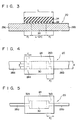
- a thin Si0 2 layer is deposited on the surface of a polycrystalline silicon layer 20.
- a CVD Si0 2 layer for example, is laid on the thin Si0 2 layer.
- the CVD Si0 2 layer and the thin Si0 2 layer are selectively removed by the photoengraving process (PEP) to provide an Si0 2 layer pattern 22 and CVD Si0 2 layer pattern 24.
- the polycrystalline silicon layer 20 comprises the narrow sections 26a and 26b formed by partial etching.
- the Si0 2 layer pattern 22 and CVD Si0 2 layer pattern 24 cover the narrow sections 26a and 26b.
- Phosphorus for example, is diffused in the polycrystalline silicon layer 20 with the Si0 2 layer pattern 24 used as a mask.
- the phosphorus is diffused into the deeper region of the polycrystalline silicon layer 20 through the narrow sections 26a and 26b.
- those portions of the polycrystalline silicon layer 20 in which the phosphorus is diffused constitute low resistive regions 28a and 28b.
- That portion of the polycrystalline silicon layer 20 in which the phosphorus is not diffused constitutes a high resistive region. Since the polycrystalline silicon layer 20 has the narrow sections 26a and 26b, the length Xj of the lateral phosphorus diffusion in the low resistive regions 28a and 28b, as measured from the end of the CVD Si0 2 layer pattern 24, is smaller than in the conventional resistive element.
- the phosphorus impurity is more broadly spread at a smaller concentration after passing through the narrow sections 26a and 26b. If the narrow sections 26a and 26b are designed to have a low resistance, then the property of the resistive element is not adversely affected, even though the polycrystalline silicon layer 20 is made narrower in some parts.
- the length L-2Xj of the high resistive region 30 can be extended, thereby broadening the voltage range in which a resistive element can be applied in the linear region.
- the width x of the high resistive region 30 is 10 microns; the length y of the narrow sections 26a and 26b is 2 microns; and the width z of the narrow sections 26a and 26b is 1 micron.
- the diffusion length Xj of the impurity is made about 2 microns shorter than has been possible with the conventional resistive element as measured on the basis of the same manufacturing process.
- a polycrystalline silicon layer 20 comprises a high resistive region 30 and narrow low resistive regions 28a and 28b. Only the junctions defined by the high resistive region 30 with the narrow low resistive regions 28a and 28b are made wide.
- An impurity is diffused in the wide polycrystalline silicon layer portion 20 at the narrow sections 28a and 28b through a mask 24 formed on the polycrystalline silicon layer 20, thereby constituting the low resistive regions 28a and 28b. In this case, too, the impurity is widely spread at a lower concentration after passing through the narrow sections 32a and 32b. With the modification of Fig. 5, therefore, the lateral diffusion length Xj of the impurity is also made shorter than in the conventional resistive element.
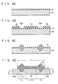
- Fig. 6D is a cross sectional view of the second embodiment.
- Figs. 6A through 6D show the sequential steps of manufacturing this embodiment.
- a polycrystalline silicon layer 20 is patterned, and later the surface of the layer 20 is oxidized to produce an Si0 2 layer 21.
- a silicon nitride layer deposited on the Si0 2 layer 21 is etched by the photoengraving process to produce silicon nitride patterns 36 and holes 38a and 38b (Fig. 6B).
- the polycrystalline silicon layer 20 is selectively oxidized through the masks of the silicon nitride patterns 36 (Fig. 6C). During this oxidizing process, those portions of the polycrystalline silicon layer 20 which lie underthe holes 38a and 38b are made thinner. Later, as shown in Fig.
- a CVD Si0 2 layer formed by the CVD process is selectively etched to provide an Si0 2 pattern 40 having a length L and CVD Si0 2 pattern 42.
- Phosphorus for example, is diffused in the resistive layerthrough the masks of said Si0 2 pattern 40 and CVD Si0 2 pattern 42, thereby forming low resistive regions 44a and 44b in which the phosphorus is laterally diffused in a length Xj.
- Those portions of the polycrystalline silicon layer 20 in which no phosphorus is diffused constitutes a high resistive region having a length L-2Xj.
- the path through which the impurity is diffused has narrower portions.
- the impurity is widely spread at a lower concentration, thereby shortening the lateral diffusion length Xj of the impurity.
- X measures 0.6 micron; Y 2 microns; and Z 0.06 micron.
- the second embodiment of Figs. 6A through 6D enables the lateral diffusion length Xj of the impurity to be made about 2 microns shorter than has been possible with the conventional resistive element, thereby improving the linear property of the resistive element.
- a mask 50 prepared from, for example, Si0 2 or Si 3 N 4 is selectively formed on a polycrystalline silicon layer 20 (Fig. 7A). Another polycrystalline silicon layer is deposited on the polycrystalline silicon layer through the mask 50 (Fig. 7B). A CVD Si0 2 layerformed by the CVD process is selectively etched to produce a CVD Si0 2 pattern 52 (Fig. 7C). Phosphorus, for example, is diffused with the CVD Si0 2 pattern as a mask to provide low resistive regions 54a and 54b and a high resistive region 56. An impurity is laterally diffused over a short length of a resistive element produced through the above-mentioned steps, which, therefore, indicates an excellent linear property.
Landscapes
- Semiconductor Integrated Circuits (AREA)
Claims (4)
Applications Claiming Priority (4)
| Application Number | Priority Date | Filing Date | Title |
|---|---|---|---|
| JP4711/82 | 1982-01-14 | ||
| JP57004713A JPS58122768A (ja) | 1982-01-14 | 1982-01-14 | 半導体装置 |
| JP4713/82 | 1982-01-14 | ||
| JP57004711A JPS58122767A (ja) | 1982-01-14 | 1982-01-14 | 半導体装置 |
Publications (3)
| Publication Number | Publication Date |
|---|---|
| EP0084178A2 EP0084178A2 (de) | 1983-07-27 |
| EP0084178A3 EP0084178A3 (en) | 1985-05-22 |
| EP0084178B1 true EP0084178B1 (de) | 1988-06-08 |
Family
ID=26338528
Family Applications (1)
| Application Number | Title | Priority Date | Filing Date |
|---|---|---|---|
| EP82112097A Expired EP0084178B1 (de) | 1982-01-14 | 1982-12-29 | In einem Halbleitersubstrat ausgeführtes Widerstandselement |
Country Status (3)
| Country | Link |
|---|---|
| US (1) | US4455547A (de) |
| EP (1) | EP0084178B1 (de) |
| DE (1) | DE3278654D1 (de) |
Families Citing this family (4)
| Publication number | Priority date | Publication date | Assignee | Title |
|---|---|---|---|---|
| GB8710359D0 (en) * | 1987-05-01 | 1987-06-03 | Inmos Ltd | Semiconductor element |
| US5236857A (en) * | 1991-10-30 | 1993-08-17 | Texas Instruments Incorporated | Resistor structure and process |
| US6529152B1 (en) | 1999-10-15 | 2003-03-04 | Cyngal Integrated Products, Inc. | High precision SAR converter using resistor strip with auto zeroing function |
| US6532568B1 (en) * | 2000-10-30 | 2003-03-11 | Delphi Technologies, Inc. | Apparatus and method for conditioning polysilicon circuit elements |
Family Cites Families (4)
| Publication number | Priority date | Publication date | Assignee | Title |
|---|---|---|---|---|
| US4124933A (en) * | 1974-05-21 | 1978-11-14 | U.S. Philips Corporation | Methods of manufacturing semiconductor devices |
| US4197632A (en) * | 1975-12-05 | 1980-04-15 | Nippon Electric Co., Ltd. | Semiconductor device |
| JPS5351985A (en) * | 1976-10-22 | 1978-05-11 | Hitachi Ltd | Semiconductor wiring constitution |
| IT1094517B (it) * | 1978-04-28 | 1985-08-02 | Componenti Elettronici Sgs Ate | Procedimento per la fabbricazione di un elemento resistivo filiforme per circuito integrato |
-
1982
- 1982-12-29 DE DE8282112097T patent/DE3278654D1/de not_active Expired
- 1982-12-29 EP EP82112097A patent/EP0084178B1/de not_active Expired
-
1983
- 1983-01-05 US US06/455,837 patent/US4455547A/en not_active Expired - Lifetime
Also Published As
| Publication number | Publication date |
|---|---|
| EP0084178A3 (en) | 1985-05-22 |
| DE3278654D1 (en) | 1988-07-14 |
| EP0084178A2 (de) | 1983-07-27 |
| US4455547A (en) | 1984-06-19 |
Similar Documents
| Publication | Publication Date | Title |
|---|---|---|
| US4551743A (en) | Semiconductor integrated circuit with isolation region made of dielectric material | |
| US5567977A (en) | Precision integrated resistor | |
| KR100973866B1 (ko) | 반도체 장치 및 반도체 장치 제조방법 | |
| EP0100166B1 (de) | Halbleiteranordnung mit einer Verbindungsstruktur | |
| US5759887A (en) | Semiconductor device and a method of manufacturing a semiconductor device | |
| EP0084178B1 (de) | In einem Halbleitersubstrat ausgeführtes Widerstandselement | |
| US4551906A (en) | Method for making self-aligned lateral bipolar transistors | |
| NL9202131A (nl) | Halfgeleiderinrichting en werkwijze voor het maken daarvan. | |
| US5304838A (en) | Vertical resistive element for integrated circuit miniaturization | |
| KR100313412B1 (ko) | 집적회로용저항기의형성방법 | |
| US5314836A (en) | Method of making a single electrode level CCD | |
| JPH06204408A (ja) | 半導体装置用拡散抵抗 | |
| US20040235258A1 (en) | Method of forming resistive structures | |
| JPH08172135A (ja) | 半導体装置の製造方法および半導体集積回路装置 | |
| EP0279902A2 (de) | Verfahren zur Herstellung einer Hochspannungshalbleiteranordnung | |
| US3853644A (en) | Transistor for super-high frequency and method of manufacturing it | |
| EP1017092A1 (de) | Herstellung eines in einer integrierten Schaltung verwendeten Widerstands | |
| JPH01192159A (ja) | 半導体装置 | |
| US3895978A (en) | Method of manufacturing transistors | |
| US6087675A (en) | Semiconductor device with an insulation film having emitter contact windows filled with polysilicon film | |
| JPH0997876A (ja) | 半導体装置及びその製造方法 | |
| RU1144570C (ru) | Поликремниевый резистор и способ его изготовлени | |
| JPS5934999Y2 (ja) | 抵抗体 | |
| KR950011565B1 (ko) | 반도체 장치의 제조방법 | |
| KR920010135B1 (ko) | 고저항기 제조 방법 |
Legal Events
| Date | Code | Title | Description |
|---|---|---|---|
| PUAI | Public reference made under article 153(3) epc to a published international application that has entered the european phase |
Free format text: ORIGINAL CODE: 0009012 |
|
| 17P | Request for examination filed |
Effective date: 19821229 |
|
| AK | Designated contracting states |
Designated state(s): DE FR GB |
|
| RAP1 | Party data changed (applicant data changed or rights of an application transferred) |
Owner name: KABUSHIKI KAISHA TOSHIBA |
|
| PUAL | Search report despatched |
Free format text: ORIGINAL CODE: 0009013 |
|
| AK | Designated contracting states |
Designated state(s): DE FR GB |
|
| 17Q | First examination report despatched |
Effective date: 19860825 |
|
| GRAA | (expected) grant |
Free format text: ORIGINAL CODE: 0009210 |
|
| AK | Designated contracting states |
Kind code of ref document: B1 Designated state(s): DE FR GB |
|
| REF | Corresponds to: |
Ref document number: 3278654 Country of ref document: DE Date of ref document: 19880714 |
|
| ET | Fr: translation filed | ||
| PLBE | No opposition filed within time limit |
Free format text: ORIGINAL CODE: 0009261 |
|
| STAA | Information on the status of an ep patent application or granted ep patent |
Free format text: STATUS: NO OPPOSITION FILED WITHIN TIME LIMIT |
|
| 26N | No opposition filed | ||
| PGFP | Annual fee paid to national office [announced via postgrant information from national office to epo] |
Ref country code: FR Payment date: 19961211 Year of fee payment: 15 |
|
| PGFP | Annual fee paid to national office [announced via postgrant information from national office to epo] |
Ref country code: GB Payment date: 19961220 Year of fee payment: 15 |
|
| PGFP | Annual fee paid to national office [announced via postgrant information from national office to epo] |
Ref country code: DE Payment date: 19970107 Year of fee payment: 15 |
|
| PG25 | Lapsed in a contracting state [announced via postgrant information from national office to epo] |
Ref country code: GB Free format text: LAPSE BECAUSE OF NON-PAYMENT OF DUE FEES Effective date: 19971229 |
|
| PG25 | Lapsed in a contracting state [announced via postgrant information from national office to epo] |
Ref country code: FR Free format text: THE PATENT HAS BEEN ANNULLED BY A DECISION OF A NATIONAL AUTHORITY Effective date: 19971231 |
|
| GBPC | Gb: european patent ceased through non-payment of renewal fee |
Effective date: 19971229 |
|
| PG25 | Lapsed in a contracting state [announced via postgrant information from national office to epo] |
Ref country code: DE Free format text: LAPSE BECAUSE OF NON-PAYMENT OF DUE FEES Effective date: 19980901 |
|
| REG | Reference to a national code |
Ref country code: FR Ref legal event code: ST |