EP0084424A2 - Chemische Entfernung von ausgelaufenem Harz von verkapselten Anordnungen und gemäss diesem Verfahren behandelte Anordung - Google Patents
Chemische Entfernung von ausgelaufenem Harz von verkapselten Anordnungen und gemäss diesem Verfahren behandelte Anordung Download PDFInfo
- Publication number
- EP0084424A2 EP0084424A2 EP83300119A EP83300119A EP0084424A2 EP 0084424 A2 EP0084424 A2 EP 0084424A2 EP 83300119 A EP83300119 A EP 83300119A EP 83300119 A EP83300119 A EP 83300119A EP 0084424 A2 EP0084424 A2 EP 0084424A2
- Authority
- EP
- European Patent Office
- Prior art keywords
- solvent
- resin
- resin bleed
- bleed
- encapsulated
- Prior art date
- Legal status (The legal status is an assumption and is not a legal conclusion. Google has not performed a legal analysis and makes no representation as to the accuracy of the status listed.)
- Withdrawn
Links
Images

Classifications
-
- H—ELECTRICITY
- H10—SEMICONDUCTOR DEVICES; ELECTRIC SOLID-STATE DEVICES NOT OTHERWISE PROVIDED FOR
- H10W—GENERIC PACKAGES, INTERCONNECTIONS, CONNECTORS OR OTHER CONSTRUCTIONAL DETAILS OF DEVICES COVERED BY CLASS H10
- H10W74/00—Encapsulations, e.g. protective coatings
- H10W74/01—Manufacture or treatment
-
- H—ELECTRICITY
- H10—SEMICONDUCTOR DEVICES; ELECTRIC SOLID-STATE DEVICES NOT OTHERWISE PROVIDED FOR
- H10W—GENERIC PACKAGES, INTERCONNECTIONS, CONNECTORS OR OTHER CONSTRUCTIONAL DETAILS OF DEVICES COVERED BY CLASS H10
- H10W70/00—Package substrates; Interposers; Redistribution layers [RDL]
- H10W70/01—Manufacture or treatment
- H10W70/04—Manufacture or treatment of leadframes
- H10W70/045—Cleaning
-
- H—ELECTRICITY
- H10—SEMICONDUCTOR DEVICES; ELECTRIC SOLID-STATE DEVICES NOT OTHERWISE PROVIDED FOR
- H10W—GENERIC PACKAGES, INTERCONNECTIONS, CONNECTORS OR OTHER CONSTRUCTIONAL DETAILS OF DEVICES COVERED BY CLASS H10
- H10W72/00—Interconnections or connectors in packages
- H10W72/50—Bond wires
- H10W72/541—Dispositions of bond wires
- H10W72/5449—Dispositions of bond wires not being orthogonal to a side surface of the chip, e.g. fan-out arrangements
-
- H—ELECTRICITY
- H10—SEMICONDUCTOR DEVICES; ELECTRIC SOLID-STATE DEVICES NOT OTHERWISE PROVIDED FOR
- H10W—GENERIC PACKAGES, INTERCONNECTIONS, CONNECTORS OR OTHER CONSTRUCTIONAL DETAILS OF DEVICES COVERED BY CLASS H10
- H10W90/00—Package configurations
- H10W90/701—Package configurations characterised by the relative positions of pads or connectors relative to package parts
- H10W90/751—Package configurations characterised by the relative positions of pads or connectors relative to package parts of bond wires
- H10W90/756—Package configurations characterised by the relative positions of pads or connectors relative to package parts of bond wires between a chip and a stacked lead frame, conducting package substrate or heat sink
Definitions
- Plastic material used for forming such a moulded package typically comprises epoxy silicone or epoxy novalac, for example any of the following materials, namely the material designated Dow Corning 631, available from Dow Corning, the materials designated Plaskon 3200LS and Plaskon 292B available from Plaskon Corporation of Toledo, Ohio, the materials designated Hysol MH 19F-0294 and Hysol MH 20F available from Hysol Corporation, Olean, New York, or the materials designated Morton 410B and Morton 421, available from Morton Corporation of Woodstock, Illinois. Other plastics materials may, of course, be used.
- Epoxy silicone is described, for example, in United States Patent No. 4,202,811.
- the lead frame is placed in the lower half of a two-piece mould.
- the upper half of the mould is then brought into contact with the lower half, so that the lead frame is located between the two halves of the mould with the leads extending out of the mould cavity.
- Those portions of the lead frame which are to be encapsulated are located within the mould during the encapsulation process.
- This small amount of encapsulating material often called "resin bleed" typically comprises the same material as that used to encapsulate the semiconductor die.
- a method for the chemical removal of resin bleed from an encapsulated semiconductor device characterized by the step of applying to said encapsulated device a material which is a solvent of the resin for a time sufficient to remove said resin bleed, but for a time insufficient to cause appreciable damage to the device encapsulation.
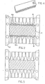
- FIG. 2 shows the device, including the peripheral portion of the lead frame, referenced 10, after the semiconductor die and the central portion of the lead frame have been encapsulated in a body 11 of synthetic resin. Resin bleed, indicated at 12a, 12b, is shown as extending from the body 11 over the lead 15. The moulded parts of the package are first deflashed, the encapsulating material being removed from between adjacent leads at the same time as those portions of the lead frame holding the leads fixed during the moulding operation are removed.
- the encapsulated device is next cleaned, for example, by dipping in a 50% sulfuric acid solution at approximately 85 0 C, followed by a rinse in de-ionized water.
- This cleaning step serves to slightly etch the lead frame material under the resin bleed which aids in the removal of the resin bleed.
- this cleaning step is not essential to the removal of resin bleed in accordance with this invention.
- the resin bleed 12a, 12b of Figure 2 is then removed by applying to the encapsulated device a chemical which is capable of acting as a solvent with respect to the resin bleed material.
- a solvent may comprise, for example, a haloginated hydrocarbon, an organic acid and a haloginated hydrocarbon, an inorganic acid and a haloginated hydrocarbon, or a base and a haloginated hydrocarbon.
- haloginated hydrocarbons include chlorinated hydrocarbons, such as methylene chloride, for example.
- Other compounds can be used in place of methylene chloride, such as cyclic amides (for example, N-methyl-2-pyrrolidene) and oxyginated sulfers (for example, dimethyl sulfoxide).
- Organic acids which are suitable include formic acid, phenol (carbolic acid), and carboxylic acids, such as acetic acid, for example.
- One such commercially available solvent is Dynasolve 160, manufactured and sold by Dynaloy, Inc. of Hanover, New Jersey. Dynasolve comprises a mixture of methylene chloride, phenol, acetic acid, and formic acid. Prior to the discovery that such solvents can be utilized to remove resin bleed after encapsulation, such solvents were used for the removal of substantially all of the encapsulating material surrounding the semi- conductor die for the purpose of detailed visual, electrical and mechanical analysis of the semiconductor die and bonding wires connected between the semiconductor die and the lead frame.
- the encapsulated device is preferably submerged in the solvent, for example in a tank, and ultrasonic energy applied to the solvent to agitate it during the time that the device is submerged.
- ultrasonic energy applied to the solvent to agitate it during the time that the device is submerged.
- other means for agitating the solvent is used.
- Dynasolve 160 When Dynasolve 160 is utilized as a solvent for the removal of resin bleed, Dynasolve 160 may be utilized at either room temperature or higher temperatures, up to the boiling point of Dynasolve 160 (approximately 40 o C), and in general at a temperature between 20°C and 40°C. When devices are submerged in Dynasolve 160 at room temperature which is agitated by ultrasonic energy, approximately 15 to 20 minutes is required to remove all traces of resin bleed. Similarly, when devices are submerged in Dynasolve 160 which is heated to approximately 35°C and agitated by ultrasonic energy, approximately 15 minutes is required to remove all traces of resin bleed.
- an evaporation seal is formed on top of the solvent in the tank.
- water or other suitable liquids or materials, can be used to form an evaporation seal on the surface to a thickness, for example, within the range of approximately 3/4 to 1 inch, although this thickness is not critical. This is easily done, because the density of water is sufficiently less than the density of the solvent to allow the formation of the water seal, even when ultrasonic energy or other means are used to agitate the solvent.
- Evaporation of the solvent is further minimized by utilizing a cooling coil of well known design near the top of the tank containing the solvent, thereby causing the condensation of substantially all vaporized solvent.
- Uresolve-R and Uresolve-S.G. are typically utilized at room temperature for approximately 30 minutes in order to remove all traces of resin bleed.
- Uresolve-R or Uresolve-S.G. are heated to a temperature in excess of approximately 90°C t 5°C, undesirable discolouration of the package body will result, although the colour of the package body is not critical to the mechanical or electrical quality or reliability of an encapsulated semiconductor device.
- the above times and temperatures are based upon the application of ultrasonic energy to the solvent (i.e. approximately 400-1300 watts at approximately 25 KHz applied to a 10 to 15 U.S. gallon (37850 to 56775 CC) volume of solvent) during the removal of resin bleed from an encapsulated device in accordance with the teachings of this invention.
- the application of ultrasonic energy is accomplished, for example, by utilizing the Branson model EML 70-36 ultrasonic generator available from Branson Cleaning Equipment Company of Shelton, Connecticut.
- the size of the devices being cleaned is inversely proportional to the number of devices which can be completely by cleaned of all resin bleed in a single cleaning cycle. For example, utilizing a 15 U.S. gallon volume of Dynasolve 160 with a water seal and cooling coils, as previously described, and approximately 1260 watts of 25 KHz ultrasonic energy, thereby removing all traces of resin bleed, following cycle times and quantities are achieved:
- the device After removal of the resin bleed from the device, the device is rinsed. With the resin bleed removed, the lead frame is plated or solder-dipped in known fashion.
Landscapes
- Encapsulation Of And Coatings For Semiconductor Or Solid State Devices (AREA)
Applications Claiming Priority (4)
| Application Number | Priority Date | Filing Date | Title |
|---|---|---|---|
| US33789682A | 1982-01-07 | 1982-01-07 | |
| US337896 | 1982-01-07 | ||
| US45130882A | 1982-12-22 | 1982-12-22 | |
| US451308 | 1982-12-22 |
Publications (2)
| Publication Number | Publication Date |
|---|---|
| EP0084424A2 true EP0084424A2 (de) | 1983-07-27 |
| EP0084424A3 EP0084424A3 (de) | 1984-06-13 |
Family
ID=26990916
Family Applications (1)
| Application Number | Title | Priority Date | Filing Date |
|---|---|---|---|
| EP83300119A Withdrawn EP0084424A3 (de) | 1982-01-07 | 1983-01-07 | Chemische Entfernung von ausgelaufenem Harz von verkapselten Anordnungen und gemäss diesem Verfahren behandelte Anordung |
Country Status (2)
| Country | Link |
|---|---|
| EP (1) | EP0084424A3 (de) |
| KR (1) | KR840003533A (de) |
Cited By (5)
| Publication number | Priority date | Publication date | Assignee | Title |
|---|---|---|---|---|
| DE3446647A1 (de) * | 1984-02-22 | 1985-08-29 | Kabushiki Kaisha Toshiba, Kawasaki, Kanagawa | Verfahren zur herstellung von kunstharzversiegelten halbleitervorrichtungen |
| WO1986007492A1 (en) * | 1985-06-11 | 1986-12-18 | American Telephone & Telegraph Company | Lead frame deflashing |
| EP0354800A3 (de) * | 1988-08-12 | 1990-12-27 | Mitsui Petrochemical Industries, Ltd. | Verfahren zum Herstellen von Halbleiteranordnungen |
| EP0789507A3 (de) * | 1996-02-08 | 1998-02-25 | Bayerische Motoren Werke Aktiengesellschaft, Patentabteilung AJ-3 | Eingekapseltes elektronisches Steuergerät und Verfahren zu seiner Herstellung |
| CN109187537A (zh) * | 2018-08-17 | 2019-01-11 | 新华三技术有限公司 | 元器件封胶溶解液以及元器件的开封方法和失效分析方法 |
Family Cites Families (2)
| Publication number | Priority date | Publication date | Assignee | Title |
|---|---|---|---|---|
| DE2930760A1 (de) * | 1979-07-28 | 1981-02-12 | Itt Ind Gmbh Deutsche | Verfahren zum umhuellen von halbleiterbauelementen mittels spritzgiessens |
| JPS5694636A (en) * | 1979-12-27 | 1981-07-31 | Hitachi Ltd | Manufacture of semiconductor device sealed by resin |
-
1983
- 1983-01-07 KR KR1019830000046A patent/KR840003533A/ko not_active Ceased
- 1983-01-07 EP EP83300119A patent/EP0084424A3/de not_active Withdrawn
Cited By (6)
| Publication number | Priority date | Publication date | Assignee | Title |
|---|---|---|---|---|
| DE3446647A1 (de) * | 1984-02-22 | 1985-08-29 | Kabushiki Kaisha Toshiba, Kawasaki, Kanagawa | Verfahren zur herstellung von kunstharzversiegelten halbleitervorrichtungen |
| WO1986007492A1 (en) * | 1985-06-11 | 1986-12-18 | American Telephone & Telegraph Company | Lead frame deflashing |
| EP0354800A3 (de) * | 1988-08-12 | 1990-12-27 | Mitsui Petrochemical Industries, Ltd. | Verfahren zum Herstellen von Halbleiteranordnungen |
| US5070041A (en) * | 1988-08-12 | 1991-12-03 | Mitsui Petrochemical Industries, Ltd. | Method of removing flash from a semiconductor leadframe using coated leadframe and solvent |
| EP0789507A3 (de) * | 1996-02-08 | 1998-02-25 | Bayerische Motoren Werke Aktiengesellschaft, Patentabteilung AJ-3 | Eingekapseltes elektronisches Steuergerät und Verfahren zu seiner Herstellung |
| CN109187537A (zh) * | 2018-08-17 | 2019-01-11 | 新华三技术有限公司 | 元器件封胶溶解液以及元器件的开封方法和失效分析方法 |
Also Published As
| Publication number | Publication date |
|---|---|
| EP0084424A3 (de) | 1984-06-13 |
| KR840003533A (ko) | 1984-09-08 |
Similar Documents
| Publication | Publication Date | Title |
|---|---|---|
| US6230719B1 (en) | Apparatus for removing contaminants on electronic devices | |
| JP4669019B2 (ja) | 基板ホルダ及び電解めっき装置 | |
| JP3827627B2 (ja) | めっき装置及びめっき方法 | |
| US20050016565A1 (en) | Cleaning masks | |
| GB2195826A (en) | A lead frame for a semiconductor device | |
| EP0084424A2 (de) | Chemische Entfernung von ausgelaufenem Harz von verkapselten Anordnungen und gemäss diesem Verfahren behandelte Anordung | |
| JP2023509239A (ja) | 導電性膜を備えた側壁メッキ用パッケージ方法 | |
| US2857560A (en) | Semiconductor unit and method of making it | |
| WO1995003624A1 (en) | Coated bonding wires in high lead count packages | |
| US5215593A (en) | Method of introducing liquid into small-diameter hole | |
| CN116705621A (zh) | 一种引线框架及其制备方法 | |
| US5336564A (en) | Miniature keeper bar | |
| TW434846B (en) | Mold die for semiconductor package | |
| US3876461A (en) | Semiconductor process | |
| JPS58140133A (ja) | プラスチツク半導体パツケ−ジリ−ド上の樹脂のブリ−ドの化学的除去 | |
| JPH03502855A (ja) | 半導体装置、その製造方法、その方法を実行するための装置、および組立装置 | |
| US20200402900A1 (en) | Method of manufacturing semiconductor devices and corresponding semiconductor device | |
| WO2005010947A2 (en) | Cleaning masks | |
| JPH0496238A (ja) | 半導体装置の製造方法 | |
| SE452660B (sv) | Metod for att preparera prov for undersokning av kvaliteten pa metallbeleggningar i hal i ett monsterkort | |
| KR200345152Y1 (ko) | 바렐을 이용한 반도체 패키지 소자의 전해 디플래쉬 장치 | |
| KR100572896B1 (ko) | 바렐을 이용한 반도체 패키지 소자의 전해 디플래쉬 장치및 그 방법 | |
| JPS572536A (en) | Semiconductor device | |
| CN117210226A (zh) | 腐蚀液、开封方法 | |
| EP0496078A1 (de) | Form zur Herstellung von Kunststoffpackungen für integrierte Schaltungen, die eine Wärmesenke enthalten |
Legal Events
| Date | Code | Title | Description |
|---|---|---|---|
| PUAI | Public reference made under article 153(3) epc to a published international application that has entered the european phase |
Free format text: ORIGINAL CODE: 0009012 |
|
| AK | Designated contracting states |
Designated state(s): DE FR GB IT NL SE |
|
| EL | Fr: translation of claims filed | ||
| TCNL | Nl: translation of patent claims filed | ||
| PUAL | Search report despatched |
Free format text: ORIGINAL CODE: 0009013 |
|
| AK | Designated contracting states |
Designated state(s): DE FR GB IT NL SE |
|
| STAA | Information on the status of an ep patent application or granted ep patent |
Free format text: STATUS: THE APPLICATION IS DEEMED TO BE WITHDRAWN |
|
| 18D | Application deemed to be withdrawn |
Effective date: 19850214 |
|
| RIN1 | Information on inventor provided before grant (corrected) |
Inventor name: LEE, JONG-SANG |