EP0084465A2 - Oxyd-isolierungsverfahren für Standard RAM/PROM und laterale PNP Zelle RAM - Google Patents
Oxyd-isolierungsverfahren für Standard RAM/PROM und laterale PNP Zelle RAM Download PDFInfo
- Publication number
- EP0084465A2 EP0084465A2 EP83400012A EP83400012A EP0084465A2 EP 0084465 A2 EP0084465 A2 EP 0084465A2 EP 83400012 A EP83400012 A EP 83400012A EP 83400012 A EP83400012 A EP 83400012A EP 0084465 A2 EP0084465 A2 EP 0084465A2
- Authority
- EP
- European Patent Office
- Prior art keywords
- region
- regions
- epitaxial layer
- conductivity type
- islands
- Prior art date
- Legal status (The legal status is an assumption and is not a legal conclusion. Google has not performed a legal analysis and makes no representation as to the accuracy of the status listed.)
- Granted
Links
Images



Classifications
-
- H—ELECTRICITY
- H10—SEMICONDUCTOR DEVICES; ELECTRIC SOLID-STATE DEVICES NOT OTHERWISE PROVIDED FOR
- H10D—INORGANIC ELECTRIC SEMICONDUCTOR DEVICES
- H10D84/00—Integrated devices formed in or on semiconductor substrates that comprise only semiconducting layers, e.g. on Si wafers or on GaAs-on-Si wafers
- H10D84/01—Manufacture or treatment
- H10D84/0112—Integrating together multiple components covered by H10D8/00, H10D10/00 or H10D18/00, e.g. integrating multiple BJTs
- H10D84/0114—Integrating together multiple components covered by H10D8/00, H10D10/00 or H10D18/00, e.g. integrating multiple BJTs the components including vertical BJTs and lateral BJTs
-
- H—ELECTRICITY
- H10—SEMICONDUCTOR DEVICES; ELECTRIC SOLID-STATE DEVICES NOT OTHERWISE PROVIDED FOR
- H10B—ELECTRONIC MEMORY DEVICES
- H10B69/00—Erasable-and-programmable ROM [EPROM] devices not provided for in groups H10B41/00 - H10B63/00, e.g. ultraviolet erasable-and-programmable ROM [UVEPROM] devices
-
- H—ELECTRICITY
- H10—SEMICONDUCTOR DEVICES; ELECTRIC SOLID-STATE DEVICES NOT OTHERWISE PROVIDED FOR
- H10D—INORGANIC ELECTRIC SEMICONDUCTOR DEVICES
- H10D62/00—Semiconductor bodies, or regions thereof, of devices having potential barriers
- H10D62/10—Shapes, relative sizes or dispositions of the regions of the semiconductor bodies; Shapes of the semiconductor bodies
- H10D62/102—Constructional design considerations for preventing surface leakage or controlling electric field concentration
- H10D62/103—Constructional design considerations for preventing surface leakage or controlling electric field concentration for increasing or controlling the breakdown voltage of reverse-biased devices
- H10D62/105—Constructional design considerations for preventing surface leakage or controlling electric field concentration for increasing or controlling the breakdown voltage of reverse-biased devices by having particular doping profiles, shapes or arrangements of PN junctions; by having supplementary regions, e.g. junction termination extension [JTE]
-
- H—ELECTRICITY
- H10—SEMICONDUCTOR DEVICES; ELECTRIC SOLID-STATE DEVICES NOT OTHERWISE PROVIDED FOR
- H10D—INORGANIC ELECTRIC SEMICONDUCTOR DEVICES
- H10D84/00—Integrated devices formed in or on semiconductor substrates that comprise only semiconducting layers, e.g. on Si wafers or on GaAs-on-Si wafers
- H10D84/01—Manufacture or treatment
- H10D84/02—Manufacture or treatment characterised by using material-based technologies
- H10D84/03—Manufacture or treatment characterised by using material-based technologies using Group IV technology, e.g. silicon technology or silicon-carbide [SiC] technology
- H10D84/038—Manufacture or treatment characterised by using material-based technologies using Group IV technology, e.g. silicon technology or silicon-carbide [SiC] technology using silicon technology, e.g. SiGe
-
- H—ELECTRICITY
- H10—SEMICONDUCTOR DEVICES; ELECTRIC SOLID-STATE DEVICES NOT OTHERWISE PROVIDED FOR
- H10D—INORGANIC ELECTRIC SEMICONDUCTOR DEVICES
- H10D84/00—Integrated devices formed in or on semiconductor substrates that comprise only semiconducting layers, e.g. on Si wafers or on GaAs-on-Si wafers
- H10D84/60—Integrated devices formed in or on semiconductor substrates that comprise only semiconducting layers, e.g. on Si wafers or on GaAs-on-Si wafers characterised by the integration of at least one component covered by groups H10D10/00 or H10D18/00, e.g. integration of BJTs
- H10D84/65—Integrated injection logic
-
- H—ELECTRICITY
- H10—SEMICONDUCTOR DEVICES; ELECTRIC SOLID-STATE DEVICES NOT OTHERWISE PROVIDED FOR
- H10W—GENERIC PACKAGES, INTERCONNECTIONS, CONNECTORS OR OTHER CONSTRUCTIONAL DETAILS OF DEVICES COVERED BY CLASS H10
- H10W10/00—Isolation regions in semiconductor bodies between components of integrated devices
- H10W10/01—Manufacture or treatment
- H10W10/011—Manufacture or treatment of isolation regions comprising dielectric materials
- H10W10/012—Manufacture or treatment of isolation regions comprising dielectric materials using local oxidation of silicon [LOCOS]
- H10W10/0121—Manufacture or treatment of isolation regions comprising dielectric materials using local oxidation of silicon [LOCOS] in regions recessed from the surface, e.g. in trenches or grooves
- H10W10/0124—Manufacture or treatment of isolation regions comprising dielectric materials using local oxidation of silicon [LOCOS] in regions recessed from the surface, e.g. in trenches or grooves the regions having non-rectangular shapes, e.g. rounded
-
- H—ELECTRICITY
- H10—SEMICONDUCTOR DEVICES; ELECTRIC SOLID-STATE DEVICES NOT OTHERWISE PROVIDED FOR
- H10W—GENERIC PACKAGES, INTERCONNECTIONS, CONNECTORS OR OTHER CONSTRUCTIONAL DETAILS OF DEVICES COVERED BY CLASS H10
- H10W10/00—Isolation regions in semiconductor bodies between components of integrated devices
- H10W10/10—Isolation regions comprising dielectric materials
- H10W10/13—Isolation regions comprising dielectric materials formed using local oxidation of silicon [LOCOS], e.g. sealed interface localised oxidation [SILO] or side-wall mask isolation [SWAMI]
Definitions
- This invention relates to bipolar random access memories (often called “RAMs”) and bipolar programmable read-only memories (often called “PROMs”) and in particular to a structure wherein an epitaxial layer of one conductivity type is used with a substrate of opposite conductivity type together with oxide isolation thereby allowing Schottky diodes and transistors to be used in RAMs, and junction-programmable PROMs to be made in an oxide isolated structure and to a process for making these structures.
- RAMs bipolar random access memories
- PROMs bipolar programmable read-only memories
- Peltzer A major improvement in packing density over the packing densities achieved by the disclosures of these prior art patents was achieved by the method and structure disclosed by Peltzer wherein a thin silicon epitaxial layer was subdivided into electrically isolated pockets by a grid of oxidized regions of the epitaxial silicon material extending through the epitaxial material to an underlying laterally-extending isolation PN junction.
- Peltzer recognized that the use of diffused regions for isolation and for the formation of active semiconductor devices resulted in larger, less well-defined circuits than desired for many applications. Therefore, Peltzer replaced the diffused isolation regions with field oxide.
- bipolar memories and programmable read-only memories are well-known in the semiconductor arts.
- Programmable read-only memories are well-known in the semiconductor arts.
- One of the first patents disclosing a programmable semiconductor memory was Price United States Patent No. 3,191,151 issued June 22, 1965 disclosing a programmable diode array.
- the Price array comprised a plurality of'pairs of two diodes connected back-to-back.
- the array was programmed by sending a current pulse of the proper magnitude and direction through selected ones of the back-to-back diodes thereby destroying the junction of each of these back-biased diodes without affecting the connected forward-biased diode.
- This invention turns to advantage certain of the features of the prior art oxide isolation process to provide a structure which is particularly useful in the manufacture of random access memories (RAMs) and programmable read-only memories (PROMs).
- RAMs random access memories
- PROMs programmable read-only memories
- the same process can be used to manufacture either a RAM product or a PROM product.
- the breakdown voltages associated with prior art recessed oxide isolation structures and particularly the sidewall regions of the isolated semiconductor islands adjacent the recessed oxide are substantially increased by using an N type epitaxial layer on a P type substrate and turning to advantage the pile up of N type inpurities adjacent the recessed oxide during thermal oxidation of the epitaxial layer and by preventing P type impurities used to form channel stops in the field of the device from reaching the sidewalls of the silicon islands.
- collector-emitter breakdown voltage (LV OEO ) of NPN vertical transistors formed in the semiconductor islands when this process is used to make PROMs is increased by implanting a P type impurity in those portions of the silicon islands to be occupied by the P type base regions of the NPN vertical transistors.
- a PROM is made from a plurality of transistors each having an emitter, a floating base and a collector, wherein the emitter-base junction of each of selected transistors is destroyed by a programming current, thereby eliminating the need for prior art fuses (such as nichrome fuses) and the extra processing and yield difficulties associated with the nichrome process.
- This invention also allows the use of fuses for "redundant" type RAMs.
- one structure suitable for manufacture of both RAMs and PROMs is made by a process which forms an N type epitaxial layer on a P type substrate containing a buried collector layer, then forms an oxide layer and then a nitride layer over the surface of the epitaxial layer, etches grooves into the epitaxial layer where the field oxide is to be formed, ion implants the charnel stop regions over the bottoms of the grooves such that the channel stop dopant remains off the sidewall of the groove by making use of silicon nitride as an ion implant mask, forms field oxide in the grooves of the device, and forms active regions in the islands of semiconductor material covered, during the formation of the field implant, by the silicon nitride wherein a base exclusion mask (typically a multipurpose photoresist) masks out the implant to allow the formation of certain devices in the epitaxial layer.
- a base exclusion mask typically a multipurpose photoresist
- high value resistors (which may be, for example, implanted or epitaxial) of use in standard RAM circuits, lateral PNP base regions, and sinks (either "soft” or “hard”) for all RAMs and PROMs are formed through the exclusion cf the P type implanted dopant from the regions of the N type epitaxial layer in which the N type high value resistors, the N type base regions in the PNP lateral transistors and the N type sinks for all RAMs and PROMs are to be formed.
- the thick field oxide excludes the P type implanted dopant from the grooves.
- the collector sinks can remain "soft" (that is, no significant amount of an N type impurity is diffused or implanted through the N type epitaxial layer to the underlying N+ collector contact or "buried” layer) when RAMs and PROMS are to be fabricated.
- an N type impurity can be diffused in the sink area through to the N plus buried layer to achieve lower resistivity for circuit requirements.
- Schottky devices can be formed for use in both RAMs and PRCMs.
- arsenic emitters are implanted into an implanted base region such that only.the leading edge of the base region protrudes past the emitter.
- the result is a much shallower base with a very high gradient for fast transit times in an NPN vertical transistor.
- the P type base profile may be of higher concentration and greater gradient than when the emitters are phosphorus diffused. As well as increasing transistor transit times, this gives higher transistor efficiency and therefore higher beta.
- an upside down processing can be used to implant a P plus region into the buried layer before the growth of the epitaxial layer.
- the fuses for use in a PROM device are walled emitter transistors (that is, transistors the emitter regions of which are laterally defined by the recessed isolation or "field" oxide) which are avalanched so as to break down the emitter-base junction.
- This invention departs from the prior art in several respects. First, it provides a ten (10) mask process for use in manufacturing oxide isolated RAMs and ROMs as opposed to the prior art processes requiring more masks than ten (10) and typically thirteen (13) masks.
- This invention provides the first RAM cell using oxide isolation and a lateral PNP device, thereby achieving a substantial improvement in packing density over the prior art processes.
- this invention allows the manufacture of both PROMs and RAMs using a single process. By eliminating the field predeposition in the sidewall, the sink can be made smaller whether or not it is hard or soft.
- a Schottky TTL can be used in a RAM cell with significant improvements in speed.
- the starting material for the process comprises a P type silicon substrate of either ⁇ 100> or ⁇ 111> crystallographic structure ( ⁇ 100> is preferred but ⁇ 111> has been successfully used) having a resistivity of between 1.5 and 3.0 ohms-cm or higher.
- a lower resistivity substrate of about 0.2 to 0.4 ohms-cm or less tends to degrade or ruin the vertical isolation in the to-be-formed epitaxial layers by outdiffusion of P type dopant from the substrate.
- other substrate resistivities can be used, as appropriate.
- the substrate 11 (Fig.
- Buried layer 12 is of N+ conductivity type when the substrate 11 is of P type conductivity, as shown, and has a surface resistance (V/I) of about 5.0 to 9.0 ohms.
- the oxide is removed from the surface of substrate 11, the wafer is cleaned and inspected and an N type epitaxial layer 15 is formed on its surface using standard epitaxial growth techniques involving the decomposition of silane, silicon tetrachloride, or dichlorosilane. Dichlorosilane is preferred.
- the epitaxial layer is formed to a thickness of about 1.5 microns and has a resistivity of 0.4 to 0.6 ohm-cm.
- the wafer is again cleaned and inspected.
- Two different types of oxide-nitride layers can be formed on epitaxial layer 15 (shown as layer 25 in Figures 2a to 2d and as layer 43 in Fig. 4a).
- the first comprises a thin silicon oxide 0 layer (200A) thermally-grown on the epitaxial layer 15 followed by the deposition of a thin silicon nitride layer (1100A).
- This thin "epi-ox-thin-nitride" sandwich is used to form channel stops with very low energy implants of 15 KEV boron in the to-be-formed grooves.
- the second comprises a thick sandwich including a thick thermal oxide layer 24 0 (400A) formed on the epitaxial layer together with a thick 0 silicon nitride layer 26 (1500A).
- This second layer is used when the channel stop is to be implanted using 20 KEV boron.
- the advantage of using the thicker oxide-nitride layer (and this thicker layer is preferred) is that it is much more economical to implant the channel stops with a 20 KEV implant than it is with a 15 KEV implant because beam currents fall off dramatically when operating an ion ° implanter at lower energies.
- the 400A oxide layer is formed at 1000°C by using five minutes of N 2 , thirty minutes of dry 0 2 and five minutes of N 2 .
- a nitride layer of about 1500A thickness is then formed using low pressure chemical vapor deposition involving the decomposition of dichlorosilane ( S i H2C12 ) and ammonia ( NH3 ).
- S i H2C12 dichlorosilane
- NH3 ammonia
- thick or thin oxide layers can be interchanged with thick or thin nitride layers.
- the nitride layer 26 is then immediately oxidized (60 minutes in 1000°C steam) to form a thin silicon dioxide layer (not shown for simplicity) of about 50A on top of the nitride to serve as a mask to define the isolation grooves to be formed in the underlying epitaxial layer.
- Photoresist is used to define the oxide on the nitride and this exposed oxide is then removed by placing the wafer in a hydrofluoric etch of well-known constituents for about sixty (60) seconds to expose the underlying nitride.
- the 0 nitride 26 exposed by removing the thin 50A oxide layer is then etched using a well-known phosphoric acid etch at 160°C for sixty (60) minutes to expose portions of the underlying oxide layer 24.
- the formation of a 50A layer of oxide on top of the nitride 26 can be omitted and in lieu thereof the photoresist mask can be used as a direct mask for plasma etching of the nitride. This saves one step in the process and allows dry processing to be used.
- the exposed oxide 24 beneath the previously removed nitride 26 is then etched and removed using a well-known buffered HF etchant for about 60 seconds followed by a rinse in deionized water and an acetic acid dip and a 10 to 1 HF dip. Silicon 25 is then etched in a well-known manner to form grooves in the silicon of about 6,000-8,000A 0 0 thick, (preferably about 7,500A + 500A).
- the etching of the silicon 25 removes silicon underlying the silicon nitride mask 26a, 26b as shown in Figure 2a (note that the ends of this mask protrude over the edges 28a, 28b, 28c and 28d of grooves 27a, 27b formed in the epitaxial silicon 25 and thus protect the underlying edges 28a, 28b, 28c and 28d of silicon islands 25a and 25b from the impurity to be implanted into the bottcms of grooves 27a, 27b, 27c to form channel steps 23a, 23b and 23c).
- This allows vertical isolation between the well-known channel stops 23a, 23b and 23c and the active devices formed in islands 25a and 25b.
- a typical implant dose for the boron ions used to form the channel stop regions 23a, 23b, 23c is 1.5x10 14 ions/cm 2 at 20 KEV.
- BF 2 + may also be used which allows the use of the thin oxide (200A) and thin silicon nitride (1100A) layers.
- a 35 KEV implant may be typically used which allows a more efficient use of the implanter.
- the wafer can be annealed at 1000°C for thirty (30) minutes in N 2 to yield a V/I of 100 to 140 ohms in the groove bottoms. This step is not always necessary and is often done just on test wafers for comparison purposes.
- the boron impurity formed into channel stop regions 23a, 23b, 23c is then driven into the substrate in a nitrogen-annealing step for 3 hours at a temperature of 1,000°C followed by a 12-hour wet thermal oxidation cycle at 1000°C and five minutes dry 0 2 at 1000°C to grow oxide in grooves 27a, 27b and 27c.
- a controlled push and pull of the wafers into the tube is used.
- this oxide o is grown to a thickness of approximately 17,500A.
- a thinner oxide typically about 11,OOOA in the grooves may be grown.
- a thinner oxide gives the added advantages of reducing processing times, reducing out diffusion of the buried layer into the epitaxial layer, improving metal coverage over field oxide, and reducing stress set up where the grown oxide butts up against the silicon islands. This stress occurs during the growth of the isolation oxide as it expands upward and outward against the silicon islands.
- the resulting structure including field oxide 14a, 14b, and 14c appears in cross-section in Figure 2b. This field oxide is formed through thermal oxidation and the result is that a major portion of the boron impurity contained in P type regions 23a, 23b and 23c is consumed by the oxide 14 in accordance with the well-known redistribution effect due to the different segregation coefficients of boron in the underlying silicon 11 and the oxide 14.
- a word is in order here about the purpose of the annealing step prior to the growth of the thermal oxide in the isolation grooves.
- the wafer is annealed as described above for up to three to four hours prior to field oxidation.
- This anneal step not only repairs the silicon lattice damage caused by the channel stop ion implant, thus preventing irreparable defects from occurring in this region during the growth of field oxidation, but also drives the implant deep enough into the silicon to prevent it from being consumed too much during the field oxidation.
- excessively long anneals can cause the boron field implant to diffuse too far laterally into the silicon islands which ruins vertical isolation and can short lateral PNP emitters to collectors.
- a sink mask is sometimes formed on the wafer to define windows or openings to the sink regions 25b of the devices.
- the wafer is placed in a buffered HF etch for about sixty (60) seconds to remove thermally grown oxide on the nitride layer 26b, nitride layer 26b is then removed by a 160°C phosphoric acid etch for sixty (60) minutes followed by a well-known 10 to 1 HF dip (eight minutes) to remove oxide layer 24b ( Figure 2a) and clean the wafer.
- a PBr 3 predeposition is applied to the wafer by first placing the wafer in a nitrogen atmosphere with two percent (2%) oxygen for ten (10) minutes followed by ten minutes of PBr 3 from a 33°C source, followed by 15 seconds of nitrogen with two percent oxygen at 900°C. One minute is taken for insertion of the wafer into the furnace and one minute for removal.
- the V/1 for the sink region should be about 3.5 to 5.5 ohms.
- the nitride layer 26a ( Figure 2a) is stripped from the device by first using a buffered HF etch for fifteen (15) seconds to remove the oxide on the nitride layer and then using a 160°C phosphoric acid etch for sixty (60) minutes to remove nitride layer 26a.
- the ° epitaxial thermal oxide 24a (400A thick) is left on the device.
- the base region beneath the remaining epitaxial oxide 24a is thermally oxidized at 1000°C in ten (10) minutes dry 0 2 and twenty (20) minutes steam to a thickness of about 2,200A using standard processing to yield the oxide 24h overlying the sink region 25b and the active device region 25a on the structure shown in Figure 2b.
- the third mask called the base exclusion mask or "base mask” is now applied to the device.
- This base exclusion mask typically a photoresist layer 29
- This base exclusion mask is applied to exclude from certain areas (the N type base of a to-be-formed lateral PNP transistor, the N type collector sink, and any high value resistors to be formed in the structure) the p-type impurity to be implanted in the N-type epitaxial layer 25 to form certain PNP emitter and collector regions to be described shortly.
- the implant also forms the active and inactive base regions of the NPN transistor.
- this mask is used to configure photoresist layer 29 so as to retain portions of the photoresist over the N type base region of the to-be-formed PNP lateral transistor, the collector sink and the high value resistors, thereby preventing ? type ions from being implanted into these regions.
- a Schottky region can be formed by the base exclusion mask.
- a P type impurity such as boron is implanted into the top surface of the device through the thin oxide layer 24h ever the top surface of the device.
- Oxide 24h not only serves as a subsequent masking media but also assists in preventing unwanted damage to the silicon in which the impurity is being implanted.
- the implant dose is sufficiently low to prevent serious damage to this silicon even without oxide 24h.
- Photoresist 29a and 29b and thick field oxide 14a, 14b and 14c prevent boron from reaching the underlying portions of the semiconductor material.
- boron ions penetrate oxide 24h to reach the top surface of islands 25a and 25b and form P type emitter and collector regions 25c and 25d, respectively, of the to-be-formed lateral PNP transistor, form portions of the P type base region 25d of any to-be-formed vertical NPN transistor, and P type base resistors.
- Typical doses for formation of boron regions 25c and 25d are 7x10 +13 ions/cm 2 with an implantation energy of 117 KEY.
- photoresist 29a and 29b is stripped from the device. This is followed by the formation of an NPN emitter mask (the fourth mask to be used in wafer fabrication or, if the sink option described above was employed, the fifth mask). This mask defines the emitters 25e and 25f (Fig. 2c) formed in P region 25d of the NPN vertical transistor and the buried layer contact region 25g to the buried layer 22 and collector 25a of the NPN vertical transistor.
- the isolation oxide formed in region 14b is etched back using a buffered HF etch for four (4) minutes to remove parts of portions 14e and 14f thereof (see and compare Figures 2b and 2c which illustrate this step schematically).
- a buffered HF etch for four (4) minutes to remove parts of portions 14e and 14f thereof.
- ICEO implant of boron (7.0x10 +12 /cm 2 at 150 KEV) is designed to provide a selected boron impurity concentration in the active P region 25d just beneath and along the oxide sidewalls of silicon islands 25a and 25b next to emitter 25f and sink 25 g to prevent I CEO leakage (that is, leakage between the collector and the emitter of the device with the base open) of all NPN transistors in the circuit (including the peripheral circuits of the RAM or PROM arrays).
- the I CEO implant serves as a portion of the active base 25d of the NPN vertical transistor.
- This mask comprises a photoresist.
- This mask would normally be used at sink or at the third masking step if a hard sink (i.e., a sink containing additional N type impurity) were used. In essence, in going from a hard sink to a soft sink, the masking step normally down as the third step is now inserted between the fifth and sixth masking steps.
- an LV CEC implant cf boron (1x10 14 /cm 2 at 70 KEV) is used at this point in the process if PROMS are being made, to increase LV CEO of the vertical NPN transistors in the array (to be discussed later in conjunction with Figure 4a).
- This implant lowers the beta and thus raises LV CEO of the vertical transistors in the memory array thereby increasing the programming yield of this array.
- This implant is not made in the peripheral devices which, therefore, must be masked.
- photoresist is stripped and the wafer is annealed at 1000°C for thirty (30) minutes in nitrogen with two (2) percent oxygen.
- the wafer is cleaned (fifteen seconds in 10 to 1 HF) and an emitter predeposition using phosphorous (preferably PBr 3 at 960°C for six (6) minutes) provides N+ regions 25e and 25f for the emitters of the NPN vertical transistor.
- an N+ sink diffused region 25g is formed over the top of island 25b (See Figure 2C). This is followed by a 100 to 1 HF dip for fifteen seconds to clean the wafer and the wafer is then rinsed and dried.
- the fifth mask comprises the contact mask for the PNP emitter and collector and the NPN base, Schottky contact and base resistors.
- the base 25d of the vertical NP N transistor containing multiple emitters 25e and 25f also serves as the collector of the lateral PNP transistor and thus the PNP collector and the NPN base contact comprise the same contact structure as is apparent from Figure 2d.
- the PNP base contact is made through the collector sink 25g, 25h in silicon island 25b, buried layer_22 to the N type region 25a which serves as the collector of the NPN vertical transistor and as the base pickup of the PNP lateral transistor.
- the "soft” sink means that the N+ impurity in region 25g extends into only a portion of region 25b, leaving the N epitaxial material of region 25h substantially unaltered. This soft sink provides about 100-200 ohms vertical resistance in the circuit.
- a "hard” sink comprises N+ impurity extending through region 25h to buried collector contact 22. Contact is made to regions 25c and 25d by forming photoresist on the surface of the structure to leave exposed the regions of oxide 24h to be removed to expose the contact areas on these regions. Oxide 24h is removed by submerging the wafer in a buffered HF etch for four (4) minutes.
- the features of the above-described process include the fact that the PNP emitter and collector regions 25c and 25d and the NPN collector and PNP base contact are self-aligning in the sense that at least three of the four sides of these regions are defined by the field oxides 14a, 14b, and 14c ( Figures 2a through 2d).
- Figures 2a through 2d illustrate the structure of this invention in cross-section, it should be realized that the top view of this structure would show the field oxide defining the lateral dimensions of islands 25a and 25b.
- the lateral dimension of the PNP base (the remainder of the N epitaxial layer 25a shown in Figures 2b to 2d) parallel to the plane of the drawings of Figures 2a through 2d is approximately 2.5 microns.
- the lateral dimension of the PNP base perpendicular to the plane of the drawings of Figures 2a through 2d is reduced by the lateral growth of the oxide 14 during the formation of field oxide.
- This base dimension is defined by the base exclusion mask (the third mask).
- the sink formed in region 25b can be "soft"; that is, no sink diffusion or ion implantation takes place in the sink region.
- the rather low PNP emitter and collector dopant concentrations cause a low PNP beta due to poor emitter efficiency.
- Typical betas for this structure have been found to be 0.2 to 0.8.
- betas of 1 to 2 have been noted.
- the PNP transistor serves only as a load and thus these low betas are acceptable.
- the poor PNP emitter efficiency substantially reduces minority carrier injection into the substrate, thus improving circuit efficiency. Since the PNP emitter (formed by the single base boron implant) is of relatively low concentration, the emitter injection efficiency of the PNP into the substrate is very low, compared to a PNP emitter formed by a high dopant concentration plug.
- the 0 stack floating problem refers to the increase in the reference voltage levels measured at each PN junction of a number of diodes connected in series as a result of ground loop currents increasing the voltage of the ground as seen by each junction (i.e., the ⁇ stack problem changes the voltage of ground).
- arsenic is used as the implant dopant to form the emitters 25e and 25f (a dosage of 1x10 16 ions/cm 2 at 60 KEV is preferred).
- This implant is 0 preferably made through a 250A thick thermal oxide layer which is regrown after forming the emitter windows. Both the base and emitter implants are driven in together.
- the base implant must be of much higher dosage (typically around 5 x 1 0 14 to 1 0 15 ions/cm 2 ).
- the arsenic dopant is just slightly shallower so as to leave only the steep leading edge of the base implant in front of the emitter.
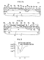
- the relative concentrations as a function of depth of the emitter-base and base-collector junctions in the device are shown in Figure 3.
- the peak concentration of the emitter is 2 x 10 20 /cm 3 while the peak concentration of the base is about 2 x 10 18 /cm 3 .
- the result is a very fast NPN transistor with a very shallow, high-gradient base profile. Any channelling along the sidewall of island 25b will be eliminated with the added concentration of P type impurity along the sidewall due to the ICEO implant.
- the emitter etch is typically 4 minutes or less to prevent the emitter from poking out in front of the base along the sidewall by removal of the field oxide 14b, 14c down to and below the base 25d.
- the diffused field predeposition is replaced with an ion implant, and nitride is used as a shadow mask to prevent the sidewall from being doped, vertical isolation is achieved whereby certain active regions of devices are separated from the underlying channel stop regions.
- the rather shallow base implant for region 25d and the relatively high phosphorous pile-up along the intersection between the isolation oxide and the sidewalls 28a, 28b, 28c and 28d of silicon islands 25a, 25b thus achieves isolation by turning to advantage what previously was considered a disadvantage of oxide isolation techniques (the pile-up of phosphorous impurities in front of thermally grown oxide).
- the lateral PNP transistor as represented by emitter 25c and collector 25d with epitaxial material 15a ( Figure 1) or 25a ( Figure 2) serving as the base, replaces the previous non-active load resistor used in the circuit.
- FIG. 4a A PROM cell constructed in accordance with this invention is shown in Figure 4a.
- P type substrate 41 has formed in it N+ buried layer 42.
- Formed over the top surface of substrate 41 is an epitaxial layer with N type impurity concentration.
- an epitaxial region 43 comprising part of the collector of the device, a floating P type base region 44 and an N+ emitter region 45.
- Collector sink 46 is shown as a hard collector sink. In some situations sink 46 can be a soft collector sink depending upon the requirements of the memory cell.
- the advantage of the structure shown in Figure 4a is that only a collector contact and an emitter contact need be formed to the device thereby reducing the cell size by eliminating the base contact area.
- the structure shown in Figure 4a is formed in the manner described above in conjunction with the structures in Figures 2a through 2d with appropriate modifications to reflect the absence of the lateral transistor.
- the process is suitable for use to form programmable read-only memories because the elimination of the field predeposition increases the NPN base-collector breakdown voltage of the structure.
- Prior art oxide isolated structures have a breakdown voltage of about 16 volts. By eliminating the diffusion in the sidewalls, the breakdown .voltage from collector to base with emitter open (BV CBO ) is raised to 23 to 27 volts. This allows the structure to sustain the voltage necessary to destroy the base-emitter junction (between emitter 45 and base 44 in Figure 4a) because the current necessary to destroy the base-emitter junction depends upon the size of the emitter.
- the emitter size can be controlled to an accuracy of ⁇ 1/2p by controlling the isolation oxide size.
- the emitter 45 is walled on four sides in the PROM memory cell application (no base contact is needed to the device because the base is allowed toifloat in this embodiment) and, therefore, when oxide encroachment is taken into account, a 6x6 micron silicon island 43 becomes, in the active device, about 2-1/2x2-1/2 microns in size. This reduction in size substantially increases the packing density achieved using the process of this invention and by decreasing chip size increases yield.
- BV CBO is roughly 23 to 27 volts, the current sufficient to destroy the emitter-base junction can be generated in the structure.
- n 3 to 4 for silicon.
- an extra mask and implant is utilized only in the memory cell to depress beta, thus raising LV CEO . This aids in increasing programming yields for PROMs.
- the vertical isolation is achieved by the use of N epitaxial material (1.5 to 3 ohms-cm) with no field predeposition along the sidewall.
- the P type base 25d formed in the N epitaxial layer is not allowed to reach the underlying P type 1-1/2 to 3 ohm-cm substrate, thus preventing leakage from the P type base to the P type substrate.
- the substrate will not diffuse upward into the epitaxial layer since both dopant concentrations are approximately equal, i.e. about 1x10 +16 /cm 3 .
- a lower resistivity substrate typically 0.4-0.6 ohm-cm
- the P type impurity to diffuse upward into the epitaxial layer (about 0.6-0.7p for 0.4-0.6 ohm-cm substrate) since the substrate dopant concentration now exceeds that of the epitaxial layer.
- this upward diffusion is sufficient to contact the lower portion of the base, thus ruining vertical isolation.
- the lateral PNP base ( Figure 2d) is reverse biased with respect to the substrate; therefore, parasitic hole injection occurs which is picked up in the substrate. This charge must be eliminated to prevent interference with the $ stack which is referenced above the substrate. Otherwise, the product made using this structure may suffer from "floating" q stacks at high current injection and thus become unstable. Either a gold alloy through the back side of the wafer for contact or contact to the substrate via a ground tap P type implanted sinker from the top surface achieves this. The latter case requires an additional masking step.
- an active PNP cell can be made using one masking step.
- epitaxial resistors are well-controlled because they are implanted.
- a problem can occur with critical dimensions. While the prccess makes a very good 6-micron wide resistor (which with oxide encroachment will reduce down to 2 microns wide) by using the latest state of the art photolithographic.techniques, this resistor can be fabricated down to 1 micron wide after oxide encroachment.
- the soft sink uses N epitaxial material as the sink. Because there is no field predepcsition of impurities along the sidewalls of this sink, the soft sink can be made smaller by approximately 2 microns per dimension than prior art sinks because it will not be pinched off by the encroachment of the field predeposition impurities during oxidation.
- Figure 2d illustrates in dashed line an optional embodiment wherein buried layer 22 terminating prior to contact with the left most field oxide 14a.
- the space 22a represents a PN junction between the P type substrate 11 and the N type epitaxial layer 25.
- P type region 25c is forward-biased relative to N type epitaxial layer portion 25a and thus the P type substrate 11 in combination with N type region 25a and P type region 25c acts as a transistor with possible substantial gain.
- buried layer 22 can, if desired, and indeed should in some applications, extend all the way into contact with the field isolation oxide 14a, as shown. Thus, buried layer 22 would contact and overwhelm a portion of P plus region 23a as shown in Figure 2d.
- the yield in die per wafer has increased an average of about one order of magnitude as a result of use of this process.
- FIG 4b shows the structure of Figure 4a in top view with, however, a modification wherein each collector sink 46, 46-1, 46-2 and 46-3 ( Figures 4a and 4b) is used to provide electrical contact to two active devices rather than one active device.
- collector sink C2 (46-2) makes electrical contact to the active devices including emitters E2 and E3 (numbered 45-2 and 45-3 in Figure 4b).
- Buried layer 42-2 allows electrical contact from collector sink 46-2 to the two devices containing emitters E2 and E3 underneath "the isolation oxide 47 surrounding each of these two active devices. Oxide 47 defines the lateral extent of these devices.
- Bit lines Bl, B2, B3 and B4 are shown running vertically in the drawing. Bit lines Bl to B4 are formed on insulation over the surface of the device. Each bit line is electrically connected to those emitters underlying it through oxide cut contacts. For simplicity, these contacts are not shown in Figure 4b.
- the bit lines B1 to B4 comprise. the first conducting layer on the structure.
- a second layer of insulation is then placed over bit lines Bl to B4 (which typically are fabricated from metal but could also be fabricated of other conductive material such as selectively doped polycrystalline silicon).
- On top of the second layer of insulation typically a phosphorus doped silicon dioxide or silicon dioxide-silicon nitride composite layer
- Word line Wl is shown in Figure 4b extending horizontally across the paper. Each word line contacts those collector regions underlying it through vias such as vias 49-1 through 49-3 as shown in Figure 4b.
- each sink (such as Cl) contacts four active devices (such as El, E2, E3 and E4), two on each side of the sink, thereby further improving packing density.
- active devices such as El, E2, E3 and E4
- up to N active devices can be contacted by each sink, where N is a selected positive integer limited by the voltage drop acceptable in the circuit.
- FIG. 4c Another embodiment of this invention similarly improving packing density by using one collector sink to contact two or more active devices is illustrated in Figure 4c.
- the collector sink regions Cl, C2 corresponding to region 46 in Figure 4a are shown arranged horizontally across the top portion of the drawing.
- Word line Wl extends horizontally across the structure electrically contacting the underlying sink regions through vias 59-1, 59-2.
- the devices containing emitter regions El and E2 are electrically connected to the corresponding collector sink region Cl by a buried layer 42 (shown in isometric cut-away view in Figure 4d) underneath the isolation oxide 47 separating the emitter regions from the collector sink regions.
- Emitter regions E3 and E4 are electrically connected to collector sink region C2 by a buried contact layer similar to layer 42 shown in Figure 4d.
- Bit lines Bl to B4 are formed on insulation overlying the top surface of the structure and make contact to underlying emitter regions El to E4 through oxide cut contacts 60-1 through 60-4 formed through this insulation.
- Word line Wl is formed on insulation overlying bit lines Bl to B4.
- An advantage of this invention is that the oxide cut contacts 60-1 to 60-4 can each overlie a portion of the field oxide 47 so long as a portion of each contact exposes the underlying emitter region. This allows a greater tolerance on the separation of the bit lines B1, B2, B3 and B4 than would otherwise be expected for a structure with as large a packing density as achieved with this structure.
- Each bit line contacts a plurality of underlying emitter regions associated with other cells in a manner such as described above for emitters El to E4 in Figure 4b.
- a second layer of insulation typically a phosphorus doped silicon dioxide or a composite layer of silicon oxide and silicon nitride
- Word line Wl contacts a plurality of underlying collector sinks shown as Cl and C2 in Figure 4c through vias such as vias 59-1 and 59-2 as shown in Figure 4c.
- Each word line contacts the plurality of collector sinks formed beneath the word line through vias such as shown in Figure 4c.
- Figure 4d shows an isometric cut-away view of a portion of the structure shown in Figure 4c along section 4d.
- Figure 4d shows the relationship of a P-type silicon substrate 41 to the other regions formed in the substrate.
- N+ buried layer 42 extends underneath emitter El and collector sink Cl as shown and similarly under emitter E2 (not shown).
- Field oxide 47 defines the lateral extent cf emitter El and collector sink Cl on all sides. Buried contact layer 42 extends underneath field oxide 47 to connect electrically emitter El to collector sink Cl.
- Collector sink Cl is a hard sink having been converted to N+ conductivity type from its normal N conductivity type.
- N epitaxial layer 43 has formed in it P type base region 44 to which no contact is formed and N+ emitter region 45 to which electrical contact is formed from the top surface of the structure as shown in top view in Figure 4c.
- Figure 4d illustrates clearly the fact that the lateral extents of the collector sink and the emitter regions are defined by the oxide region 47 and shows the important size reductions achievable by eliminating the base contact in the PROM cell.
- the PN junction between base region 44 and emitter region 45 is selectively avalanched to break down this junction in selected transistors in the PROM (which contains a plurality of cells of the type shown in Figure 4a) thereby to form a short circuit. The way in which this is done will be briefly described below.
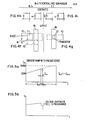
- Figures 4f and 4g show the size reduction achievable by using the structure of this invention as compared to certain prior art NiChrome (nickel-chromium) structures.
- the emitter region 61 is reasonably large and is attached to one end of a fuse link 62, the other end of which is attached to a bit line such as line Bl.
- the emitter region 61 can be. substituted by a base-collector diode or a Schottky.
- bit line Bl is formed of a metal such as aluminum.
- the fuse link 62 will either be left intact thereby leaving a short circuit, or blown, thereby creating an open circuit.
- the fuse linked together with the emitter region takes surface space and reduces packing density.
- Figure 4g illustrates the compact structure of this invention wherein the bit line Bl is directly contacted to the underlying transistor emitter E1 through a contact cut.
- the bit line again is formed of a metal such as aluminum and the buried layer 42 provides electrical contact to the emitter region El from a collector sink (not shown for simplicity).
- Figure 4f prior art
- Figure 4g vertical fuse structure
- Figures 4h and 41 illustrate the circuits resulting from programming the structures of Figures 4f and 4g, respectively.
- FIGs 5a through 5f The programming procedure for programming the FROM cell of this invention is illustrated in Figures 5a through 5f.
- the programming current as a function of time is illustrated for use with the "vertical fuse" (i.e. short-circuited or “blown") emitter structure shown, for example, in Figures 4a through 4g.
- the optimum programming process is one which is insensitive tc design and process variations on the product and which delivers the optimum amount of power to the cell to be programmed.
- the programming structure and method must be sensitive to the avalanching of the emitter-base junction so as to minimize damage to the base-collector junction of the device being programmed.
- the current source used to deliver the programming power must reduce power after the avalanching of the junction and must automatically shut off power after the cell has been "programmed" (i.e., the emitter-base junction destroyed) with a selected delay time. If during programming the base collector junction of a cell is damaged, then leakage may occur through that cell when another cell is being read. Typically the leakage path goes from the bit line attached to the selected cell through to the word line attached to a non-selected or "de-selected" cell, through the damaged base collector junction of this de-selected cell to the bit line attached to this de-selected cell and then through another cell attached to the word line connected to the selected cell. Naturally, this leakage is undesirable.
- a similar leakage path is generated by an abnormally low LVCEO in a de-selected cell. Again, this leakage path is undesirable (this leakage can prevent proper programming of the PROM) and thus proper device processing to prevent low LV CEO in a cell is essential to avoid the identical type of leakage to that caused by a damaged base-collector junction.
- a variable width constant current cell wherein the pulse width was adjusted according to the requirements of each cell yielded good base-collector junctions.
- the programming current required was dependent on design and process variations. Accordingly, it was decided to prcgram each cell with a current source ramping up in time. The duration of the ramping current pulse was variable, dependent upon when the emitter-base junction blew out. The ramping current source made possible easy detection of the blowing of this junction.
- the programming current using this technique is self-adjusting to the needs of each cell. The result is a high programming yield and high reliability of both the programming method and the resulting programmed memory.
- FIG. 5a A current ramp used in conjunction with a voltage sense circuit (of well-known design and thus not described) is illustrated in Figures 5a and 5b.
- a voltage sense circuit detects this drop in voltage across the cell and maintains the current from the current source for a small additional time T ph which varies from 1 to 5 microseconds and then shuts off the current source.
- T ph The maintenance of the current for this additional time Tp h ensures a low resistance programmed cell and at the same time optimizes the power devoted to each cell, thus minimizing the likeli- hcod that the base-collector juncticn of the programmed cell will be damaged. This minimizes the possible occurrence of leakage through the programmed cell when this cell is a de-selected cell connected in the manner described above.
- Another useful technique for programming each cell also uses a series of current pulses as illustrated in Figure 5c.
- the current pulses are generated until a given cell is programmed.
- the total current through the cell is a function of the cell parameters.
- additional K current pulses are provided to ensure low resistance in the programmed cell but not for such a period of time as to damage the base-collector junction.
- the number of pulses need to program each cell varies depending upon the characteristics of each cell.
- Figures 5e and 5f illustrate the memory cell electrical characteristics in the unprogrammed and programmed state, respectively.
- the LV CEO of the cell is about 7.5 volts when the cell is not programmed.
- the back voltage across the diode becomes about 21 volts or greater, corresponding to the voltage breakdown across a collector-base junction using recessed oxide of the type described above in conjunction with Figures 2a-2d.
- the forward bias voltage across the junction is merely about 0.6 to 0.7 volts and the unprogrammed reverse-biased voltage from emitter to collector with the base open is about 3.5 volts as illustrated in Figure 5e.
- Figure 5g illustrates the programming path I-V curve.
- the current voltage path before programming compared to the current voltage path after programming exhibits hysteresis such that after programming the I-V path is displaced substantially to the left on the curve.
- the programming curve Ip is that current at which the cell programs. Once the cell has been programmed, the voltage across the cell drops drastically from about 9 volts as illustrated in Figure 5g to about 15 volts. This plot illustrates the importance of ensuring that LV CEO be greater than 9 volts and, as described above, preferably in excess of 12-15 volts to ensure adequate tolerance for the programming of each cell in the array without exceeding LV CEO .
- the elimination of the boron tube and the low temperature oxidation cycle is the elimination of the boron tube and the low temperature oxidation cycle, the cmission of the base drive step and the elimination of certain mask making steps.
- a field implant is used instead of a field predepositicn followed by low temperature oxidation.
- the additional process steps include an I CEO implant to prevent collector to emitter leakage, and, when PROMS are being made, an additional implant to improve LV CEO .
- an additional advantage is obtained by removing those portions of silicon nitride and silicon oxide layers 24a and 26a ( Figure 2a) in such a manner that the silicon dioxide layer 24a is removed as shown in Figure 2a underneath the lateral extremities of silicon nitride layer 26a. This is done by etching away prior to silicon etch portions of the silicon dioxide layer 24a underneath the lateral extremities of the silicon nitride layer after having patterned silicon nitride layer 26a to expose the regions of epitaxial silicon 25 to be removed to form grooves 27a, 27b and 27c.
- a buffered HF etchant (buffered with ammonium fluoride) is used for this and the wafer is placed in this etchant for times varying from one to eight minutes. Then portions of the epitaxial layer 25 exposed by removal ot the silicon dioxide ana silicon nitrite are etched using a standard silicon etchant (such as an iodine buffered mixture of acetic, nitric and HF acids) to leave a plurality of islands of semiconductor material. The epitaxial silicon is removed laterally beneath the overhangs of the silicon nitride thereby to form sidewalls on the silicon islands recessed beneath the overhangs of the nitride layer 26a by the amount of the removed silicon dioxide.
- a standard silicon etchant such as an iodine buffered mixture of acetic, nitric and HF acids
- the sidewall angle is substantially the same (about 57°) as when the silicon is etched without removal of substantial silicon dioxide. Then the channel stop regions are formed in the bottoms of the grooves 27a, 27b and 27c, laterally displaced from the silicon islands an additional amount determined by the overhang of the silicon nitride layer 26a ever the silicon dioxide layer 24a, thereby to prevent the channel stop regions from laterally diffusing to the silicon islands during subsequent processing of the wafer.
Landscapes
- Semiconductor Memories (AREA)
- Element Separation (AREA)
- Read Only Memory (AREA)
Applications Claiming Priority (2)
| Application Number | Priority Date | Filing Date | Title |
|---|---|---|---|
| US33680282A | 1982-01-04 | 1982-01-04 | |
| US336802 | 1982-01-04 |
Publications (3)
| Publication Number | Publication Date |
|---|---|
| EP0084465A2 true EP0084465A2 (de) | 1983-07-27 |
| EP0084465A3 EP0084465A3 (en) | 1986-02-05 |
| EP0084465B1 EP0084465B1 (de) | 1990-03-21 |
Family
ID=23317735
Family Applications (1)
| Application Number | Title | Priority Date | Filing Date |
|---|---|---|---|
| EP83400012A Expired EP0084465B1 (de) | 1982-01-04 | 1983-01-04 | Oxyd-isolierungsverfahren für Standard RAM/PROM und laterale PNP Zelle RAM |
Country Status (4)
| Country | Link |
|---|---|
| EP (1) | EP0084465B1 (de) |
| JP (1) | JPS58161363A (de) |
| CA (1) | CA1188418A (de) |
| DE (1) | DE3381365D1 (de) |
Cited By (7)
| Publication number | Priority date | Publication date | Assignee | Title |
|---|---|---|---|---|
| DE3312648A1 (de) * | 1982-04-12 | 1983-10-27 | N.V. Philips' Gloeilampenfabrieken, 5621 Eindhoven | Programmierbarer lesespeicher und verfahren zum herstellen desselben |
| DE3437512A1 (de) * | 1983-10-14 | 1985-04-25 | Hitachi Microcomputer Engineering Ltd., Kodaira, Tokio/Tokyo | Integrierte halbleiterschaltung und verfahren zu ihrer herstellung |
| EP0258149A3 (de) * | 1986-08-29 | 1988-10-05 | Fairchild Semiconductor Corporation | Vertikale Sicherung mit schwachddotiertem Emitter |
| US5059555A (en) * | 1990-08-20 | 1991-10-22 | National Semiconductor Corporation | Method to fabricate vertical fuse devices and Schottky diodes using thin sacrificial layer |
| US5144404A (en) * | 1990-08-22 | 1992-09-01 | National Semiconductor Corporation | Polysilicon Schottky clamped transistor and vertical fuse devices |
| US5212102A (en) * | 1990-08-22 | 1993-05-18 | National Semiconductor Corporation | Method of making polysilicon Schottky clamped transistor and vertical fuse devices |
| WO2003069669A1 (en) * | 2002-02-13 | 2003-08-21 | Infineon Technologies Ag | Semiconductor fabrication process, lateral pnp transistor, and integrated circuit |
Family Cites Families (13)
| Publication number | Priority date | Publication date | Assignee | Title |
|---|---|---|---|---|
| US3648125A (en) * | 1971-02-02 | 1972-03-07 | Fairchild Camera Instr Co | Method of fabricating integrated circuits with oxidized isolation and the resulting structure |
| NL7309453A (nl) * | 1973-07-06 | 1975-01-08 | Philips Nv | Geheugenmatrix. |
| US3904450A (en) * | 1974-04-26 | 1975-09-09 | Bell Telephone Labor Inc | Method of fabricating injection logic integrated circuits using oxide isolation |
| DE2554426C3 (de) * | 1975-12-03 | 1979-06-21 | Siemens Ag, 1000 Berlin Und 8000 Muenchen | Verfahren zur Erzeugung einer lokal hohen inversen Stromverstärkung bei einem Planartransistor sowie nach diesem Verfahren hergestellter invers betriebener Transistor |
| JPS5834941B2 (ja) * | 1975-12-11 | 1983-07-29 | 日本電気株式会社 | プログラマブルモノリシツク集積回路 |
| FR2369652A1 (fr) * | 1976-10-29 | 1978-05-26 | Radiotechnique Compelec | Memoire morte programmable a transistors |
| NL7709363A (nl) * | 1977-08-25 | 1979-02-27 | Philips Nv | Werkwijze ter vervaardiging van een halfgeleider- inrichting en halfgeleiderinrichting vervaardigd onder toepassing van een dergelijke werkwijze. |
| US4140558A (en) * | 1978-03-02 | 1979-02-20 | Bell Telephone Laboratories, Incorporated | Isolation of integrated circuits utilizing selective etching and diffusion |
| JPS55127061A (en) * | 1979-03-26 | 1980-10-01 | Hitachi Ltd | Manufacture of semiconductor memory |
| JPS55158665A (en) * | 1979-05-30 | 1980-12-10 | Chiyou Lsi Gijutsu Kenkyu Kumiai | Semiconductor memory storage |
| DE2944141A1 (de) * | 1979-11-02 | 1981-05-14 | Ibm Deutschland Gmbh, 7000 Stuttgart | Monolithisch integrierte speicheranordnung |
| JPS57188865A (en) * | 1981-05-18 | 1982-11-19 | Hitachi Ltd | Semiconductor memory cell |
| JPS57194566A (en) * | 1981-05-27 | 1982-11-30 | Hitachi Ltd | Semiconductor device and manufacture thereof |
-
1982
- 1982-12-31 CA CA000418805A patent/CA1188418A/en not_active Expired
-
1983
- 1983-01-04 EP EP83400012A patent/EP0084465B1/de not_active Expired
- 1983-01-04 JP JP58000016A patent/JPS58161363A/ja active Pending
- 1983-01-04 DE DE8383400012T patent/DE3381365D1/de not_active Expired - Fee Related
Cited By (9)
| Publication number | Priority date | Publication date | Assignee | Title |
|---|---|---|---|---|
| DE3312648A1 (de) * | 1982-04-12 | 1983-10-27 | N.V. Philips' Gloeilampenfabrieken, 5621 Eindhoven | Programmierbarer lesespeicher und verfahren zum herstellen desselben |
| DE3437512A1 (de) * | 1983-10-14 | 1985-04-25 | Hitachi Microcomputer Engineering Ltd., Kodaira, Tokio/Tokyo | Integrierte halbleiterschaltung und verfahren zu ihrer herstellung |
| US4700464A (en) * | 1983-10-14 | 1987-10-20 | Hitachi, Ltd. | Method of forming trench isolation in an integrated circuit |
| EP0258149A3 (de) * | 1986-08-29 | 1988-10-05 | Fairchild Semiconductor Corporation | Vertikale Sicherung mit schwachddotiertem Emitter |
| US5059555A (en) * | 1990-08-20 | 1991-10-22 | National Semiconductor Corporation | Method to fabricate vertical fuse devices and Schottky diodes using thin sacrificial layer |
| US5144404A (en) * | 1990-08-22 | 1992-09-01 | National Semiconductor Corporation | Polysilicon Schottky clamped transistor and vertical fuse devices |
| US5212102A (en) * | 1990-08-22 | 1993-05-18 | National Semiconductor Corporation | Method of making polysilicon Schottky clamped transistor and vertical fuse devices |
| WO2003069669A1 (en) * | 2002-02-13 | 2003-08-21 | Infineon Technologies Ag | Semiconductor fabrication process, lateral pnp transistor, and integrated circuit |
| US7217609B2 (en) | 2002-02-13 | 2007-05-15 | Infineon Technologies Ag | Semiconductor fabrication process, lateral PNP transistor, and integrated circuit |
Also Published As
| Publication number | Publication date |
|---|---|
| DE3381365D1 (de) | 1990-04-26 |
| EP0084465B1 (de) | 1990-03-21 |
| CA1188418A (en) | 1985-06-04 |
| JPS58161363A (ja) | 1983-09-24 |
| EP0084465A3 (en) | 1986-02-05 |
Similar Documents
| Publication | Publication Date | Title |
|---|---|---|
| US4624046A (en) | Oxide isolation process for standard RAM/PROM and lateral PNP cell RAM | |
| US4116720A (en) | Method of making a V-MOS field effect transistor for a dynamic memory cell having improved capacitance | |
| US4261763A (en) | Fabrication of integrated circuits employing only ion implantation for all dopant layers | |
| CA1118532A (en) | Method of manufacturing a semiconductor device | |
| CA1183966A (en) | Method for manufacturing a semiconductor structure having reduced lateral spacing between buried regions | |
| EP0084500B1 (de) | Ionenimplantierte Speicherzellen für hochintegrierte RAM | |
| US4727409A (en) | Programmable read-only memory formed with opposing PN diodes | |
| EP0078725B1 (de) | Verfahren zur Herstellung eines Submikron-Bipolartransistors ohne epitaxiales Wachstum und die sich ergebende Struktur | |
| JP2002522925A (ja) | トレンチゲート半導体装置 | |
| EP0084465B1 (de) | Oxyd-isolierungsverfahren für Standard RAM/PROM und laterale PNP Zelle RAM | |
| US4961102A (en) | Junction programmable vertical transistor with high performance transistor | |
| US4979010A (en) | VLSI self-aligned bipolar transistor | |
| US4225879A (en) | V-MOS Field effect transistor for a dynamic memory cell having improved capacitance | |
| US4933736A (en) | Programmable read-only memory | |
| US5104816A (en) | Polysilicon self-aligned bipolar device including trench isolation and process of manufacturing same | |
| US4945066A (en) | Process for manufacturing a dynamic random access memory cell | |
| US5332683A (en) | Method of manufacturing semiconductor device having elements isolated by trench | |
| US4660278A (en) | Process of making IC isolation structure | |
| US4799099A (en) | Bipolar transistor in isolation well with angled corners | |
| JPS6119171A (ja) | 縦型npnトランジスタ構造体 | |
| US4694566A (en) | Method for manufacturing programmable read-only memory containing cells formed with opposing diodes | |
| EP0231740A2 (de) | Selbstjustierendes bipolares Bauelement aus Polysilizium und Verfahren zu seiner Herstellung | |
| US6806159B2 (en) | Method for manufacturing a semiconductor device with sinker contact region | |
| JPH0618256B2 (ja) | プログラマブル 半 導 体 装 置 | |
| EP0253538B1 (de) | Selbstjustierter VLSI bipolarer Transistor |
Legal Events
| Date | Code | Title | Description |
|---|---|---|---|
| PUAI | Public reference made under article 153(3) epc to a published international application that has entered the european phase |
Free format text: ORIGINAL CODE: 0009012 |
|
| AK | Designated contracting states |
Designated state(s): DE FR GB IT NL |
|
| PUAL | Search report despatched |
Free format text: ORIGINAL CODE: 0009013 |
|
| AK | Designated contracting states |
Designated state(s): DE FR GB IT NL |
|
| 17P | Request for examination filed |
Effective date: 19860730 |
|
| 17Q | First examination report despatched |
Effective date: 19871127 |
|
| RAP1 | Party data changed (applicant data changed or rights of an application transferred) |
Owner name: FAIRCHILD SEMICONDUCTOR CORPORATION |
|
| GRAA | (expected) grant |
Free format text: ORIGINAL CODE: 0009210 |
|
| AK | Designated contracting states |
Kind code of ref document: B1 Designated state(s): DE FR GB IT NL |
|
| REF | Corresponds to: |
Ref document number: 3381365 Country of ref document: DE Date of ref document: 19900426 |
|
| ET | Fr: translation filed | ||
| ITF | It: translation for a ep patent filed | ||
| PLBE | No opposition filed within time limit |
Free format text: ORIGINAL CODE: 0009261 |
|
| STAA | Information on the status of an ep patent application or granted ep patent |
Free format text: STATUS: NO OPPOSITION FILED WITHIN TIME LIMIT |
|
| ITTA | It: last paid annual fee | ||
| 26N | No opposition filed | ||
| PGFP | Annual fee paid to national office [announced via postgrant information from national office to epo] |
Ref country code: GB Payment date: 19931220 Year of fee payment: 12 |
|
| PGFP | Annual fee paid to national office [announced via postgrant information from national office to epo] |
Ref country code: FR Payment date: 19940111 Year of fee payment: 12 |
|
| PGFP | Annual fee paid to national office [announced via postgrant information from national office to epo] |
Ref country code: NL Payment date: 19940131 Year of fee payment: 12 |
|
| PG25 | Lapsed in a contracting state [announced via postgrant information from national office to epo] |
Ref country code: GB Effective date: 19950104 |
|
| PG25 | Lapsed in a contracting state [announced via postgrant information from national office to epo] |
Ref country code: NL Effective date: 19950801 |
|
| GBPC | Gb: european patent ceased through non-payment of renewal fee |
Effective date: 19950104 |
|
| PG25 | Lapsed in a contracting state [announced via postgrant information from national office to epo] |
Ref country code: FR Effective date: 19950929 |
|
| NLV4 | Nl: lapsed or anulled due to non-payment of the annual fee |
Effective date: 19950801 |
|
| REG | Reference to a national code |
Ref country code: FR Ref legal event code: ST |
|
| PGFP | Annual fee paid to national office [announced via postgrant information from national office to epo] |
Ref country code: DE Payment date: 19970129 Year of fee payment: 15 |
|
| PG25 | Lapsed in a contracting state [announced via postgrant information from national office to epo] |
Ref country code: DE Free format text: LAPSE BECAUSE OF NON-PAYMENT OF DUE FEES Effective date: 19981001 |