EP0084675A2 - Procédé et dispositif pour la synchronisation d'horloge au côté de réception d'un système de transmission plésiochrone - Google Patents
Procédé et dispositif pour la synchronisation d'horloge au côté de réception d'un système de transmission plésiochrone Download PDFInfo
- Publication number
- EP0084675A2 EP0084675A2 EP82111963A EP82111963A EP0084675A2 EP 0084675 A2 EP0084675 A2 EP 0084675A2 EP 82111963 A EP82111963 A EP 82111963A EP 82111963 A EP82111963 A EP 82111963A EP 0084675 A2 EP0084675 A2 EP 0084675A2
- Authority
- EP
- European Patent Office
- Prior art keywords
- circuit
- input
- clock signal
- signal
- output
- Prior art date
- Legal status (The legal status is an assumption and is not a legal conclusion. Google has not performed a legal analysis and makes no representation as to the accuracy of the status listed.)
- Granted
Links
Images

Classifications
-
- H—ELECTRICITY
- H04—ELECTRIC COMMUNICATION TECHNIQUE
- H04J—MULTIPLEX COMMUNICATION
- H04J3/00—Time-division multiplex systems
- H04J3/02—Details
- H04J3/06—Synchronising arrangements
- H04J3/07—Synchronising arrangements using pulse stuffing for systems with different or fluctuating information rates or bit rates
Definitions
- the primary clock can be matched to the transmitting side on the receiving side in a phase locked loop only if the stuffing identification word in which the information of the clock adaptation is transmitted is not disturbed .
- phase-locked loop no longer receives a clear control criterion.
- the receive clock moves away from its prescribed tolerance limit.
- the stuffing identification word is distributed redundantly in the frame structures of the digital signal multiplex devices.
- the stuffing identification word consists of three bits each in the secondary and tertiary systems and even five bits in the quaternary and quaternary system. Because when evaluating the A majority decision is made, it can even be faulty to a certain extent.
- tuft disorders can occur in such a way that the frame identifier is disturbed and the frame identifier can fail. In this case the receiving side can no longer correctly recognize the stuffing identification word and the frequency of the signal from the phase locked loop can break out of its prescribed tolerance range. In the systems mentioned, an AIS (alarm indication signal) is then sent out. It must be avoided that the frequencies of the clock signals of the phase-locked loop leave the prescribed tolerances in the event of failure as well as when the frame identifier re-enters, so that downstream regenerator sections remain clock-synchronized.
- AIS alarm indication signal
- the recovered, channel-related, discontinuous reception clock signal Tm caused by system parameters must be converted into a continuous clock signal TE with the aid of the phase locked loop.
- the receiving side can no longer correctly evaluate the stuffing identifier word. In any case, care must be taken to ensure that both the AIS transmitted at the start of the alarm and the information signal replacing the AIS at the end of the alarm are within the prescribed tolerance limits of the bit repetition frequencies.
- the invention is based on the object of specifying a method of the type mentioned at the outset with which it is possible to determine the frequency of the reception clock even during faults in which the stuffing identification word can no longer be recognized on the reception side, in particular when the alarm starts and ends Te) to get exactly.
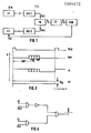
- phase detector PD One is obtained from the continuous clock signal TE via the counter Z2 and decoding DEC2, the other from the discontinuous clock signal Tm originating from the demultiplexer via the counter Z1 and decoding DEC1.
- Fig. 2 shows the timing diagram of the phase detector of the control loop.
- the phase comparison signal Phl derived from the discontinuous clock signal Tm has a system jitter and, due to the control principle of the loop, has a phase shift of 180 ° ⁇ ⁇ ⁇ with respect to the signal Ph2, which is freed from this jitter.
- the phase detector PD which is activated by the comparison signals Ph1 and Ph2, represents nothing other than a bistable element.
- the phase fluctuation range of the output signal A is symmetrical to the center of the comparison signal Ph2 (FIG. 2).
- the jittered output signal A of the phase detector PD is freed of this jitter in the subsequent low-pass filter and integrated to its half amplitude value A / 2.
- the nominal frequency of the clock signal TE is set.
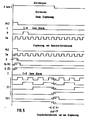
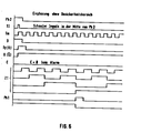
- the low-pass filter also forms half the amplitude value A / 2 and the nominal frequency is again set (FIGS. 3 and 5 ).
- the phase locked loop no longer works according to a control criterion, but according to the absolute amount A / 2.
- phase comparison signal Ph 1 derived from this can lie anywhere within the step duration of the phase comparison signal Ph2.
- the phase detector signal can thus assume any duty cycle. Since these can be large, the filter capacitors of the phase-locked loop experience larger charges.
- the asymmetrical duty cycle is gradually reduced by the control process of the loop. A settling process takes place which, depending on the duty cycle, generates control voltage jumps which can be so great that the associated frequency changes far exceed the predetermined tolerance range of the oscillator frequencies.
- FIGS 3 and 5 illustrate the process of phasing.
- the alarm signal C goes to zero and releases the bistable element U.
- the bistable element Sy is set (reset by D). This activates the element U, which switches through the output signal A of the phase detector to the output E of the clock switch TU and on the other hand releases the counter Z1 which has been blocked up to now.
Landscapes
- Engineering & Computer Science (AREA)
- Computer Networks & Wireless Communication (AREA)
- Signal Processing (AREA)
- Synchronisation In Digital Transmission Systems (AREA)
- Stabilization Of Oscillater, Synchronisation, Frequency Synthesizers (AREA)
Applications Claiming Priority (2)
| Application Number | Priority Date | Filing Date | Title |
|---|---|---|---|
| DE19823202540 DE3202540A1 (de) | 1982-01-27 | 1982-01-27 | Verfahren und anordnung zur taktsynchronisierung auf der empfangsseite eines plesiochronen uebertragungssytems |
| DE3202540 | 1982-01-27 |
Publications (3)
| Publication Number | Publication Date |
|---|---|
| EP0084675A2 true EP0084675A2 (fr) | 1983-08-03 |
| EP0084675A3 EP0084675A3 (en) | 1984-09-19 |
| EP0084675B1 EP0084675B1 (fr) | 1987-03-11 |
Family
ID=6154011
Family Applications (1)
| Application Number | Title | Priority Date | Filing Date |
|---|---|---|---|
| EP82111963A Expired EP0084675B1 (fr) | 1982-01-27 | 1982-12-23 | Procédé et dispositif pour la synchronisation d'horloge au côté de réception d'un système de transmission plésiochrone |
Country Status (2)
| Country | Link |
|---|---|
| EP (1) | EP0084675B1 (fr) |
| DE (2) | DE3202540A1 (fr) |
Cited By (1)
| Publication number | Priority date | Publication date | Assignee | Title |
|---|---|---|---|---|
| WO1991012678A1 (fr) * | 1990-02-16 | 1991-08-22 | Siemens Aktiengesellschaft | Procede et dispositif de recuperation du rythme |
Family Cites Families (6)
| Publication number | Priority date | Publication date | Assignee | Title |
|---|---|---|---|---|
| DE2204703C3 (de) * | 1971-02-22 | 1981-05-27 | Società Italiana Telecomunicazioni Siemens S.p.A., 20149 Milano | Schaltungsanordnung zum Einführen eines Ersatz-Taktsignals in ein PCM-Übertragungssystem |
| US3940558A (en) * | 1975-01-31 | 1976-02-24 | Digital Communications Corporation | Remote master/slave station clock |
| DE2622418C2 (de) * | 1976-05-19 | 1978-06-01 | Siemens Ag, 1000 Berlin Und 8000 Muenchen | Anordnung zum empfangsseitigen Rückgewinnen von Takten mehrerer in einem Pulsrahmen mittels Positiv-Negativ-Stopfens verschachtelter Digitalsignale |
| IT1074199B (it) * | 1976-12-23 | 1985-04-17 | Italiana Telecomunicazioni Ora | Memoria elastica per la soppressione del disturbo di fase (jitter)nei sistemi di trasmissione per segnali digitali |
| DE2824137C2 (de) * | 1978-06-02 | 1980-06-26 | Siemens Ag, 1000 Berlin Und 8000 Muenchen | Einrichtung zur Phasensynchronisation |
| DE2920809A1 (de) * | 1979-05-22 | 1980-11-27 | Siemens Ag | Verfahren und schaltungsanordnung zur synchronisierung bei der uebertragung von digitalen nachrichtensignalen |
-
1982
- 1982-01-27 DE DE19823202540 patent/DE3202540A1/de not_active Withdrawn
- 1982-12-23 DE DE8282111963T patent/DE3275690D1/de not_active Expired
- 1982-12-23 EP EP82111963A patent/EP0084675B1/fr not_active Expired
Cited By (2)
| Publication number | Priority date | Publication date | Assignee | Title |
|---|---|---|---|---|
| WO1991012678A1 (fr) * | 1990-02-16 | 1991-08-22 | Siemens Aktiengesellschaft | Procede et dispositif de recuperation du rythme |
| US5426672A (en) * | 1990-02-16 | 1995-06-20 | Siemens Aktiengesellschaft | Process and device for timing recovery |
Also Published As
| Publication number | Publication date |
|---|---|
| DE3202540A1 (de) | 1983-08-04 |
| EP0084675A3 (en) | 1984-09-19 |
| DE3275690D1 (en) | 1987-04-16 |
| EP0084675B1 (fr) | 1987-03-11 |
Similar Documents
| Publication | Publication Date | Title |
|---|---|---|
| DE3728022C2 (fr) | ||
| DE69627849T2 (de) | Verteilung der synchronisation in einer synchronen optischen umgebung | |
| DE69513088T2 (de) | Einrichtung zum Ableiten eines Taktsignals | |
| DE69123473T2 (de) | Schaltungsanordnung zum Ableiten eines Bitsynchronisierungssignals mittels Rahmensynchronisation | |
| DE3215783C2 (de) | Digitale Datenübertragungsanlage mit störungsfreiem Umschalten von regulären Kanälen auf einen Reservekanal | |
| DE2901235A1 (de) | Digitales zweidraht-vollduplex- uebertragungssystem | |
| DE2703395B2 (de) | Schaltungsanordnung zum Rückgewinnen kodierter Binärinformation | |
| DE69103769T2 (de) | Ausrichtung der phase eines taktsignals. | |
| DE1537638B2 (de) | Übertragungssystem mit einer Sende- und einer Empfangsvorrichtung zur Übertragung von Informationen in einem vorgeschriebenen Frequenzband sowie dabei zu verwendende Sende- und Empfangsvorrichtungen | |
| EP0009586B1 (fr) | Procédé pour la synchronisation de dispositifs d'émission et de réception | |
| DE2757285A1 (de) | Vorrichtung zum empfangen von in form einer vielzahl von bits uebertragenen information | |
| DE69111669T2 (de) | Phasenkorrekturschaltung für Signale in einem System mit doppelten digitalen Leitungen. | |
| DE3309270A1 (de) | Synchronisation nachziehbarer taktoszillatoren bei der uebertragung digitaler signale | |
| DE69225320T2 (de) | Adapter zum Anschluss an ein "clear channel"-Übertragungsnetz | |
| DE3217584A1 (de) | Digitales pcm-uebertragungssystem | |
| DE2855082A1 (de) | Uebertragungssystem fuer digitale signale | |
| EP0084675B1 (fr) | Procédé et dispositif pour la synchronisation d'horloge au côté de réception d'un système de transmission plésiochrone | |
| DE3924283A1 (de) | Schaltungsanordnung zur durchschaltung eines digitalen dienstkanals in einer richtfunk-zwischenstelle | |
| DE69002086T2 (de) | Anordnung zur Synchronisation eines pseudobinären Signals mit einem durch Phasensprung regenerierten Taktsignal. | |
| DE1537012A1 (de) | Netzwerksynchronisation in einem Zeitmultiplex-Vermittlungssystem | |
| DE3245438C2 (de) | Frequenzsensitive Phasenregelschleife | |
| EP0419895A2 (fr) | Méthode d'alimentation d'horloge pour les systèmes multiplexes | |
| DE2427603A1 (de) | Schaltungsanordnung zum nachbilden der wellenform von telegrafieschrittimpulsen mit digitalen mitteln | |
| EP0241777B1 (fr) | Etage de démultiplexage d'un appareil de transmission de signaux numériques | |
| CH617051A5 (fr) |
Legal Events
| Date | Code | Title | Description |
|---|---|---|---|
| PUAI | Public reference made under article 153(3) epc to a published international application that has entered the european phase |
Free format text: ORIGINAL CODE: 0009012 |
|
| AK | Designated contracting states |
Designated state(s): BE DE FR GB IT NL |
|
| RAP1 | Party data changed (applicant data changed or rights of an application transferred) |
Owner name: ANT NACHRICHTENTECHNIK GMBH |
|
| PUAL | Search report despatched |
Free format text: ORIGINAL CODE: 0009013 |
|
| AK | Designated contracting states |
Designated state(s): BE DE FR GB IT NL |
|
| 17P | Request for examination filed |
Effective date: 19841214 |
|
| ITF | It: translation for a ep patent filed | ||
| GRAA | (expected) grant |
Free format text: ORIGINAL CODE: 0009210 |
|
| AK | Designated contracting states |
Kind code of ref document: B1 Designated state(s): BE DE FR GB IT NL |
|
| REF | Corresponds to: |
Ref document number: 3275690 Country of ref document: DE Date of ref document: 19870416 |
|
| ET | Fr: translation filed | ||
| PLBE | No opposition filed within time limit |
Free format text: ORIGINAL CODE: 0009261 |
|
| STAA | Information on the status of an ep patent application or granted ep patent |
Free format text: STATUS: NO OPPOSITION FILED WITHIN TIME LIMIT |
|
| 26N | No opposition filed | ||
| ITTA | It: last paid annual fee | ||
| PGFP | Annual fee paid to national office [announced via postgrant information from national office to epo] |
Ref country code: FR Payment date: 19921214 Year of fee payment: 11 |
|
| PGFP | Annual fee paid to national office [announced via postgrant information from national office to epo] |
Ref country code: GB Payment date: 19921216 Year of fee payment: 11 |
|
| PGFP | Annual fee paid to national office [announced via postgrant information from national office to epo] |
Ref country code: BE Payment date: 19921224 Year of fee payment: 11 |
|
| PGFP | Annual fee paid to national office [announced via postgrant information from national office to epo] |
Ref country code: NL Payment date: 19921231 Year of fee payment: 11 |
|
| PGFP | Annual fee paid to national office [announced via postgrant information from national office to epo] |
Ref country code: DE Payment date: 19930210 Year of fee payment: 11 |
|
| PG25 | Lapsed in a contracting state [announced via postgrant information from national office to epo] |
Ref country code: GB Effective date: 19931223 |
|
| PG25 | Lapsed in a contracting state [announced via postgrant information from national office to epo] |
Ref country code: BE Effective date: 19931231 |
|
| BERE | Be: lapsed |
Owner name: ANT NACHRICHTENTECHNIK G.M.B.H. Effective date: 19931231 |
|
| PG25 | Lapsed in a contracting state [announced via postgrant information from national office to epo] |
Ref country code: NL Effective date: 19940701 |
|
| NLV4 | Nl: lapsed or anulled due to non-payment of the annual fee | ||
| GBPC | Gb: european patent ceased through non-payment of renewal fee |
Effective date: 19931223 |
|
| PG25 | Lapsed in a contracting state [announced via postgrant information from national office to epo] |
Ref country code: FR Effective date: 19940831 |
|
| PG25 | Lapsed in a contracting state [announced via postgrant information from national office to epo] |
Ref country code: DE Effective date: 19940901 |
|
| REG | Reference to a national code |
Ref country code: FR Ref legal event code: ST |