EP0084876A2 - Montage démodulateur pour signaux modulés en fréquence sur une onde porteuse - Google Patents
Montage démodulateur pour signaux modulés en fréquence sur une onde porteuse Download PDFInfo
- Publication number
- EP0084876A2 EP0084876A2 EP83100559A EP83100559A EP0084876A2 EP 0084876 A2 EP0084876 A2 EP 0084876A2 EP 83100559 A EP83100559 A EP 83100559A EP 83100559 A EP83100559 A EP 83100559A EP 0084876 A2 EP0084876 A2 EP 0084876A2
- Authority
- EP
- European Patent Office
- Prior art keywords
- mixer
- output
- frequency
- circuit
- demodulator
- Prior art date
- Legal status (The legal status is an assumption and is not a legal conclusion. Google has not performed a legal analysis and makes no representation as to the accuracy of the status listed.)
- Withdrawn
Links
- 239000003990 capacitor Substances 0.000 claims description 5
- 235000014366 other mixer Nutrition 0.000 abstract 1
- 238000000034 method Methods 0.000 description 13
- 230000014509 gene expression Effects 0.000 description 7
- 230000003321 amplification Effects 0.000 description 4
- 238000003199 nucleic acid amplification method Methods 0.000 description 4
- 238000010586 diagram Methods 0.000 description 3
- 230000000694 effects Effects 0.000 description 3
- 230000001105 regulatory effect Effects 0.000 description 3
- 230000005540 biological transmission Effects 0.000 description 2
- 230000001276 controlling effect Effects 0.000 description 2
- 230000036962 time dependent Effects 0.000 description 2
- 238000003491 array Methods 0.000 description 1
- 238000004519 manufacturing process Methods 0.000 description 1
- 230000010355 oscillation Effects 0.000 description 1
- 230000035945 sensitivity Effects 0.000 description 1
- 238000000926 separation method Methods 0.000 description 1
- 230000005236 sound signal Effects 0.000 description 1
- 230000006641 stabilisation Effects 0.000 description 1
- 238000011105 stabilization Methods 0.000 description 1
Images

Classifications
-
- H—ELECTRICITY
- H03—ELECTRONIC CIRCUITRY
- H03G—CONTROL OF AMPLIFICATION
- H03G3/00—Gain control in amplifiers or frequency changers
- H03G3/20—Automatic control
- H03G3/30—Automatic control in amplifiers having semiconductor devices
- H03G3/3052—Automatic control in amplifiers having semiconductor devices in bandpass amplifiers (H.F. or I.F.) or in frequency-changers used in a (super)heterodyne receiver
-
- H—ELECTRICITY
- H03—ELECTRONIC CIRCUITRY
- H03D—DEMODULATION OR TRANSFERENCE OF MODULATION FROM ONE CARRIER TO ANOTHER
- H03D3/00—Demodulation of angle-, frequency- or phase- modulated oscillations
- H03D3/007—Demodulation of angle-, frequency- or phase- modulated oscillations by converting the oscillations into two quadrature related signals
-
- H—ELECTRICITY
- H03—ELECTRONIC CIRCUITRY
- H03J—TUNING RESONANT CIRCUITS; SELECTING RESONANT CIRCUITS
- H03J7/00—Automatic frequency control; Automatic scanning over a band of frequencies
- H03J7/02—Automatic frequency control
-
- H—ELECTRICITY
- H03—ELECTRONIC CIRCUITRY
- H03D—DEMODULATION OR TRANSFERENCE OF MODULATION FROM ONE CARRIER TO ANOTHER
- H03D7/00—Transference of modulation from one carrier to another, e.g. frequency-changing
- H03D7/16—Multiple-frequency-changing
- H03D7/161—Multiple-frequency-changing all the frequency changers being connected in cascade
- H03D7/163—Multiple-frequency-changing all the frequency changers being connected in cascade the local oscillations of at least two of the frequency changers being derived from a single oscillator
-
- H—ELECTRICITY
- H03—ELECTRONIC CIRCUITRY
- H03D—DEMODULATION OR TRANSFERENCE OF MODULATION FROM ONE CARRIER TO ANOTHER
- H03D7/00—Transference of modulation from one carrier to another, e.g. frequency-changing
- H03D7/16—Multiple-frequency-changing
- H03D7/165—Multiple-frequency-changing at least two frequency changers being located in different paths, e.g. in two paths with carriers in quadrature
Definitions
- the invention relates to a demodulator arrangement for demodulating signals contained in frequency modulation on a carrier frequency wave of the type specified in the preamble of claim 1.
- the so-called zero IF technology brought about a significant breakthrough for the production of such receivers.
- the output signal of the two mixing circuits contains two side bands folded on top of each other on a zero-ZR carrier extend from 0 to the bandwidth of the single sideband of the signal modulated on the incoming carrier.
- the output signals of the mixed circuits are passed to amplifiers via low-pass filters, in which they are amplified to a predetermined value.
- the output signals of the amplifiers are then differentiated.
- the output signal of each of the differentiating circuits is multiplied by the input signal of the other differentiating circuit, and the difference is formed from the output signals of the two multiplier circuits.
- Such a method is also known from US Pat. No. 4,238,850.
- phased-locked-loop demodulators are used which are tuned to the frequency of the carrier frequency wave.
- the local oscillator of such an arrangement follows the useful signal and the tuning voltage for such a local oscillator therefore runs proportionally to the voltage curve of the useful signal, including a constant. If this tuning voltage is decoupled without the constant, the decoupled signal is an image of the envelope curve of the useful signal and therefore represents the modulation.
- phase lock loops prevent steep filters in the carrier channel due to the stability of their properties. Accordingly, the subsequent channel separation is relatively small and such a receiver is very difficult to implement.
- Use taking these disadvantages into account other known arrangements two channels in quadrature. This means that steep filters can be used and the filtered signals can be demodulated.
- one channel is operated in phase and the other in quadrature and this process is called the I + Q process.
- this method works with the carrier frequency wave. It can be used to demodulate double-sideband, single-sideband amplitude-modulated signals as well as frequency-shift keyed signals.
- passive components are used to transmit the carrier frequency waves in receiving devices that work according to the I + Q method, so that they can be demodulated.
- passive components no feedback means can be used to stabilize the receiver.
- each carrier frequency wave signal is differentiated, then must be multiplied with the undifferentiated other signal and then summed.
- the other channel either the I or the Q channel, is treated in a similar manner.
- this process produces noise and distortion.
- Phase deviations in the phase channel and in the quadrature channel also generate noise disturbances and distortions.
- beat tones are generated which cause further disturbances in the transmission process.
- the invention is therefore based on the object of specifying a demodulator arrangement of the type specified at the outset which works with two channels but avoids the disadvantages of the I + Q method.
- This object is achieved according to the invention by the technical features specified in the characterizing part of claim 1.
- the phase division of the local oscillator prevents the disruptive effects of small phase inaccuracies in a demodulator arrangement according to the invention.
- the automatic frequency control prevents disturbing frequency deviations of the demodulator arrangement.
- an automatic gain control can be provided in the demodulator arrangement according to the invention, which allows a greater dynamic range of the arrangement. This measure means that no amplifiers with a high gain are required for the carrier frequency wave. Rather, amplifiers with a fixed gain or amplifiers with a low, adjustable gain can be used in this case. As a result, large feedback factors can be used with these amplifiers, so that the smoothness of the properties and the amplification on the two channels can be improved.
- a demodulator arrangement according to the invention is in its nature an analog circuit. However, it is advantageously designed so that it can be easily manufactured as an integrated circuit.
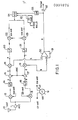
- FIG. 1 shows a schematic block diagram of a receiver with a demodulator arrangement for demodulating signals contained in frequency modulation on a carrier frequency wave.
- a carrier frequency wave onto which a useful signal is modulated in frequency modulation, is received at an antenna 10 and transmitted to the input of a regulating amplifier 11.
- the control amplifier 11 receives at its control input an AGC gain control signal, which is generated in a circuit described below.
- One input of a first mixer circuit 12 and one input of a second mixer circuit 13 are connected to the output of the amplifier 11. At their other input, both mixing circuits 12 and 13 receive an output signal from a Loka Len oscillator 44.
- the local oscillator 44 which may for example be designed in the form of a frequency synthesizer, or other tunable circuit includes a square circuit consisting of the oscillation frequency of a first signal of the form sin w o tt and a second output signal of the GestaLt cos w o t generated. As shown in FIG. 1, the mixer circuit 12 receives the oscillator signal cos w o t and the mixer circuit 13 receives the oscillator signal sin w o t.
- a low-pass filter 14 is connected to the output of the mixer circuit 12 and a low-pass filter 15 to the output of the mixer circuit 13.
- the bandwidth of the two low-pass filters 14 and 15 is designed so that it is at least as wide as the assumed greatest deviation in the frequency of the carrier wave from the frequency of the local oscillator 44. In this way, two signals are obviously produced at the output of the two low-pass filters 14 and 15, which are rotated 90 ° relative to one another by the quadrature. It is essential that the frequency set on the local oscillator 44 for generating the two output signals of the oscillator which are in phase quadrature is equal to the frequency of the carrier waves for the frequency-modulated useful signal. This setting is known from the zero IF method.
- the output a of the low-pass filter 14 is connected to the input of an amplifier 16 and the output b of the low-pass filter 15 is connected to the input of an amplifier 17.
- the amplifiers 16 and 17 also have, for example, a controllable amplification which can be regulated, for example, by the same control signal AGC at their control inputs as the control amplifier 11.
- the output c of the amplifier 16 is at an input a multiplicative mixer circuit 18 is connected while the output d of the amplifier 17 is connected to an input of a multiplicative mixer circuit 19.
- the other input of the mixer circuit 18 is fed by the output e of a low-pass filter 20, while the other input of the mixer circuit 19 is fed by the output f of a low-pass filter 21.
- the input of the low-pass filter 20 is connected to the output of a mixing circuit 22, while the input of the low-pass filter 21 is connected to the output of a mixing circuit 23.
- the mixing circuit 22 receives the signal Sin w o t of the local oscillator 44 at its one input, while the mixing circuit 23 receives the signal cos w 0 t of the local oscillator 44 at its one input.
- the other inputs of the mixer circuits 22 and 23 are fed by a voltage-controlled oscillator 24, the frequency of which can be set.
- the voltage-controlled oscillator 24 has a tuning input 25, at which it receives a tuning direct voltage generated by the local oscillator 44 in order to set a desired frequency.
- the demodulator arrangement has two channels, each with three mixing circuits, an upper channel with the mixing circuits 12, 18 and 22 and a lower channel with the three mixing circuits 13, 19 and 23.
- the output h of the mixing circuit 18 is connected to the non-inverting input of an operational amplifier 30, while the output k of the mixing circuit 19 is connected via a resistor to the inverting input of the operational amplifier 30 denoted by minus.
- the operational amplifier 30 is designed as an integrator and has therefore arranged a capacitor 31 between its output g and its inverting input.
- the AC signal coupled out from the output g of the operational amplifier via a capacitor 32 corresponds to the modulation of the input signal received at the antenna 10.
- the output signal of the operational amplifier 30 regulates the frequency of the voltage-controlled oscillator 24 via a stabilization network 33 and thus ensures that disturbances inherent in the known methods are prevented.
- the frequency control of the voltage-controlled oscillator 24 has the effect that the output signal of the demodulator arrangement is always proportional to the modulation and that errors caused by inequalities between the two channels are suppressed or substantially reduced.
- the frequency w o of the local oscillator 44 is set such that it is normally equal to the carrier frequency w c . This reduces expressions (I) and (II) to: where A and A ° are approximately the same size.
- a tuning voltage is applied to the oscillator 24 via the input 25, which sets the voltage-controlled oscillator 24 to a frequency w a , which is determined by the setting of the local oscillator 44 and which is tight is at the tuning frequency w o of the LokaLen OsziLLator, but not necessarily the same.
- the output signal of the voltage-controlled oscillator 24 is designated by the following expression: where ⁇ is an arbitrary phase in the form of a time-dependent function and D 'is an amplitude
- the signal at the output e of the low pass 20 is then: and at output f of low pass 21: where ⁇ 2 is the setting error for setting the frequency w a .
- the signals at the outputs c and e reach the inputs of the mixer circuit 18. If this works, for example, as a multiplicative mixer, the following signal is generated at its output h:
- the signal is generated at the output k of the mixer circuit 19:
- this signal (VII) represents an error signal in a feedback loop, it is driven towards zero. That can only happen if This condition is met if
- the operational amplifier 30 no longer integrates the error signal ⁇ - ⁇ and ⁇ is then no longer exactly the image of the signal ⁇ . However, if the operational amplifier has a high gain, this error is negligible. However, if the operational amplifier 30 works as an integrator and there can be a voltage at its output, even if the input voltage is NuLL, the deviation can theoretically be driven to NuLL.
- FIG. 2 shows a circuit arrangement for generating a control signal AGC for controlling the amplification of the preamplifier 11 and the amplifiers 16 and 17. Circuit elements adopted from FIG. 1 have the same reference symbols as in FIG. 1.
- the other input signals for the mixer circuits 18 and 19 from the outputs e and f of the low-pass filters 20 and 21 are sent to the inputs of the mixer circuits 18 via a first two-pole electronic switch 40 and 19 placed.
- the switch 40 can be a FET or a MOS circuit, the control electrodes of which are controlled by a source 43 with a high-frequency switching signal.
- the switching frequency of the switching signal is at least two times as high as the highest pass frequency of the FM input signal, according to the NyKvist theory.
- the outputs k and h of the mixer circuits 18 and 19 are connected to the changeover connections of a two-pole electronic changeover switch 41.
- This switch 41 switches the outputs alternately to the inputs of the operational amplifier 30 and the inputs of a second amplifier 45.
- the output of the operational amplifier 30 continues to generate signals proportional to the signal ⁇ and thus a signal representing the modulation signal.
- a direct current signal is produced which is proportional to the amplitude of the waveforms used in the arrangement and which is used directly as a control signal AGC for the gain control.
- the gain control signal AGC is implemented as follows: If the phases of the frequency set ( ⁇ 2) are not inverted by the mixed shades 22 and 23 with respect to the frequency set ( ⁇ 1 ) of the mixer circuits 12 and 13, one obtains:
- the circuit arrangement thus compensates for phase inaccuracies.
- narrow-band or steep filters can be used without loop instabilities occurring.
- the use of a voltage-controlled oscillator enables the mixer circuits 18 and 19 to operate reliably over wide ranges, since it is ensured that the frequency of the voltage-controlled oscillator is safely regulated.
- Errors both in the phase generator as well as in the quadrature circuit of the local oscillator, as well as errors in the useful signal are also compensated for.
- An arrangement with a high switching rate makes it possible to generate a control signal for the gain control which is suitable for all channels and conventional amplifiers with regard to the amplitude and fidelity.
- the arrangement also enables demodulation within or outside the phase.
- This demodulator arrangement also contains a local oscillator for generating a first and a second output signal, which are in phase quadrature with one another and have a frequency that is the same is the carrier frequency of the received carrier frequency wave.
- the arrangement also contains a first and a second mixer circuit in which the frequency-modulated input signal is mixed with the two output signals of the local oscillator.
- Low-pass filters are connected to the outputs of the two mixer arrangements, and the filtered output signals of the two mixer arrangements are applied as filtered signals to a first input of a third and a fourth mixing arrangement.
- the one mixing input of the third mixing arrangement is connected to the output of the first mixing arrangement via the one low-pass filter and the first mixing input of the fourth filter arrangement is connected to the output of the second mixing arrangement via the other low-pass filter.
- the arrangement contains a voltage-controlled oscillator, the output of which is connected in a matched manner to the other input of the third and fourth mixing arrangement.
- the voltage-controlled oscillator contains a control input for controlling its frequency.
- One input of a summation circuit is connected to the output of the third and the fourth mixing arrangement, which generates a differential signal at its output.
- a control circuit is arranged between this output and the control input of the voltage-controlled oscillator, via which the demodulator arrangement is controlled in such a way that an output signal is generated at the output of the summation circuit that represents the signal demodulated by the carrier frequency.
Landscapes
- Engineering & Computer Science (AREA)
- Power Engineering (AREA)
- Superheterodyne Receivers (AREA)
- Digital Transmission Methods That Use Modulated Carrier Waves (AREA)
- Channel Selection Circuits, Automatic Tuning Circuits (AREA)
- Television Receiver Circuits (AREA)
Applications Claiming Priority (2)
| Application Number | Priority Date | Filing Date | Title |
|---|---|---|---|
| US06/342,442 US4476585A (en) | 1982-01-25 | 1982-01-25 | Baseband demodulator for FM signals |
| US342442 | 2001-12-24 |
Publications (2)
| Publication Number | Publication Date |
|---|---|
| EP0084876A2 true EP0084876A2 (fr) | 1983-08-03 |
| EP0084876A3 EP0084876A3 (fr) | 1985-10-23 |
Family
ID=23341848
Family Applications (1)
| Application Number | Title | Priority Date | Filing Date |
|---|---|---|---|
| EP83100559A Withdrawn EP0084876A3 (fr) | 1982-01-25 | 1983-01-22 | Montage démodulateur pour signaux modulés en fréquence sur une onde porteuse |
Country Status (6)
| Country | Link |
|---|---|
| US (1) | US4476585A (fr) |
| EP (1) | EP0084876A3 (fr) |
| AU (1) | AU555938B2 (fr) |
| CA (1) | CA1199377A (fr) |
| ES (1) | ES519253A0 (fr) |
| NZ (1) | NZ202844A (fr) |
Cited By (2)
| Publication number | Priority date | Publication date | Assignee | Title |
|---|---|---|---|---|
| DE3628549A1 (de) * | 1985-08-22 | 1987-02-26 | Plessey Overseas | Fm-demodulator |
| EP0147120A3 (fr) * | 1983-12-12 | 1987-04-22 | International Standard Electric Corporation | Démodulateur et méthode de démodulation à fréquence intermédaire zéro |
Families Citing this family (30)
| Publication number | Priority date | Publication date | Assignee | Title |
|---|---|---|---|---|
| US4599743A (en) * | 1982-01-25 | 1986-07-08 | Itt Corporation | Baseband demodulator for FM and/or AM signals |
| US4677690A (en) * | 1982-01-25 | 1987-06-30 | International Telephone And Telegraph Corporation | Baseband demodulator for FM and/or AM signals |
| JPH063947B2 (ja) * | 1983-03-16 | 1994-01-12 | 日本電気株式会社 | 自動利得制御回路 |
| US4651107A (en) * | 1984-01-11 | 1987-03-17 | Nec Corporation | Demodulator for digital FM signals |
| GB2168864A (en) * | 1984-12-19 | 1986-06-25 | Philips Electronic Associated | Radio receiver/transmitter filters |
| DE3516492A1 (de) * | 1985-05-08 | 1986-11-13 | Standard Elektrik Lorenz Ag, 7000 Stuttgart | Funkempfaenger |
| NL8502967A (nl) * | 1985-09-19 | 1987-04-16 | Philips Nv | Hoekdemodulator. |
| US4811425A (en) * | 1987-01-09 | 1989-03-07 | Itt Avionics, A Division Of Itt Corporation | Apparatus for reducing the effects of local oscillator leakage in mixers employed in zero IF receivers |
| DE3784717T2 (de) * | 1987-09-03 | 1993-08-26 | Philips Nv | Phasen- und verstaerkungsregelung fuer einen empfaenger mit zwei zweigen. |
| DE3815055A1 (de) * | 1988-05-04 | 1989-11-16 | Standard Elektrik Lorenz Ag | Quadratur-empfaenger |
| US4944025A (en) * | 1988-08-09 | 1990-07-24 | At&E Corporation | Direct conversion FM receiver with offset |
| US4980687A (en) * | 1988-10-13 | 1990-12-25 | Systron Donner | Digital demodulator |
| US5140703A (en) * | 1988-10-14 | 1992-08-18 | Payne Christopher P | Modulation distortion analyzer |
| US4910467A (en) * | 1988-11-02 | 1990-03-20 | Motorola, Inc. | Method and apparatus for decoding a quadrature modulated signal |
| US5233634A (en) * | 1989-10-18 | 1993-08-03 | Nokia Mobile Phones Ltd. | Automatic gain control circuit in a radio telephone receiver |
| US5040240A (en) * | 1989-11-30 | 1991-08-13 | Magnavox Government And Industrial Electronics Company | Receiver architecture for use with a global positioning system |
| US5263194A (en) * | 1990-03-07 | 1993-11-16 | Seiko Corp. | Zero if radio receiver for intermittent operation |
| GB9017418D0 (en) * | 1990-08-08 | 1990-09-19 | Gen Electric Co Plc | Half frequency mixer |
| US5187809A (en) * | 1990-08-24 | 1993-02-16 | Motorola, Inc. | Dual mode automatic gain control |
| US5222253A (en) * | 1990-08-29 | 1993-06-22 | Motorola, Inc. | Transient suppression circuit for a time domain duplex transceiver |
| US5241702A (en) * | 1990-09-06 | 1993-08-31 | Telefonaktiebolaget L M Ericsson | D.c. offset compensation in a radio receiver |
| US5613233A (en) * | 1994-09-30 | 1997-03-18 | Rockwell International Corp. | Apparatus with distortion cancelling feedback signal |
| US6633550B1 (en) | 1997-02-20 | 2003-10-14 | Telefonaktiebolaget Lm Ericsson (Publ) | Radio transceiver on a chip |
| US6031878A (en) * | 1997-02-28 | 2000-02-29 | Maxim Integrated Products, Inc. | Direct-conversion tuner integrated circuit for direct broadcast satellite television |
| US6356736B2 (en) | 1997-02-28 | 2002-03-12 | Maxim Integrated Products, Inc. | Direct-conversion tuner integrated circuit for direct broadcast satellite television |
| US6608869B1 (en) * | 1999-05-26 | 2003-08-19 | Samsung Electronics Co., Ltd. | Dual-carrier heterodyne for separating orthogonal components of complex amplitude-modulation signals |
| CA2281236C (fr) | 1999-09-01 | 2010-02-09 | Tajinder Manku | Methodes rf de conversion directe au moyen d'un signal virtuel d'oscillateur local |
| US6714776B1 (en) * | 1999-09-28 | 2004-03-30 | Microtune (Texas), L.P. | System and method for an image rejecting single conversion tuner with phase error correction |
| US7095801B1 (en) * | 2001-03-30 | 2006-08-22 | Skyworks Solutions, Inc. | Phase adjustable polyphase filters |
| KR20060056095A (ko) * | 2004-11-19 | 2006-05-24 | 지씨티 세미컨덕터 인코포레이티드 | 집적화된 무선 수신 장치 및 그 방법 |
Family Cites Families (3)
| Publication number | Priority date | Publication date | Assignee | Title |
|---|---|---|---|---|
| GB1530602A (en) * | 1975-10-14 | 1978-11-01 | Standard Telephones Cables Ltd | Demodulator for fm signals |
| HU175236B (hu) * | 1977-01-10 | 1980-06-28 | Hiradastech Ipari Kutato | Sposob i ustrojstvo dlja prijoma i generacii chastotno-modulirovannykh signalov |
| US4348641A (en) * | 1980-01-08 | 1982-09-07 | E-Systems, Inc. | Digital baseband carrier recovery circuit |
-
1982
- 1982-01-25 US US06/342,442 patent/US4476585A/en not_active Expired - Lifetime
- 1982-12-15 AU AU91544/82A patent/AU555938B2/en not_active Ceased
- 1982-12-17 NZ NZ202844A patent/NZ202844A/en unknown
-
1983
- 1983-01-22 EP EP83100559A patent/EP0084876A3/fr not_active Withdrawn
- 1983-01-24 CA CA000420077A patent/CA1199377A/fr not_active Expired
- 1983-01-25 ES ES519253A patent/ES519253A0/es active Granted
Cited By (2)
| Publication number | Priority date | Publication date | Assignee | Title |
|---|---|---|---|---|
| EP0147120A3 (fr) * | 1983-12-12 | 1987-04-22 | International Standard Electric Corporation | Démodulateur et méthode de démodulation à fréquence intermédaire zéro |
| DE3628549A1 (de) * | 1985-08-22 | 1987-02-26 | Plessey Overseas | Fm-demodulator |
Also Published As
| Publication number | Publication date |
|---|---|
| NZ202844A (en) | 1985-12-13 |
| ES8402479A1 (es) | 1984-02-01 |
| CA1199377A (fr) | 1986-01-14 |
| AU555938B2 (en) | 1986-10-16 |
| ES519253A0 (es) | 1984-02-01 |
| EP0084876A3 (fr) | 1985-10-23 |
| AU9154482A (en) | 1983-08-04 |
| US4476585A (en) | 1984-10-09 |
Similar Documents
| Publication | Publication Date | Title |
|---|---|---|
| EP0084876A2 (fr) | Montage démodulateur pour signaux modulés en fréquence sur une onde porteuse | |
| DE69515336T2 (de) | Mischer mit spiegelfrequenz-unterdrückung | |
| DE3784717T2 (de) | Phasen- und verstaerkungsregelung fuer einen empfaenger mit zwei zweigen. | |
| DE68921265T2 (de) | Mehrfache Wiederverwendung eines FM-Bandes. | |
| DE3111729C2 (fr) | ||
| EP0255553B1 (fr) | Méthode pour la réception de signaux stéréo multiplex modulés en fréquence | |
| DE4236546C1 (de) | Homodynempfänger und Verfahren zur direkten Konvertierung | |
| DE2820943C3 (de) | Schaltungsanordnung zur Rückgewinnung der Trägerfrequenz eines vielpegeligen Phasenumtastsignals | |
| DE69214902T2 (de) | Vektorregelschleife | |
| DE3784930T2 (de) | Empfaenger mit zwei zweigen. | |
| DE2645950A1 (de) | Radio-empfaenger fuer frequenzmodulierte signale | |
| DE69423126T2 (de) | Mehrschleifenphasenregelkreis, FM-Empfangsverfahren und FM-Empfänger mit einem derartigen Phasenregelkreis | |
| DE69214218T2 (de) | Empfänger | |
| DE964250C (de) | Empfaenger fuer Restseitenband-Signale | |
| DE2658311B2 (de) | Steuerbarer Phasenschieber | |
| DE69123160T2 (de) | Nachbar-Kanal-Selektivitätssignalgenerator | |
| DE69216928T2 (de) | Empfänger mit Direktumsetzung | |
| DE2442985C2 (fr) | ||
| DE2800242A1 (de) | Verfahren und vorrichtung zum empfang und zur herstellung frequenzmodulierter signale | |
| DE3240565A1 (de) | Direktmischender synchronempfaenger | |
| DE2200636A1 (de) | UEbertragungssystem fuer stereophonische Signale | |
| DE3630619A1 (de) | Optischer ueberlagerungsempfaenger | |
| DE3733967C2 (fr) | ||
| DE1591408C2 (de) | Vorrichtung zum Empfang mehrerer Eingangssignale gleicher Frequenz | |
| DE3005033C2 (de) | Stereomodulatorschaltung |
Legal Events
| Date | Code | Title | Description |
|---|---|---|---|
| PUAI | Public reference made under article 153(3) epc to a published international application that has entered the european phase |
Free format text: ORIGINAL CODE: 0009012 |
|
| AK | Designated contracting states |
Designated state(s): DE FR GB |
|
| RBV | Designated contracting states (corrected) |
Designated state(s): DE FR GB |
|
| PUAL | Search report despatched |
Free format text: ORIGINAL CODE: 0009013 |
|
| AK | Designated contracting states |
Designated state(s): DE FR GB |
|
| 17P | Request for examination filed |
Effective date: 19860329 |
|
| 17Q | First examination report despatched |
Effective date: 19871027 |
|
| STAA | Information on the status of an ep patent application or granted ep patent |
Free format text: STATUS: THE APPLICATION IS DEEMED TO BE WITHDRAWN |
|
| 18D | Application deemed to be withdrawn |
Effective date: 19880209 |
|
| RIN1 | Information on inventor provided before grant (corrected) |
Inventor name: REED, JOSEPH |