EP0085151B1 - Système-rythmeur - Google Patents
Système-rythmeur Download PDFInfo
- Publication number
- EP0085151B1 EP0085151B1 EP82111110A EP82111110A EP0085151B1 EP 0085151 B1 EP0085151 B1 EP 0085151B1 EP 82111110 A EP82111110 A EP 82111110A EP 82111110 A EP82111110 A EP 82111110A EP 0085151 B1 EP0085151 B1 EP 0085151B1
- Authority
- EP
- European Patent Office
- Prior art keywords
- gate
- clock
- pulses
- pulse
- timing
- Prior art date
- Legal status (The legal status is an assumption and is not a legal conclusion. Google has not performed a legal analysis and makes no representation as to the accuracy of the status listed.)
- Expired
Links
Images

Classifications
-
- G—PHYSICS
- G06—COMPUTING OR CALCULATING; COUNTING
- G06F—ELECTRIC DIGITAL DATA PROCESSING
- G06F1/00—Details not covered by groups G06F3/00 - G06F13/00 and G06F21/00
- G06F1/04—Generating or distributing clock signals or signals derived directly therefrom
- G06F1/10—Distribution of clock signals, e.g. skew
Definitions
- This invention relates to a timing pulse distribution system, and particularly to an improved system for checking the reception and width of pulses used in synchronously timing the various subsystems in a data processor.
- These arrangements usually known as "clock" systems, generally comprise a master or central pulse generator, which through the medium of various frequency dividing circuits, counters, and the like, generates a plurality of synchronizing signals which are supplied throughout the data processor to synchronize the operation of the various portions of the processor.
- European Patent Application EP-A-12186 describes a timing system with several chips and a common clock pulse oszillator. Clock pulses are delivered to the chips on clock pulse lines with equal delays. A timing ring is provided on each chip and the operation of all timing rings are synchronized by the central clock pulse oszillator. For the operation control on each chip a central operation decoder supplies gate pulses to the chips which may show a certain skew with respect to the clock pulses. Although a better synchronization is achieved by the described method no checking means are described to detect excessive skew of a decoder gate pulse or missing pulses at all.
- the principal object of this invention is to provide an improved clocking pulse generating and distribution system for use in data processing equipment by providing improved means for checking the sequence and width of clock pulses delivered by the system.
- the invention intends to provide an improved circuit for detecting the reception of clock pulses with respect to accompanying clock gates.
- the present invention provides an arrangement for distributing clock pulses and associated gate pulses within a data processor system, which insures that under normal operating conditions the clock pulses and clock gates will be provided to the associated subsystems at the proper times. Included in the arrangement is circuitry for checking that the pulses do bear the proper relation to each other.
- a central clock signal generator generates a plurality of odd and even clock pulses which are distributed to a plurality of logic and circuit modules by clock signal lines of equal length.
- the central generator also generates a plurality of gate pulses which are supplied to the modules on signal lines which can be different in length from one another.
- the gate pulses are wide enough to coincide with the clock pulses with appropriate allowance for skew between the pulses.
- a detection circuit is provided which detects if the gate pulse and the clock pulse begin and end in the proper sequence. If an improper sequence occurs, the information is stored in a scannable latch and a machine stop control is generated. The failing module can be traced readily from the information supplied in this manner.
- Fig. 1 of the drawings shows a circuit board 1 on which are mounted a plurality of modules 3, which may be arranged in a rectangular array.
- Each of these modules may contain one or more so-called circuit chips, on which a plurality of interconnected logic and/or memory circuits may be provided.
- the modules are interconnected with each other and with terminals external to board 1 by discrete wires or by wiring of the printed circuit type. These details are not shown since they are not germane to the present invention.
- a common clock or signal generator 5 is provided and is preferably located at the geographic center of the board 1.
- timing signals is generated by the clock circuitry, and these signals are distributed from the clock module 5 to each of the modules 3 on board 1.
- connections shown in Fig. 1 are indicated by a single line, it is to be understood that in actuality a plurality of lines or pairs of lines may be provided from the clock module to each of the modules 3.
- the timing signal lines extending from clock 5 to the various modules comprise two distinct types. First, there are a plurality of clock signal lines which are divided into even clock and odd clock lines which carry even and odd clock signals that are interspersed with each other.
- the lines bearing the even and odd clock signals are all of equal length as measured from the clock module 5. As shown in Fig. 1, the clock signal lines such as lines 7 would all be of equal length and would be arranged in a serpentine fashion to reach the associated module 3.
- lines bearing even and odd gate signals are supplied to each of the circuit modules 3 on board 1.
- These lines such as, for example, the lines 9, are run in a more or less direct fashion to the associated module 3, and accordingly are of varying lengths.
- the odd and even gate signals are generated by multiple ring circuits in the clock module 5 and propagation time is, of course, dependent on the distance from the clock module 5 to the particular circuit module 3.
- the odd and even gate signals are developed by the odd and even clock signals and are therefore skewed by the accumulation of circuit and propagation delay from the odd and even clock timings.
- Each of the circuit modules 3 will develop specific timings required for its own operations by anding the odd time clock signals with the specific odd gate signals and even time clock signals with specific even gate signals.
- the specific timings required in a particular module are developed by circuitry contained on a chip provided in each of the modules and hereafter referred to as the clock distribution chip.
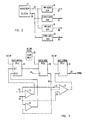
- Fig. 2 of the drawings shows a schematic diagram of a portion of the circuitry employed in the clock module 5.
- a master clock 11 which generates a series of pulses on two output lines, one designated as odd output line 13 and the other line 15 being designated as even output. Signals on these lines are at the same frequency and interleaved and comprise square wave pulses.
- the pulses on line 13 are supplied as inputs to an odd clock generator 17 and an odd gate generator 19, the outputs of which are designated by the references characters 0C and 0G respectively.
- the signals on line 15 shown on Fig. 2 are supplied to the inputs of an even clock generator 21 and an even gate generator 23, the outputs of which are designated as EC and EG respectively. It should be noted that more than one set of odd and even clock pulses and odd and even gate pulses may be generated in the master clock module 5. For example, in one proposed arrangement there will be five sets of odd and even clock and gate pulse pairs.
- the invention provides a verification of the reception of the gate signals and appropriate length thereof to assure proper generation of clocking signals internal to the receiving module 3.
- the arrangement will verify that all of the clock gate signals destined to the particular module are received and that they are not skewed to such an extreme where the clock time that is generated is chopped or generated as two short signals instead of a single clock signal. It will also detect an open or shortened condition on a gate input. This will verify the integrity of the clock signal at each receiving module, assuring that all modules 3 are synchronized in time relative to each other.
- Each of the clock distribution chips provided in each one of the modules 3 includes checking circuitry, one for each of the pairs of clock pulse and clock gates provided to the chip.
- the gate checking circuitry for each gate, consists of three polarity-hold latches and associated gate circuits. One such circuit is shown in Fig. 3 of the drawings.
- a scan-only latch 25 provides the ability to degate the checking arrangement.
- the primary function of this latch is to provide degate capability for unused gates which is required because, with multiple usage of the clock distribution chip, in many cases not all of the available gates are used.
- the secondary usage is to allow for maintaining the set condition of the gate arrival latch 27.
- the gate arrival latch 27 provides the ability to assure that the gate signal was present during a clock cycle. This function can be used as an initial test to assure that all gate signals expected are received. In normal operation it will be turned on at the active gate time and turned off after the data is transferred to the check gate latch.
- the check gate latch 29 opens a window or time period in which it is verified that the respective gate signal is not present at the next clock time. The gate signal must be present as an envelope only over the clock period following the clock time associated with the specific gate. As can be seen from the drawing, the output of the gate arrival latch 27 is supplied to the input of the check gate latch 29.
- the output of latch 29 is supplied as one input to an AND gate 31, the other inputs of which are the lines 33 and 35, carrying the even gate and even clock time signals from the lines EG and EC respectively.
- the output of check gate 29 is also supplied on its output line 30 to one input of an AND gate 37, the other input of which is connected to the even clock line EC.
- the output of AND gate 37 is supplied to the reset terminal of gate arrival latch 27.
- the set input of latch 27 is connected to the output of another AND circuit 39, the inputs of which are connected to the lines EG and EC as shown.
- the output of AND gate 31 is supplied to the gate error latch 41, which, when in its "on" state, provides an output signal on line 43 indicating an error in the timing and presence of the pulse and gate signals.
- the gate error latch will be turned on if, during the period of the check gate signal, the gate signal and its respective clock signal are present. This is a set only latch and once set will indicate the machine error on line 43, and it will be maintained in this condition until reset by machine check interrogation controls, not shown.
- the allow check scan-only latches will be turned off by suitable controls, not shown.
- the master clock 5 will then be run for one maximum length cycle, such for example as eight clock periods and thereafter the gate arrival latches 27 will be read to verify that all destined gate signals arrived at their destination.
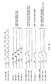
- Fig. 4 of the drawings illustrates the wave forms which are present at various locations in the circuitry shown in Fig. 3, and at different times and conditions of the system.
- Wave forms 51 and 53 show the sequence of pulses and their interleaved relation for the odd and even clock signals.
- the wave forms 55, 57, 59 and 61 are for even and odd gate signals 1, and even and odd gate signals 2 as designated in the drawing. This is representative of a single four- pulse clock cycle in which the gate signals have a normal skew as shown by the hatched portion.
- next wave form, 69 indicates an even gate 1 signal with an excessive skew.
- the gate arrival latch, the check gate latch and the gate error latch behave as indicated in wave form 71, 73 and 75. It will be noted that this combination of inputs will set gate error latch on and an output therefore will be provided on the line 43 of the circuitry shown on Fig. 3 to indicate that an excessive skew error has been detected.
- the present invention provides an arrangement for distribution of timing signals to a plurality of circuit modules contained within a digital system employing a centralized source or clock of synchronizing signals.
- the arrangement includes means for checking the proper sequence and timing of the arrival of the signals at the circuit modules where they are to be used.
Landscapes
- Engineering & Computer Science (AREA)
- Theoretical Computer Science (AREA)
- Physics & Mathematics (AREA)
- General Engineering & Computer Science (AREA)
- General Physics & Mathematics (AREA)
- Tests Of Electronic Circuits (AREA)
- Test And Diagnosis Of Digital Computers (AREA)
- Manipulation Of Pulses (AREA)
Claims (5)
Applications Claiming Priority (2)
| Application Number | Priority Date | Filing Date | Title |
|---|---|---|---|
| US06/342,270 US4482819A (en) | 1982-01-25 | 1982-01-25 | Data processor system clock checking system |
| US342270 | 1982-01-25 |
Publications (2)
| Publication Number | Publication Date |
|---|---|
| EP0085151A1 EP0085151A1 (fr) | 1983-08-10 |
| EP0085151B1 true EP0085151B1 (fr) | 1986-09-17 |
Family
ID=23341097
Family Applications (1)
| Application Number | Title | Priority Date | Filing Date |
|---|---|---|---|
| EP82111110A Expired EP0085151B1 (fr) | 1982-01-25 | 1982-12-02 | Système-rythmeur |
Country Status (4)
| Country | Link |
|---|---|
| US (1) | US4482819A (fr) |
| EP (1) | EP0085151B1 (fr) |
| JP (1) | JPS58129621A (fr) |
| DE (1) | DE3273382D1 (fr) |
Families Citing this family (7)
| Publication number | Priority date | Publication date | Assignee | Title |
|---|---|---|---|---|
| US4714924A (en) * | 1985-12-30 | 1987-12-22 | Eta Systems, Inc. | Electronic clock tuning system |
| US4851995A (en) * | 1987-06-19 | 1989-07-25 | International Business Machines Corporation | Programmable variable-cycle clock circuit for skew-tolerant array processor architecture |
| US4839907A (en) * | 1988-02-26 | 1989-06-13 | American Telephone And Telegraph Company, At&T Bell Laboratories | Clock skew correction arrangement |
| US5481573A (en) * | 1992-06-26 | 1996-01-02 | International Business Machines Corporation | Synchronous clock distribution system |
| TW418329B (en) * | 1994-08-24 | 2001-01-11 | Ibm | Integrated circuit clocking technique and circuit therefor |
| US5619158A (en) * | 1995-08-18 | 1997-04-08 | International Business Machines Corp. | Hierarchical clocking system using adaptive feedback |
| US10386912B2 (en) * | 2017-01-12 | 2019-08-20 | International Business Machines Corporation | Operating pulsed latches on a variable power supply |
Family Cites Families (6)
| Publication number | Priority date | Publication date | Assignee | Title |
|---|---|---|---|---|
| US3745472A (en) * | 1971-07-01 | 1973-07-10 | Texas Instruments Inc | Synchronous digital system having a clock distribution system |
| US3974333A (en) * | 1975-09-24 | 1976-08-10 | Bell Telephone Laboratories, Incorporated | Adaptive synchronization system |
| US4185245A (en) * | 1978-05-15 | 1980-01-22 | International Telephone And Telegraph Corporation | Fault-tolerant clock signal distribution arrangement |
| US4163946A (en) * | 1978-06-02 | 1979-08-07 | Gte Sylvania Incorporated | Noise-immune master timing generator |
| DE2853523C2 (de) * | 1978-12-12 | 1981-10-01 | Ibm Deutschland Gmbh, 7000 Stuttgart | Dezentrale Erzeugung von Taktsteuersignalen |
| DE2853546C2 (de) * | 1978-12-12 | 1982-02-25 | Ibm Deutschland Gmbh, 7000 Stuttgart | Prüfschaltung für mindestens zwei synchron arbeitende Taktgeber |
-
1982
- 1982-01-25 US US06/342,270 patent/US4482819A/en not_active Expired - Lifetime
- 1982-11-02 JP JP57192027A patent/JPS58129621A/ja active Granted
- 1982-12-02 EP EP82111110A patent/EP0085151B1/fr not_active Expired
- 1982-12-02 DE DE8282111110T patent/DE3273382D1/de not_active Expired
Non-Patent Citations (1)
| Title |
|---|
| None * |
Also Published As
| Publication number | Publication date |
|---|---|
| EP0085151A1 (fr) | 1983-08-10 |
| DE3273382D1 (en) | 1986-10-23 |
| JPS58129621A (ja) | 1983-08-02 |
| US4482819A (en) | 1984-11-13 |
| JPS6255166B2 (fr) | 1987-11-18 |
Similar Documents
| Publication | Publication Date | Title |
|---|---|---|
| US4630265A (en) | Method and apparatus for selecting for use between data buses in a redundant bus communication system | |
| US5349654A (en) | Fault tolerant data exchange unit | |
| US5537655A (en) | Synchronized fault tolerant reset | |
| EP0043432A2 (fr) | Dispositif pour la détection d'erreurs dans un système de transmission de données synchrones | |
| US4099668A (en) | Monitoring circuit | |
| EP0384177A2 (fr) | Synchronisation automatique à vernier de flux de données décalées | |
| KR890702124A (ko) | 디지탈 회로를 테스트하는 집적회로 애널라이저 | |
| KR950003948A (ko) | 다중 주파수출력 클럭 발생기 시스템 | |
| EP0085151B1 (fr) | Système-rythmeur | |
| US5381416A (en) | Detection of skew fault in a multiple clock system | |
| EP0434083A2 (fr) | Système et méthode de transmission de données | |
| US4229816A (en) | Timing signal generation and distribution system for TDM telecommunications systems | |
| CA1113575A (fr) | Circuit de verification pour horloges synchronisees | |
| US5528635A (en) | Synchronization detecting circuit | |
| US5627828A (en) | Method and circuit for detecting data collisions in communication network | |
| KR100370731B1 (ko) | 클럭선택기시스템 | |
| US4573171A (en) | Sync detect circuit | |
| US5764083A (en) | Pipelined clock distribution for self resetting CMOS circuits | |
| US6195769B1 (en) | Failsafe asynchronous data transfer corruption indicator | |
| US3903474A (en) | Periodic pulse check circuit | |
| US20030229836A1 (en) | Integrated circuit | |
| EP1482411B1 (fr) | Détection d'erreur dans un module de circuit | |
| US3265974A (en) | Signal detecting methods and devices | |
| US6157217A (en) | Method of synchronizing computing units connected to one another via a bus system | |
| US6272647B1 (en) | Fault tolerant clock voter with recovery |
Legal Events
| Date | Code | Title | Description |
|---|---|---|---|
| PUAI | Public reference made under article 153(3) epc to a published international application that has entered the european phase |
Free format text: ORIGINAL CODE: 0009012 |
|
| AK | Designated contracting states |
Designated state(s): DE FR GB |
|
| 17P | Request for examination filed |
Effective date: 19831122 |
|
| GRAA | (expected) grant |
Free format text: ORIGINAL CODE: 0009210 |
|
| AK | Designated contracting states |
Kind code of ref document: B1 Designated state(s): DE FR GB |
|
| REF | Corresponds to: |
Ref document number: 3273382 Country of ref document: DE Date of ref document: 19861023 |
|
| ET | Fr: translation filed | ||
| PLBE | No opposition filed within time limit |
Free format text: ORIGINAL CODE: 0009261 |
|
| STAA | Information on the status of an ep patent application or granted ep patent |
Free format text: STATUS: NO OPPOSITION FILED WITHIN TIME LIMIT |
|
| 26N | No opposition filed | ||
| PGFP | Annual fee paid to national office [announced via postgrant information from national office to epo] |
Ref country code: FR Payment date: 19951128 Year of fee payment: 14 |
|
| PGFP | Annual fee paid to national office [announced via postgrant information from national office to epo] |
Ref country code: DE Payment date: 19951229 Year of fee payment: 14 |
|
| PGFP | Annual fee paid to national office [announced via postgrant information from national office to epo] |
Ref country code: GB Payment date: 19961126 Year of fee payment: 15 |
|
| PG25 | Lapsed in a contracting state [announced via postgrant information from national office to epo] |
Ref country code: FR Effective date: 19970829 |
|
| PG25 | Lapsed in a contracting state [announced via postgrant information from national office to epo] |
Ref country code: DE Effective date: 19970902 |
|
| REG | Reference to a national code |
Ref country code: FR Ref legal event code: ST |
|
| PG25 | Lapsed in a contracting state [announced via postgrant information from national office to epo] |
Ref country code: GB Free format text: LAPSE BECAUSE OF NON-PAYMENT OF DUE FEES Effective date: 19971202 |
|
| GBPC | Gb: european patent ceased through non-payment of renewal fee |
Effective date: 19971202 |