EP0085219A2 - Gleichstrom-Gleichstromwandler mit einer Wechselstromverbindung - Google Patents
Gleichstrom-Gleichstromwandler mit einer Wechselstromverbindung Download PDFInfo
- Publication number
- EP0085219A2 EP0085219A2 EP82303075A EP82303075A EP0085219A2 EP 0085219 A2 EP0085219 A2 EP 0085219A2 EP 82303075 A EP82303075 A EP 82303075A EP 82303075 A EP82303075 A EP 82303075A EP 0085219 A2 EP0085219 A2 EP 0085219A2
- Authority
- EP
- European Patent Office
- Prior art keywords
- voltage
- type inverter
- terminals
- rectifiers
- controlled rectifiers
- Prior art date
- Legal status (The legal status is an assumption and is not a legal conclusion. Google has not performed a legal analysis and makes no representation as to the accuracy of the status listed.)
- Granted
Links
Images


Classifications
-
- H—ELECTRICITY
- H02—GENERATION; CONVERSION OR DISTRIBUTION OF ELECTRIC POWER
- H02M—APPARATUS FOR CONVERSION BETWEEN AC AND AC, BETWEEN AC AND DC, OR BETWEEN DC AND DC, AND FOR USE WITH MAINS OR SIMILAR POWER SUPPLY SYSTEMS; CONVERSION OF DC OR AC INPUT POWER INTO SURGE OUTPUT POWER; CONTROL OR REGULATION THEREOF
- H02M3/00—Conversion of DC power input into DC power output
- H02M3/22—Conversion of DC power input into DC power output with intermediate conversion into AC
- H02M3/24—Conversion of DC power input into DC power output with intermediate conversion into AC by static converters
- H02M3/28—Conversion of DC power input into DC power output with intermediate conversion into AC by static converters using discharge tubes with control electrode or semiconductor devices with control electrode to produce the intermediate AC
- H02M3/305—Conversion of DC power input into DC power output with intermediate conversion into AC by static converters using discharge tubes with control electrode or semiconductor devices with control electrode to produce the intermediate AC using devices of a thyratron or thyristor type requiring extinguishing means
- H02M3/315—Conversion of DC power input into DC power output with intermediate conversion into AC by static converters using discharge tubes with control electrode or semiconductor devices with control electrode to produce the intermediate AC using devices of a thyratron or thyristor type requiring extinguishing means using semiconductor devices only
Definitions
- the present invention relates to a DC-DC converter, more particularly to a DC-DC converter provided with a so called AC link, in which the controlled DC current is once converted into an AC current by using an inverter and which AC current is then converted back into a DC current again.
- a chopper type DC-DC converter incorporating a chopper circuit, which can produce a DC voltage higher than or lower than the input DC voltage.
- the former is known as the step-up chopper converter and the latter is known as the step-down chopper converter.
- Fig. la shows diagrammatically such a step-up type converter
- Fig. lb shows such a step-down type converter.
- 1 and 1' designate controlled rectifiers, which operate to close or open by an outer control signal.
- Example of these elements are transistors, gate turn-off (GTO) thyristors, and thyristors provided with a forced turn-off circuit.
- 2 and 2' are rectifiers
- 3 and 3' are DC smoothing-reactors
- 4 and 4' are DC smoothing capacitors
- P 1 and N 1 are the input terminals
- P 2 , N 2 , P 2 ' and N 2 ' are the output terminals.
- This converter is effective only for the step-up of the voltage.
- This converter is effective only for the step-down of the voltage. By this reason it has following features.
- FIG. 2 one example of a conventional DC-DC converter having inverter portions and provided with an AC link intermediary in which AC current flows, is shown in Fig. 2 and this embodiment will be explained hereinafter.
- Fig. 2 shows such a conventional DC-DC converter provided with an AC link.
- 11, 12, 13 and 14 are controlled rectifiers having the same function with the elements 1 and 1' shown in Figs. la and lb.
- 21, 22, 23, 24, 25, 26, 27 and 28 are rectifiers.
- 31 and 41 are the smoothing reactor and the smoothing capacitor.
- the circuit is divided into 2 parts which are coupled by a transformer 5.
- P 11 and N 11 designate DC input terminals
- AC I , AC 2 , AC 3 and AC4 are AC terminals
- P 21 and N 21 designate DC output terminals.
- a voltage type single phase bridge inverter is formed, which inverter controls the AC output voltage by pulse width modulation when the voltage is to be controlled.
- This AC output voltage is transformed by the transformer 5 and converted into a DC voltage by a rectifier circuit formed from rectifiers 25 to 28. Thereafter this output current is smoothed by the smoothing reactor 31 and the smoothing capacitor 41 and then fed to output P 21 and N 21 as a DC voltage.
- Such a conventional DC-DC converter provided with an AC link has the following advantages and disadvantages.
- the present invention had been obtained by studying the aforementioned various conventional systems.
- the present invention is to realize a novel DC-DC converter provided with an AC link, in which only the merits of the aforementioned various systems are incorporated.
- Fig. 3 shows the essential portion of the circuit diagram of one embodiment of the converter made according to the present invention.
- a single phase current type inverter is formed as shown on the left top side by a circuit including a smoothing reactor 31' and controlled rectifiers 11', 12', 13' and 14'. Further, a single phase half bridge voltage type inverter is formed as shown on the right side by controlled rectifiers 11" and 12", feedback rectifiers 21" and 22" (hereinafter called simply as rectifiers) connected in opposite parallel thereto, and smoothing capacitors 41' and 41" connected in series.
- the single phase current type inverter has the positive terminal P I and the negative terminal N I .
- the single phase half bridge voltage type inverter has the positive terminal P v and the negative terminal N V .
- the negative terminal N I of the former is connected in series with the positive terminal P V of the latter.
- AC terminals AC 1 ', AC 2 ', and ACg', AC 4 ' of these two inverters are coupled together through a transformer 6.
- the current type inverter and the voltage type inverter are both known per se so that a detailed explanation of their construction is omitted.
- the controlled rectifier elements (11'-14' 11", 12") may be the same elements as those shown in Figs. la, lb and 2.
- the AC output voltage e INV of the transformer 6 fed from the voltage type inverter is determinantly decided by the controlled rectifiers 11" and 12" and is a rectangular waveform having the wave height V D .
- This waveform is shown on the 5th line of Fig. 4.
- a rectangular waveform having the wave height nV D should be derived at the AC terminals AC 1 ', AC 2 ' of the current type inverter.
- the controlled rectifiers 11' and 14' are so adjusted as to turn on at a time advanced by a controlled angle y from a standard point at which the AC output voltage e INV changes its polarity from negative to positive.
- the controlled rectifiers 12' and 13' are so adjusted as to turn on at a time advanced by a controlled angle y from a standard point at which AC output voltage changes its polarity from positive to negative.
- the voltage 2V D namely the output DC voltage of the voltage type inverter forming the output of the DC-DC converter is determined by the control angle y. Therefore, it may be understood that by controlling this control angle y with respect to the variation of the input voltage E, the output voltage 2V D of the DC-DC converter can be made constant.
- the controlled rectifiers 11' and 14' As for the voltage of the controlled rectifiers 11' and 14', these rectifiers are turned on during the periods of PD 1 and PD 2 so that the voltage across these rectifiers assumes value zero. In a period of PD 3 , the controlled rectifiers 12' and 13' are turned on and by this a reverse voltage of (-nV D ) is applied to the rectifiers 11' and 14'. In the next period of PD 4 , by the reversing of polarity of the AC output voltage, a forward voltage of (+nV D ) is applied thereto. The same is applied to the controlled rectifiers 12' and 13' and the voltage is as shown on the next line.
- the reversed current can be controlled without providing a forced reverse current circuit portion even normal thyristors are used for the controlled rectifiers.
- E min is as follows.
- the input current is continuous and the ripple can be suppressed at a small value and an output power having the voltage stepped up or stepped down with respect to the input voltage can be obtained.
- the transformer can be minimized substantially.
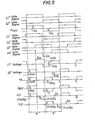
- the controlled rectifiers 11' and 13' are controlled with a fixed sufficiently small advanced control angle ⁇ 13 against the AC output voltage as shown in the diagram.
- the controlled rectifiers 12' and 14' are controlled at a large advanced angle Y24 with respect to the AC voltage.
- the advanced control angle y 13 is so arranged that during this period, by applying a reverse voltage to the controlled rectifiers 11' and 13', it is able to turn off these controlled rectifiers, in case the current type inverter is an AC line voltage commutation system.
- the relation between the input and output voltages is given by the following equation (6).
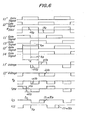
- the advanced control angle Y24 of the controlled rectifiers 12' and 14' is fixed at n, whereas the advanced control angle ⁇ 13 of the controlled rectifiers 11' and 13' is controlled.
- the waveforms for this case corresponding to Fig. 5 is shown in Fig. 6.
- the waveforms shown in Figs. 5 and 6 have the identical variation range for the input voltage with that shown in Fig. 4, but the difference is that the current flowing through the voltage type inverter winding 6b of the transformer 6 assumes value zero over a period in which both the pair of controlled rectifiers 11' and 12' and the pair of 13' and 14' are turned-on. This period corresponds to a condition that the DC voltage of the current type inverter is short circuited.
- the transformer 6 may be a short time rating one and thus a considerably small transformer can be used. Furthermore the current flowing through the voltage type inverter is also small, and this contributes to the miniaturization and the circuit loss is also kept small. Another merit is that the ripple voltage of the DC voltage V B of the current type inverter can be made small which further contributes for the miniaturization of the smoothing reactor 31' and other associated devices.
- the transformer and the reactors may further be reduced for the size.
- the abovementioned embodiment is a case that a half bridge is used for the voltage type inverter. But it is apparent that a single phase full bridge inverter can be applied therefor.
- the order of connection of DC terminals may be opposite from the case shown in the figure.
- the operation is entirely the same.
- the position of insertion of the smoothing reactor is not limited to a case shown in Fig. 3. It may be inserted at any portion in the series circuit portion.
- the present invention utilizes the various merits of conventional systems by combining a current type inverter and a voltage type inverter and a novel and useful converter system is realized.
Landscapes
- Engineering & Computer Science (AREA)
- Power Engineering (AREA)
- Rectifiers (AREA)
- Inverter Devices (AREA)
- Dc-Dc Converters (AREA)
Applications Claiming Priority (4)
| Application Number | Priority Date | Filing Date | Title |
|---|---|---|---|
| JP1168582A JPS58130774A (ja) | 1982-01-29 | 1982-01-29 | 直流直流変換制御方法 |
| JP11684/82 | 1982-01-29 | ||
| JP11685/82 | 1982-01-29 | ||
| JP1168482A JPS58130773A (ja) | 1982-01-29 | 1982-01-29 | Acリンク付dc−dcコンバ−タ |
Publications (3)
| Publication Number | Publication Date |
|---|---|
| EP0085219A2 true EP0085219A2 (de) | 1983-08-10 |
| EP0085219A3 EP0085219A3 (en) | 1984-02-22 |
| EP0085219B1 EP0085219B1 (de) | 1986-02-19 |
Family
ID=26347161
Family Applications (1)
| Application Number | Title | Priority Date | Filing Date |
|---|---|---|---|
| EP82303075A Expired EP0085219B1 (de) | 1982-01-29 | 1982-06-14 | Gleichstrom-Gleichstromwandler mit einer Wechselstromverbindung |
Country Status (4)
| Country | Link |
|---|---|
| US (1) | US4462070A (de) |
| EP (1) | EP0085219B1 (de) |
| DE (1) | DE3269150D1 (de) |
| FI (1) | FI822372L (de) |
Cited By (1)
| Publication number | Priority date | Publication date | Assignee | Title |
|---|---|---|---|---|
| WO2010055016A3 (de) * | 2008-11-12 | 2010-12-23 | Logicdata Electronic & Software Entwicklungs Gmbh | Steuerung für ein elektrisch verstellbares möbel |
Families Citing this family (7)
| Publication number | Priority date | Publication date | Assignee | Title |
|---|---|---|---|---|
| US5027264A (en) * | 1989-09-29 | 1991-06-25 | Wisconsin Alumni Research Foundation | Power conversion apparatus for DC/DC conversion using dual active bridges |
| CA2364416A1 (en) | 2000-12-18 | 2002-06-18 | Abb Industrie Ag | Converter system for increasing a dc voltage |
| US20060244460A1 (en) * | 2005-04-29 | 2006-11-02 | Weaver Jeffrey S | System and method for battery management |
| US7112937B1 (en) | 2005-10-31 | 2006-09-26 | Hewlett-Packard Development Company, Lp. | Device and method for driving a motor |
| US9166415B2 (en) * | 2005-11-24 | 2015-10-20 | Komatsu Ltd. | AC link bidirectional DC-DC converter, hybrid power supply system using the same and hybrid vehicle |
| WO2014071597A1 (en) * | 2012-11-09 | 2014-05-15 | Abb Technology Ltd. | A step-down dc autotransformer for hvdc and a system thereof |
| EP4236048B1 (de) | 2019-05-24 | 2026-05-20 | Huawei Digital Power Tech Co Ltd | Integriertes ladegerät und motorsteuerungssystem mit einem transformator und mehrstufigen stromrichtern |
Family Cites Families (4)
| Publication number | Priority date | Publication date | Assignee | Title |
|---|---|---|---|---|
| US3953779A (en) * | 1974-05-30 | 1976-04-27 | Francisc Carol Schwarz | Electronic control system for efficient transfer of power through resonant circuits |
| SE406530B (sv) * | 1977-06-27 | 1979-02-12 | Asea Ab | Likspenningsomriktare |
| EP0034075B1 (de) * | 1980-01-24 | 1984-04-18 | Merlin Gerin | Statische Stromversorgungsvorrichtung eines Elektrofilters für die elektrostatische Entstaubung |
| GB2087171A (en) * | 1980-11-05 | 1982-05-19 | Chloride Group Ltd | Static inverter |
-
1982
- 1982-06-10 US US06/386,942 patent/US4462070A/en not_active Expired - Lifetime
- 1982-06-14 DE DE8282303075T patent/DE3269150D1/de not_active Expired
- 1982-06-14 EP EP82303075A patent/EP0085219B1/de not_active Expired
- 1982-07-02 FI FI822372A patent/FI822372L/fi not_active Application Discontinuation
Cited By (2)
| Publication number | Priority date | Publication date | Assignee | Title |
|---|---|---|---|---|
| WO2010055016A3 (de) * | 2008-11-12 | 2010-12-23 | Logicdata Electronic & Software Entwicklungs Gmbh | Steuerung für ein elektrisch verstellbares möbel |
| US8638083B2 (en) | 2008-11-12 | 2014-01-28 | Logicdata Electronic & Software Entwicklungs Gmbh | Control for an electrically adjustable piece of furniture |
Also Published As
| Publication number | Publication date |
|---|---|
| FI822372A0 (fi) | 1982-07-02 |
| DE3269150D1 (en) | 1986-03-27 |
| FI822372A7 (fi) | 1983-07-30 |
| FI822372L (fi) | 1983-07-30 |
| US4462070A (en) | 1984-07-24 |
| EP0085219B1 (de) | 1986-02-19 |
| EP0085219A3 (en) | 1984-02-22 |
Similar Documents
| Publication | Publication Date | Title |
|---|---|---|
| US5483433A (en) | Voltage control circuit for a multiple stage DC power supply, and applications thereof | |
| US4833582A (en) | Frequency converter circuit including a single-ended blocking frequency converter | |
| US4502104A (en) | Bootstrapped AC-DC power converter | |
| EP0085219B1 (de) | Gleichstrom-Gleichstromwandler mit einer Wechselstromverbindung | |
| US4422139A (en) | Transformer coupled up-down converter | |
| EP0534422A2 (de) | Stromversorgungsvorrichtung | |
| JP3290746B2 (ja) | Dc/dcコンバータを含む低損失電源供給装置 | |
| US11637492B2 (en) | Buck matrix-type rectifier with boost switch, and operation thereof during one-phase loss | |
| JP3014649B2 (ja) | Dc/dcコンバータで構成される増設直流電源 | |
| JPH067743B2 (ja) | 電源装置 | |
| JPH10164832A (ja) | 直流昇降圧装置 | |
| JPH07222443A (ja) | Dc−dcコンバータ | |
| JPS5970147A (ja) | 昇降圧コンバ−タの並列動作方式 | |
| JPS6232707B2 (de) | ||
| JPS6232706B2 (de) | ||
| JPH0686539A (ja) | コンバータ回路 | |
| JPS6253171A (ja) | 車両用補助電源装置 | |
| US6777919B1 (en) | Switched power supply converter for broad range of input voltages | |
| JP2708861B2 (ja) | 電力変換装置 | |
| SU1457118A1 (ru) | Регулируемый источник тока | |
| SU760336A1 (ru) | Способ управления' регулятором напряжения 1 2 | |
| JP2003169473A (ja) | 直流電源装置 | |
| JPH0993930A (ja) | スイッチング電源装置およびその制御方法 | |
| JPH0496649A (ja) | スイッチングレギュレータ | |
| JPS6347072B2 (de) |
Legal Events
| Date | Code | Title | Description |
|---|---|---|---|
| PUAI | Public reference made under article 153(3) epc to a published international application that has entered the european phase |
Free format text: ORIGINAL CODE: 0009012 |
|
| AK | Designated contracting states |
Designated state(s): CH DE FR GB LI SE |
|
| PUAL | Search report despatched |
Free format text: ORIGINAL CODE: 0009013 |
|
| AK | Designated contracting states |
Designated state(s): CH DE FR GB LI SE |
|
| 17P | Request for examination filed |
Effective date: 19840307 |
|
| GRAA | (expected) grant |
Free format text: ORIGINAL CODE: 0009210 |
|
| AK | Designated contracting states |
Designated state(s): CH DE FR GB LI SE |
|
| REF | Corresponds to: |
Ref document number: 3269150 Country of ref document: DE Date of ref document: 19860327 |
|
| ET | Fr: translation filed | ||
| PLBE | No opposition filed within time limit |
Free format text: ORIGINAL CODE: 0009261 |
|
| STAA | Information on the status of an ep patent application or granted ep patent |
Free format text: STATUS: NO OPPOSITION FILED WITHIN TIME LIMIT |
|
| 26N | No opposition filed | ||
| EAL | Se: european patent in force in sweden |
Ref document number: 82303075.4 |
|
| PGFP | Annual fee paid to national office [announced via postgrant information from national office to epo] |
Ref country code: FR Payment date: 19960515 Year of fee payment: 15 |
|
| PGFP | Annual fee paid to national office [announced via postgrant information from national office to epo] |
Ref country code: SE Payment date: 19960529 Year of fee payment: 15 |
|
| PGFP | Annual fee paid to national office [announced via postgrant information from national office to epo] |
Ref country code: GB Payment date: 19960606 Year of fee payment: 15 |
|
| PGFP | Annual fee paid to national office [announced via postgrant information from national office to epo] |
Ref country code: CH Payment date: 19960626 Year of fee payment: 15 |
|
| PGFP | Annual fee paid to national office [announced via postgrant information from national office to epo] |
Ref country code: DE Payment date: 19960731 Year of fee payment: 15 |
|
| PG25 | Lapsed in a contracting state [announced via postgrant information from national office to epo] |
Ref country code: GB Free format text: LAPSE BECAUSE OF NON-PAYMENT OF DUE FEES Effective date: 19970614 |
|
| PG25 | Lapsed in a contracting state [announced via postgrant information from national office to epo] |
Ref country code: SE Effective date: 19970615 |
|
| PG25 | Lapsed in a contracting state [announced via postgrant information from national office to epo] |
Ref country code: LI Free format text: LAPSE BECAUSE OF NON-PAYMENT OF DUE FEES Effective date: 19970630 Ref country code: CH Free format text: LAPSE BECAUSE OF NON-PAYMENT OF DUE FEES Effective date: 19970630 |
|
| GBPC | Gb: european patent ceased through non-payment of renewal fee |
Effective date: 19970614 |
|
| REG | Reference to a national code |
Ref country code: CH Ref legal event code: PL |
|
| PG25 | Lapsed in a contracting state [announced via postgrant information from national office to epo] |
Ref country code: FR Free format text: LAPSE BECAUSE OF NON-PAYMENT OF DUE FEES Effective date: 19980227 |
|
| EUG | Se: european patent has lapsed |
Ref document number: 82303075.4 |
|
| PG25 | Lapsed in a contracting state [announced via postgrant information from national office to epo] |
Ref country code: DE Free format text: LAPSE BECAUSE OF NON-PAYMENT OF DUE FEES Effective date: 19980303 |
|
| REG | Reference to a national code |
Ref country code: FR Ref legal event code: ST |
|
| REG | Reference to a national code |
Ref country code: FR Ref legal event code: ST |