EP0085241A2 - Oscillateur à configuration commutable - Google Patents
Oscillateur à configuration commutable Download PDFInfo
- Publication number
- EP0085241A2 EP0085241A2 EP82306666A EP82306666A EP0085241A2 EP 0085241 A2 EP0085241 A2 EP 0085241A2 EP 82306666 A EP82306666 A EP 82306666A EP 82306666 A EP82306666 A EP 82306666A EP 0085241 A2 EP0085241 A2 EP 0085241A2
- Authority
- EP
- European Patent Office
- Prior art keywords
- oscillator
- transistors
- gates
- gate
- frequency
- Prior art date
- Legal status (The legal status is an assumption and is not a legal conclusion. Google has not performed a legal analysis and makes no representation as to the accuracy of the status listed.)
- Granted
Links
Images




Classifications
-
- H—ELECTRICITY
- H03—ELECTRONIC CIRCUITRY
- H03B—GENERATION OF OSCILLATIONS, DIRECTLY OR BY FREQUENCY-CHANGING, BY CIRCUITS EMPLOYING ACTIVE ELEMENTS WHICH OPERATE IN A NON-SWITCHING MANNER; GENERATION OF NOISE BY SUCH CIRCUITS
- H03B5/00—Generation of oscillations using amplifier with regenerative feedback from output to input
- H03B5/18—Generation of oscillations using amplifier with regenerative feedback from output to input with frequency-determining element comprising distributed inductance and capacitance
- H03B5/1841—Generation of oscillations using amplifier with regenerative feedback from output to input with frequency-determining element comprising distributed inductance and capacitance the frequency-determining element being a strip line resonator
- H03B5/1847—Generation of oscillations using amplifier with regenerative feedback from output to input with frequency-determining element comprising distributed inductance and capacitance the frequency-determining element being a strip line resonator the active element in the amplifier being a semiconductor device
- H03B5/1852—Generation of oscillations using amplifier with regenerative feedback from output to input with frequency-determining element comprising distributed inductance and capacitance the frequency-determining element being a strip line resonator the active element in the amplifier being a semiconductor device the semiconductor device being a field-effect device
-
- H—ELECTRICITY
- H03—ELECTRONIC CIRCUITRY
- H03B—GENERATION OF OSCILLATIONS, DIRECTLY OR BY FREQUENCY-CHANGING, BY CIRCUITS EMPLOYING ACTIVE ELEMENTS WHICH OPERATE IN A NON-SWITCHING MANNER; GENERATION OF NOISE BY SUCH CIRCUITS
- H03B2200/00—Indexing scheme relating to details of oscillators covered by H03B
- H03B2200/003—Circuit elements of oscillators
- H03B2200/0048—Circuit elements of oscillators including measures to switch the frequency band, e.g. by harmonic selection
-
- H—ELECTRICITY
- H03—ELECTRONIC CIRCUITRY
- H03B—GENERATION OF OSCILLATIONS, DIRECTLY OR BY FREQUENCY-CHANGING, BY CIRCUITS EMPLOYING ACTIVE ELEMENTS WHICH OPERATE IN A NON-SWITCHING MANNER; GENERATION OF NOISE BY SUCH CIRCUITS
- H03B2200/00—Indexing scheme relating to details of oscillators covered by H03B
- H03B2200/006—Functional aspects of oscillators
- H03B2200/0098—Functional aspects of oscillators having a balanced output signal
Definitions
- the present invention relates to a multi-band microwave oscillator.
- a general difficulty in adapting microwave techniques for consumer and commercial applications is the difficulty of fabricating cheap structures which are not confined to a relatively narrow bandwidth.
- satellite down links and assigned satellite broadcast bands are widely spaced across the microwave spectrum, and it is difficult enough to design a receiver to cover much bf any one band, without attempting to cover multiple bands.
- the ability to select among channels of reception is highly desirable, not only to permit user versatility, but also to allow for adaptation to changing weather conditions, which may affect the propagation characteristics of different frequency bands differently.
- Multi-band capability in a local oscillator would permit multi-band reception in a conventional superheterodyne receiver, but there is at present no cheap way to achieve such multi-frequency capability in a single microwave local oscillator.
- Frequency-agility is useful in frequency-hopping communications systems. Such systems has been proposed to obtain better spectrum utilization where many users each have a low individual use rate and independent access as with mobile radio networks. Frequency-hopping agility is also useful in many military applications, particularly electronic countermeasures.
- the present invention provides an oscillator circuit incorporating transistors which are RF coupled but DC isolated.
- the gate of only one transistor is selectably biased into cut-off, converting the circuit from a two-active-element configuration into a one-active-element configuration.
- the circuit' is configured so that, when both devices are active, the circuit operates in the push-push mode. By this means a nearly two:one ratio of oscillation frequencies is obtained.
- a switched-geometry network incorporates more than two active elements to permit selection of more than two frequencies.
- the switched-geometry oscillator switches the local-oscillator frequency between two different bands, permitting multi-band microwave reception.
- plural switched-geometry oscillators are used by using additional switched-geometry oscillators to selectively alter the downconversion to the lower intermediate frequencies.
- Figure 1 shows generally a first configuration of the switched-geometry oscillator of the present invention. Note that the gates of FET 1 and FET 2 are DC-isolated by capacitor 12, but this capacitor does not interfere with the RF connection at microwave frequencies.
- a bias circuit connected through radio frequency choke 14 and grounding capacitor 16, provides the bias voltage from terminal V switch to FET 1 only. By providing a sufficiently large bias voltage at terminal V sw it ch , FET 1 may be kept pinched off through the complete RF cycle of the circuit. Thus, the effect of applying different bias voltages is to change the effective circuit configuration between the two states shown in Figures and 2b.
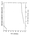
- Figure 2a shows the effective configuration of the circuit where both devices are active. In the configuration as shown, this will normally result in push-push operation, as shown in Figure 3, where each device oscillates at half of the circuit output frequency, but the asymmetrical output currents generated by each separate device combine to produce a doubled output frequency in which the subharmonic (i.e. the frequency of each active device) is well suppressed.
- the RF voltage swing which is of opposite polarity at each gate, forward biases one FET's gate-source diode while pinching off the 2nd FET, and then reverses the process as the RF swing reverses.
- FET #1 As the gate of FET #1 is driven into forward diode conduction (clamping the gate-source voltage at .6 V) FET #2 is driven towards pinch-off. Since both gates are operated floating (no DC return) the RF swing centers on the zero voltage reference line. At zero volts on both FETs the total drain current is two times the IDSS current of a single FET. As one FET is driven towards pinch-off due to the RF voltage swing, the total drain current drops to IDSS of one device. This will effectively generate the second harmonic of the fundamental operating frequency of each FET as shown graphically in Figure 3A in the drain current plot.
- the sample embodiment of Figure 5 uses a two-section 50 to 15 ohm impedance transformer centered at 19 GHz and realized on 10 mil alumina.
- the two 300 gm FET's are alloyed to a 50 mil x 100 mil alumina circuit chip which was metallized on both sides.
- a 30 pF MIS capacitor was placed on the alumina chip beside the FETs as shown in Figure 5, and used to RF couple the gates.
- the second FET gate DC bias was taken out using a bond wire to a 30 pF capacitor as an RF choke.
- An external bias tee was used to handle the drain bias.
- the elements in the circuit design which determine whether the circuit will operate between push-push and fundamental modes, rather than between fundamental and fundmental times N (where N is greater than unity and is determined by the change in effective active capacitance plus the parasitic elements of the second pinched-off FET) are the placement of the inductance in the gate circuit.
- the DC blocking capacitor is transparent to RF, and inductive gate reactance is required to have oscillations in either the push-push or fundamental mode.
- the gate leads of FET 1 and FET 2 are separated by an inductive reactance (the capacitor is transparent to RF). This inductive reactance causes the phase difference between the gates which is necessary for push-push operation.
- Figure 7 shows a sample integrable embodiment of the oscillator of the present invention.
- metallization 22 is used for the drain of both FET 1 and FET 2.
- a source air bridge 24 is used to join the source areas of both FET 1 and of FET 2.
- the gate 26 of FET 1 is connected to a gate pad 28, and the gate 30 of FET 2 is connected to a gate pad 32.
- a MIM capacitor 34 is used to provide DC isolation between the gates.
- the relatively long and thin metal connector 36 provides additional resistance and inductance to isolate the DC gate pads -28 and 32 from the gates 26 and 30 respectively.
- the channel regions can be 75 microns wide, for a total gate length of 300 microns for each transistor.
- FIG 8 shows an example of how this switched-geometry oscillator might be combined with a tuning varactor 38, to provide an oscillator which could be both switched between different bands and tuned within each band.
- the tuning varactor 38 is connected to the RF gate pad 44.
- the use of separate gate bias connections 40 and 42, respectively indirectly connected to gate pads 28 and 32, permits optimization of frequency of operation, output power, and stable operating point of the FET. greater frequency agility is also obtained without the self-biasing gate.
- Conventional source networks 46, and a microwave impedance transformer 48 at the output are also provided according to techniques well known in the art.
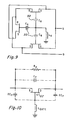
- Figure 9 shows an example of an embodiment which switches between fundamental-mode operation at two separate frequencies, and also an embodiment which uses more than two active devices.
- the limit on the number of devices which can be used in a switched-geometry oscillator according to the present invention' is in practice defined by how large the parasitic capacitance and resistance of the pinched-off devices is with respect to the gain and phase of the remaining active, devices.
- the gate-blocking capacitors 50 are preferably built monolithically, so that the inductive regenerative feedback (shown as element Lg in Figure 9) is common to the three gates at a well defined point, instead of having different phases at the three devices. If two devices are on and the third pinched off, then an equivalent circuit is as shown in Figure 10. Since the remaining active FETs are now operating in phase, they are shown as one combined equivalent element 52 in Figure 1 0 .
- the parasitic capacitances Cp of the pinched off FE T have small values, and the drain-source resistance R p of the pinched off FET is approximately five to ten times'higher than the series resistance of an active FET, a relatively small amount of feedback is generated.
- the crucial limitation here is that a sufficient feedback path will reduce the gain of the equivalent active element 52 below that which will sustain oscillations. Note that increasing the bias voltage to the pinched-off FETs beyond that necessary to cause pinch off will reduce the parasitic capacitance C p and increase the parasitic resistance R p, permitting a larger number of FETs in a multi-FET oscillator to be pinched off.
- the pinched-off FET provides both parasitic capacitance and parasitic resistance.
- the parasitic reactance provides a fine tuning of the desired oscillatory frequency of the remaining active device. Biasing beyond pinch-off will greatly reduce the parasitic resistance, but excessive biasing also reduces the parasitic capacitance.
- excessive bias beyond the point where pinch-off occurs can be used to fine tune the desired frequency shift, and at least some bias beyond pinch-off is desirable to control parasitic resistance.
- Figure 1 has been shown with self-biasing gates, as disclosed and claimed in U .S. Patent Application No. 292,769, filed August 14, 1981, which is hereby incorporated by reference.
- the use of the floating gate for the device that will always remain active could simplifiy the layout and reduce parasitic elements in multiple FET designs, since it would not require the extra pads and RF choke to get the DC bias into the device.
- the gate lengths of the devices used need not be equal.
- three oscillating frequencies are selectively attained where the two devices have different gate lengths, according to whether the shorter, the longer, or neither is pinched off. (Of course, each transistor must have a separate gate bias circuit since any one transistor may be pinched-off.)
- the number of available frequencies in a multiple-device circuit may be increased by using dissimilar devices.
- the set of active gate lengths which can be used is limited by the ratio of voltage gain per unit gate length of active device to voltage loss (into parasitic resistance) per unit gate length of pinched-off device.
- a gain/loss ratio of around 10:1 is easily attainable.
- a three-device circuit having gate lengths in the ratio of 1:2:4 permits any one active device to sustain oscillation, and numerous distinct oscillatory frequencies can be selected.
- more than one switched-geometry oscillator may be used to further increase the number of available frequencies. For example, if the downconversion from the first intermediate frequency to the next lower intermediate frequency is accomplished by means of a switched-geometry oscillator, more than one first: intermediate frequency may selectively be used.
- a switched geometry oscillator provided at the local oscillator stage can switch between 10 GHz and 15 GHz
- a switched-geometry oscillator is provided to down convert from the first intermediate frequency which can switch between 1 GHz and 1.5 GHz
- the second intermediate frequency is 100 Megahertz
- a dielectric resonator structure can be used (in a reflective, transmissive, or reactive configuration) with the switched-geometry oscillator to obtain stabilized oscillations at each frequency.
- Dielectric resonator structures are well known to have multiple modes at widely spaced frequencies which differ in insertion loss by only a few decibels. These parameters (insertion loss, fundamental and other mode frequencies) are affected by the dielectric constant, width to height ratio, and shape of the structure (circle, rectangle, etc.) and therefore are selectible to match those required for stabilization of a switched-geometry oscillator. Further background on dielectric resonators is found in IEEE Trans. Microwave Theory Tech., Vol. MTT-29, pp.
- each resonator is alternatively stabilizing the oscillator at one frequency but becomes transparent at all other frequencies.
- GaAs MESFET permits an easy solution to the unique problems of microwave systems as discussed above.
- the invention is realized using N-channel MESFET devices having about .5 micron channel length (ca..4 micron gate length), formed in an epitaxial or implanted device layer on a semi-insulating GaAs substrate. (As discussed above, the gate width is typically hundreds of microns.)
- the switched-geometry oscillator is preferably integrated with one or more monolithic varactors as disclosed in U.S. Patent Application Serial Nos. 292,770 and 293,040, both filed August 14, 1981, which are both hereby incorporated by reference, to provide fine-tuning.
Landscapes
- Inductance-Capacitance Distribution Constants And Capacitance-Resistance Oscillators (AREA)
- Superheterodyne Receivers (AREA)
Applications Claiming Priority (2)
| Application Number | Priority Date | Filing Date | Title |
|---|---|---|---|
| US345265 | 1982-02-02 | ||
| US06/345,265 US4485355A (en) | 1982-02-02 | 1982-02-02 | Switched geometry oscillator |
Publications (3)
| Publication Number | Publication Date |
|---|---|
| EP0085241A2 true EP0085241A2 (fr) | 1983-08-10 |
| EP0085241A3 EP0085241A3 (en) | 1983-08-24 |
| EP0085241B1 EP0085241B1 (fr) | 1986-02-26 |
Family
ID=23354282
Family Applications (1)
| Application Number | Title | Priority Date | Filing Date |
|---|---|---|---|
| EP82306666A Expired EP0085241B1 (fr) | 1982-02-02 | 1982-12-14 | Oscillateur à configuration commutable |
Country Status (4)
| Country | Link |
|---|---|
| US (1) | US4485355A (fr) |
| EP (1) | EP0085241B1 (fr) |
| JP (1) | JPS58134514A (fr) |
| DE (1) | DE3269520D1 (fr) |
Cited By (5)
| Publication number | Priority date | Publication date | Assignee | Title |
|---|---|---|---|---|
| FR2559626A1 (fr) * | 1984-02-14 | 1985-08-16 | Thomson Csf | Oscillateur haute frequence commande en tension |
| EP0242292A1 (fr) * | 1986-04-18 | 1987-10-21 | Thomson-Csf | Oscillateur commandé par une tension, doubleur de fréquence |
| EP0465314A1 (fr) * | 1990-07-04 | 1992-01-08 | Matra Communication | Amplificateur à sortie en double bande |
| EP0527470A1 (fr) * | 1991-08-12 | 1993-02-17 | Matsushita Electric Industrial Co., Ltd. | Oscillateur push-push |
| EP0718964A3 (fr) * | 1994-12-20 | 1996-10-02 | Fujitsu Compound Semiconductor | Circuit oscillateur commutable et procédé |
Families Citing this family (17)
| Publication number | Priority date | Publication date | Assignee | Title |
|---|---|---|---|---|
| FR2561048B1 (fr) * | 1984-03-09 | 1986-09-19 | Thomson Csf | Oscillateur hyperfrequences a transistor, commande par capacite variable |
| US4620143A (en) * | 1984-11-09 | 1986-10-28 | Westinghouse Electric Corp. | Digital pulse width modulation motor control system |
| US4677691A (en) * | 1985-08-01 | 1987-06-30 | Texas Instruments Incorporated | Microwave receiver |
| GB2181914B (en) * | 1985-10-22 | 1989-09-20 | Plessey Co Plc | Frequency doubling oscillator and heterodyne circuit incorporating same |
| US4763084A (en) * | 1986-05-27 | 1988-08-09 | Texas Instruments Incorporated | Push-push dielectric resonator oscillator |
| FR2600215B1 (fr) * | 1986-06-13 | 1988-08-19 | Thomson Csf | Oscillateur doubleur de frequence, fonctionnant en hyperfrequences |
| DE3709357A1 (de) * | 1987-03-21 | 1988-09-29 | Philips Patentverwaltung | Mikrowellen-oszillator |
| DE3709356A1 (de) * | 1987-03-21 | 1988-09-29 | Philips Patentverwaltung | Mikrowellen-oszillator |
| US5231361A (en) * | 1990-02-05 | 1993-07-27 | Trw Inc. | Voltage controlled push-push oscillator with parallel resonant tank circuits |
| JP2910421B2 (ja) * | 1991-09-17 | 1999-06-23 | 日本電気株式会社 | マイクロ波発振器 |
| US5402087A (en) * | 1994-04-08 | 1995-03-28 | B.E.L.-Tronics Limited | Voltage controlled push-push oscillator |
| DE19709289A1 (de) * | 1997-03-07 | 1998-09-10 | Thomson Brandt Gmbh | Schaltung zur Vermeidung von parasitären Schwingmodi in einem Oszillator Schwingkreis |
| EP0863605B1 (fr) | 1997-03-07 | 2004-04-28 | Deutsche Thomson-Brandt Gmbh | Agencement de circuit pour éviter des modes d'oscillations parasitaires dans un circuit oscillateur |
| US5821820A (en) * | 1997-10-15 | 1998-10-13 | Motorola Inc. | Dual band voltage controlled oscillator |
| DE102006007380B4 (de) * | 2005-12-07 | 2017-12-14 | René Zimmer | Hochfrequenzgenerator, Hochfrequenzsender und deren Verwendung, insbesondere zur Erzeugung von UWB-Signalen |
| US7489207B1 (en) | 2008-04-22 | 2009-02-10 | International Business Machines Corporation | Structure for voltage controlled oscillator |
| US8970310B2 (en) * | 2012-10-10 | 2015-03-03 | Analog Devices, Inc. | Monolithic band switched coupled push-push oscillator |
Family Cites Families (5)
| Publication number | Priority date | Publication date | Assignee | Title |
|---|---|---|---|---|
| US3315178A (en) * | 1964-11-16 | 1967-04-18 | Doall Science Ct Inc | Transistor oscillator for extended frequency operation |
| US3328720A (en) * | 1965-07-15 | 1967-06-27 | Westinghouse Electric Corp | Dual mode oscillator circuits |
| ES359059A1 (es) * | 1968-10-11 | 1970-05-16 | Fagor Electrotecnica Sci | Sintonizador integrado electronicamente para t. v. |
| DE2263137B2 (de) * | 1972-12-22 | 1975-05-15 | Hans Kolbe & Co, 3202 Bad Salzdetfurth | Einrichtung zur Umsetzung sehr hoher Frequenzen |
| DE2334570B1 (de) * | 1973-07-07 | 1975-03-06 | Philips Patentverwaltung | Abstimmbare Hochfrequenz-Eingangsschaltungsanordnung fuer einen Fernsehempfaenger |
-
1982
- 1982-02-02 US US06/345,265 patent/US4485355A/en not_active Expired - Fee Related
- 1982-12-14 DE DE8282306666T patent/DE3269520D1/de not_active Expired
- 1982-12-14 EP EP82306666A patent/EP0085241B1/fr not_active Expired
-
1983
- 1983-02-01 JP JP58015363A patent/JPS58134514A/ja active Granted
Cited By (9)
| Publication number | Priority date | Publication date | Assignee | Title |
|---|---|---|---|---|
| FR2559626A1 (fr) * | 1984-02-14 | 1985-08-16 | Thomson Csf | Oscillateur haute frequence commande en tension |
| EP0242292A1 (fr) * | 1986-04-18 | 1987-10-21 | Thomson-Csf | Oscillateur commandé par une tension, doubleur de fréquence |
| FR2597678A1 (fr) * | 1986-04-18 | 1987-10-23 | Thomson Csf | Oscillateur commande par une tension, doubleur de frequence. |
| US4754236A (en) * | 1986-04-18 | 1988-06-28 | Thomson-Csf | Frequency-doubling voltage-controlled oscillator |
| EP0465314A1 (fr) * | 1990-07-04 | 1992-01-08 | Matra Communication | Amplificateur à sortie en double bande |
| FR2664444A1 (fr) * | 1990-07-04 | 1992-01-10 | Matra Communication | Amplificateur a sortie en double bande. |
| EP0527470A1 (fr) * | 1991-08-12 | 1993-02-17 | Matsushita Electric Industrial Co., Ltd. | Oscillateur push-push |
| US5250910A (en) * | 1991-08-12 | 1993-10-05 | Matsushita Electric Industrial Co., Ltd. | Push-push oscillator having in-phase and anti-phase output combining circuits |
| EP0718964A3 (fr) * | 1994-12-20 | 1996-10-02 | Fujitsu Compound Semiconductor | Circuit oscillateur commutable et procédé |
Also Published As
| Publication number | Publication date |
|---|---|
| JPS58134514A (ja) | 1983-08-10 |
| DE3269520D1 (en) | 1986-04-03 |
| EP0085241A3 (en) | 1983-08-24 |
| US4485355A (en) | 1984-11-27 |
| EP0085241B1 (fr) | 1986-02-26 |
| JPH0462202B2 (fr) | 1992-10-05 |
Similar Documents
| Publication | Publication Date | Title |
|---|---|---|
| US4485355A (en) | Switched geometry oscillator | |
| US6100770A (en) | MIS transistor varactor device and oscillator using same | |
| US11025198B2 (en) | Radio frequency oscillator | |
| US8957738B1 (en) | Voltage controlled oscillator | |
| US5345194A (en) | FET having two gate bonding pads for use in high frequency oscillator | |
| US6661301B2 (en) | Oscillator circuit | |
| US6107893A (en) | Voltage tunable active inductorless oscillator | |
| US6249191B1 (en) | Monolithic integrated circuit oscillators, complementary metal oxide semiconductor (CMOS) voltage-controlled oscillators, integrated circuit oscillators, oscillator-forming methods, and oscillation methods | |
| EP1563599B1 (fr) | Topologie d'oscillateur pour operation a tres faible bruit de phase | |
| Piernas et al. | A compact and low-phase-noise Ka-band pHEMT-based VCO | |
| US8102218B2 (en) | Parallel-structured switched variable inductor circuit | |
| US4754236A (en) | Frequency-doubling voltage-controlled oscillator | |
| KR960009970B1 (ko) | 트랙킹 특성이 개선된 동조 장치 | |
| US4189688A (en) | Microwave FET power oscillator | |
| KR960003664B1 (ko) | 이중 게이트 튜너블 발진기 | |
| US6842081B2 (en) | Dual frequency voltage controlled oscillator circuit | |
| EP0270298B1 (fr) | Oscillateur à large bande de réglage | |
| US4554516A (en) | Frequency source having YIG absorption/transmission filter | |
| US20020093388A1 (en) | Voltage-controlled oscillator and communication device | |
| US5159346A (en) | Voltage controlled oscillator | |
| US8547181B2 (en) | Oscillator with ohmically adjustable oscillation frequency | |
| EP1111771A2 (fr) | Oscillateur commande en tension utilisé en deux gammes de fréquence | |
| US9263987B2 (en) | Oscillator circuit | |
| Haddad et al. | A CMOS Digitally Controlled Oscillator for Reconfigurable RF Applications | |
| JPH104315A (ja) | 高周波発振回路 |
Legal Events
| Date | Code | Title | Description |
|---|---|---|---|
| PUAI | Public reference made under article 153(3) epc to a published international application that has entered the european phase |
Free format text: ORIGINAL CODE: 0009012 |
|
| PUAL | Search report despatched |
Free format text: ORIGINAL CODE: 0009013 |
|
| AK | Designated contracting states |
Designated state(s): DE FR GB IT NL |
|
| AK | Designated contracting states |
Designated state(s): DE FR GB IT NL |
|
| 17P | Request for examination filed |
Effective date: 19831005 |
|
| GRAA | (expected) grant |
Free format text: ORIGINAL CODE: 0009210 |
|
| AK | Designated contracting states |
Designated state(s): DE FR GB IT NL |
|
| PG25 | Lapsed in a contracting state [announced via postgrant information from national office to epo] |
Ref country code: NL Effective date: 19860226 Ref country code: IT Free format text: LAPSE BECAUSE OF FAILURE TO SUBMIT A TRANSLATION OF THE DESCRIPTION OR TO PAY THE FEE WITHIN THE PRESCRIBED TIME-LIMIT;WARNING: LAPSES OF ITALIAN PATENTS WITH EFFECTIVE DATE BEFORE 2007 MAY HAVE OCCURRED AT ANY TIME BEFORE 2007. THE CORRECT EFFECTIVE DATE MAY BE DIFFERENT FROM THE ONE RECORDED. Effective date: 19860226 |
|
| REF | Corresponds to: |
Ref document number: 3269520 Country of ref document: DE Date of ref document: 19860403 |
|
| ET | Fr: translation filed | ||
| NLV1 | Nl: lapsed or annulled due to failure to fulfill the requirements of art. 29p and 29m of the patents act | ||
| PLBE | No opposition filed within time limit |
Free format text: ORIGINAL CODE: 0009261 |
|
| STAA | Information on the status of an ep patent application or granted ep patent |
Free format text: STATUS: NO OPPOSITION FILED WITHIN TIME LIMIT |
|
| 26N | No opposition filed | ||
| PGFP | Annual fee paid to national office [announced via postgrant information from national office to epo] |
Ref country code: GB Payment date: 20011102 Year of fee payment: 20 |
|
| PGFP | Annual fee paid to national office [announced via postgrant information from national office to epo] |
Ref country code: FR Payment date: 20011203 Year of fee payment: 20 |
|
| PGFP | Annual fee paid to national office [announced via postgrant information from national office to epo] |
Ref country code: DE Payment date: 20011228 Year of fee payment: 20 |
|
| REG | Reference to a national code |
Ref country code: GB Ref legal event code: IF02 |
|
| PG25 | Lapsed in a contracting state [announced via postgrant information from national office to epo] |
Ref country code: GB Free format text: LAPSE BECAUSE OF EXPIRATION OF PROTECTION Effective date: 20021213 |
|
| REG | Reference to a national code |
Ref country code: GB Ref legal event code: PE20 Effective date: 20021213 |