EP0085260A2 - Circuit de mémoire non-volatile à semi-conducteurs - Google Patents
Circuit de mémoire non-volatile à semi-conducteurs Download PDFInfo
- Publication number
- EP0085260A2 EP0085260A2 EP82306993A EP82306993A EP0085260A2 EP 0085260 A2 EP0085260 A2 EP 0085260A2 EP 82306993 A EP82306993 A EP 82306993A EP 82306993 A EP82306993 A EP 82306993A EP 0085260 A2 EP0085260 A2 EP 0085260A2
- Authority
- EP
- European Patent Office
- Prior art keywords
- type transistor
- depletion
- transistor
- nonvolatile semiconductor
- semiconductor memory
- Prior art date
- Legal status (The legal status is an assumption and is not a legal conclusion. Google has not performed a legal analysis and makes no representation as to the accuracy of the status listed.)
- Granted
Links
Images


Classifications
-
- G—PHYSICS
- G11—INFORMATION STORAGE
- G11C—STATIC STORES
- G11C16/00—Erasable programmable read-only memories
- G11C16/02—Erasable programmable read-only memories electrically programmable
- G11C16/06—Auxiliary circuits, e.g. for writing into memory
- G11C16/26—Sensing or reading circuits; Data output circuits
- G11C16/28—Sensing or reading circuits; Data output circuits using differential sensing or reference cells, e.g. dummy cells
-
- G—PHYSICS
- G11—INFORMATION STORAGE
- G11C—STATIC STORES
- G11C16/00—Erasable programmable read-only memories
- G11C16/02—Erasable programmable read-only memories electrically programmable
- G11C16/04—Erasable programmable read-only memories electrically programmable using variable threshold transistors, e.g. FAMOS
- G11C16/0408—Erasable programmable read-only memories electrically programmable using variable threshold transistors, e.g. FAMOS comprising cells containing floating gate transistors
- G11C16/0433—Erasable programmable read-only memories electrically programmable using variable threshold transistors, e.g. FAMOS comprising cells containing floating gate transistors comprising cells containing a single floating gate transistor and one or more separate select transistors
Definitions
- nonvolatile semiconductor memory circuits which electrically write or erase information have frequently been used since in these circuits it is unnecessary to use an ultraviolet ray, etc., the use of which is a drawback.
- the principle of writing or erasing data involves the so-called "tunnel effect" in a thin film formed between a floating gate and a drain in a metal-oxide semiconductor (MOS) transistor.
- MOS metal-oxide semiconductor
- a control gate is provided the floating gate, which is coupled via a condenser or a capacitive coupling with the control gate, and writing mode, a read-out mode, and an erase mode are set by changing the voltage level supplied to control gate, the drain, etc.
- the threshold voltage level of the M OS transistor varies depending on the voltage supplied to the control gate and to the drain, that is, the erase voltage and the write voltage.
- the level of the voltage supplied to the control gate may be fixed at the zero voltage level, that is, at a non-biased state.
- the control gate voltage is inconveniently fixed. It is inconveniently fixed because, in the production process, each wafer varies or the inside of each wafer varies, thereby causing,the thickness of the thin film formed between the floating gate and the drain to vary and the length or the width of the channel to vary. Further, the fact that the electric source voltage varies after the memory circuits are produced must be taken into the consideration. However, such variation is not considered conventionally. This is main craw back in the conventional memory circuits.
- An object of the present invention is to provide a nonvolatile semiconductor memory circuit in which the drawbacks of conventional circuits are eliminated.
- Another object of the present invention is to provide a nonvolatile semiconductor memory circuit which can supply suitably and stably at readout the control gate voltage to the memory cells irregardless of a variation in the thickness of and the area of the thin film at readout.
- Still another object of the present invention is to provide a nonvolatile semiconductor memory circuit which can be operated at high speed at readout and which can be operated with a decreased amount of error at erase.
- a nonvolatile semiconductor memory circuit provided with a plurality of bit lines and a plurality of word lines, nonvolatile semiconductor memory cells located at intersections of the bit lines and word lines and formed by MOS transistors each having a floating gate and a control gate therein, a bias circuit which supplies a readout voltage to the control gate of a selected nonvolatile semiconductor memory cell, and sense amplifiers each having an input which receives -read-out data from the selected nonvolatile semiconductor memory cell and an output which outputs amplified read-out data, the bias circuit comprising a dummy cell having substantially the same construction as the nonvolatile semiconductor memory cell and a dummy sense amplifier which supplies a current to the dummy cell, which dummy cell outputs a voltage corresponding to the value of the current, and which has substantially the same construction as the sense amplifier, the bias circuit outputting the read-out voltage in proportion to the output of the dummy sense amplifier and the bias circuit supplying the read-
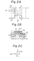
- a nonvolatile semiconductor memory circuit provided with a plurality of bit lines, a plurality of word lines, a group of nonvolatile semiconductor memory cells located at intersections of the word lines and the bit lines and formed by a MOS transistor having a floating gate and a control gate therein, a bias circuit which supplies a predetermined voltage to the control gate, and MOS transistors, formed by a depletion-type MOS transistor, located between the control gate and the bias circuit.
- FIG. 1 is an embodiment of a nonvolatile semi- conductor circuit which contains a bias circuit of the present invention.
- Memory cells which are formed by a MOS transistor 14 and a transistor 22 for selecting the transistor 14 are arranged at intersections of the row wires 13k, 13 l and the bit lines B 11 , etc B 2a .
- the selection transistor 22 is connected to the row wires 13k, 13 l and the bit lines B 11 and B 12
- the MOS transistor 14 is connected in series to the selection transistor 22, and the source of the MOS transistor 14 is connected to a source potential determination circuit 21.
- Fig. 1 eight memory cells form one unit (1 byte), and the control gate of each unit is connected via column gate transistors 15i, 15j, control gate selection column lines CGS, and row control gate selection transistors 16k, 16k 2 to the bias circuit 11.
- CLG 11 , .... CLG 18 , CLG 21 ?? CLG 28 are column selection transistors which connect the bit lines B 11 .... B28 to an output bus 17.
- the output bus is provided with a sense amplifier 18 having an input 18 in and an output 18 out Eight sense amplifiers 18 corresponding to each bit are provided (in Fig. 1, only one sense amplifier 18 for each bit is shown).
- the output data is read out of the sense ampr 18 via a buffer circuit 19.
- Fig. 1 only one example of the sense amplifier 18 is shown. Of course, the sense amplifier is not limited shown in Fig. 1, many other circuits can be used as the sense amplifier.
- the sense amplifier 18 shown in Fig. 1 is composed of depletion-type transistors 18a, 18b, and 18c and enhancement-type transistors 18c, 18d and 18f.
- the input 18. m is connected via the column selection transistors to the memory cell.
- the input 18 in assumes a low potential, the transistor 18c is turned off, the transistor 18f is turned on, and a low level voltage is generated at the output 18 out.
- a high level is output at the output 18 out .
- the selection transistor 22 When information is written into the memory cell, the selection transistor 22 is placed in the on state and a write signal is supplied to a transistor Qw , which is then placed in the on state.
- a ground potential GND is supplied via transistors 15 and 16 to the control gate CG of the selected eight-bit cell group.
- an erase signal is supplied to a transistor Q E and a voltage V pp , for example, 20 volts, is supplied to the control gate CG of the selected cell group.
- a read signal R is supplied to a transistor Q R , which is then placed in the on state (the transistors Q E and Q W are in the off state).
- the control gate bias voltage V R in the read-out state is set at V Init .
- this threshold level V Init varies, as was previously.mentioned, and can not always be maintained at a suitable value. That is, this value V Init shifts upward or downward, and this shifting is not preferable for carrying out a stable and exact read-out operation.
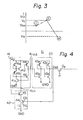
- FIG. 4 shows a diagram of the bias circuit 11 according to the present invention.
- the bias circuit 11 comprises a dummy sense amplifier 41 (which has substantially the same construction as the sense amplifier 18), a dummy cell 42, and a voltage setting circuit 43.
- control gate voltage can be advantageously varied by adjusting preliminarily the output 41 out and by obtaining an optimum output V out so that the relationship between the current i and the output 41 out varies.
- the elements in the circuit 43 are determined so as to obtain a predetermined output V out .
- the voltage V pp is supplied to.the control gate of the MOS transistor without the voltage value being decreased. Further, when the MOS transistor 14 is placed in the non-selected state, the voltage at the control gate of the MOS transistor 14 is switched to a value about 2 V higher than the voltage potential "0" V at the control gate of each of the transistors 25i, 25j, 26k 1 26k 2 , 26l 1 and 26l 2 , with the difference in voltage being
Landscapes
- Engineering & Computer Science (AREA)
- Microelectronics & Electronic Packaging (AREA)
- Read Only Memory (AREA)
Applications Claiming Priority (4)
| Application Number | Priority Date | Filing Date | Title |
|---|---|---|---|
| JP211398/81 | 1981-12-29 | ||
| JP56211398A JPS6038798B2 (ja) | 1981-12-29 | 1981-12-29 | 不揮発性半導体メモリ回路 |
| JP213401/81 | 1981-12-29 | ||
| JP56213401A JPS6038799B2 (ja) | 1981-12-29 | 1981-12-29 | 不揮発性半導体メモリ回路 |
Publications (3)
| Publication Number | Publication Date |
|---|---|
| EP0085260A2 true EP0085260A2 (fr) | 1983-08-10 |
| EP0085260A3 EP0085260A3 (en) | 1983-11-16 |
| EP0085260B1 EP0085260B1 (fr) | 1989-08-02 |
Family
ID=26518616
Family Applications (1)
| Application Number | Title | Priority Date | Filing Date |
|---|---|---|---|
| EP82306993A Expired EP0085260B1 (fr) | 1981-12-29 | 1982-12-30 | Circuit de mémoire non-volatile à semi-conducteurs |
Country Status (4)
| Country | Link |
|---|---|
| US (1) | US4677590A (fr) |
| EP (1) | EP0085260B1 (fr) |
| DE (1) | DE3279855D1 (fr) |
| IE (1) | IE55327B1 (fr) |
Cited By (2)
| Publication number | Priority date | Publication date | Assignee | Title |
|---|---|---|---|---|
| WO1997038423A1 (fr) * | 1996-04-05 | 1997-10-16 | Advanced Micro Devices, Inc. | Memoire tampon assurant la verification ou la lecture en parallele de cellules sur une ligne de mot a l'aide d'un signal provenant d'une cellule de reference dans une memoire flash |
| EP0872850A1 (fr) * | 1997-04-14 | 1998-10-21 | STMicroelectronics S.r.l. | Circuit de lecture analogique de haute précision pour réseaux de mémoire, en particulier pour réseaux de mémoire analogique flash |
Families Citing this family (46)
| Publication number | Priority date | Publication date | Assignee | Title |
|---|---|---|---|---|
| IT1213228B (it) * | 1984-10-23 | 1989-12-14 | Ates Componenti Elettron | Metodo di scrittura per matrice di celle di memoria non volatile di tipo merged. |
| JP2504743B2 (ja) * | 1985-03-18 | 1996-06-05 | 日本電気株式会社 | 半導体記憶装置 |
| JPS6240697A (ja) * | 1985-08-16 | 1987-02-21 | Fujitsu Ltd | 半導体記憶装置 |
| EP0254750B1 (fr) * | 1986-06-27 | 1993-12-29 | Nec Corporation | Système de mémoire semi-conductrice |
| JPS63121197A (ja) * | 1986-11-07 | 1988-05-25 | Fujitsu Ltd | 半導体記憶装置 |
| JPS63239694A (ja) * | 1987-03-27 | 1988-10-05 | Toshiba Corp | 半導体記憶装置 |
| US4797856A (en) * | 1987-04-16 | 1989-01-10 | Intel Corporation | Self-limiting erase scheme for EEPROM |
| IT1214246B (it) * | 1987-05-27 | 1990-01-10 | Sgs Microelettronica Spa | Dispositivo di memoria non volatile ad elevato numero di cicli di modifica. |
| JP2685770B2 (ja) * | 1987-12-28 | 1997-12-03 | 株式会社東芝 | 不揮発性半導体記憶装置 |
| USRE35838E (en) * | 1987-12-28 | 1998-07-07 | Kabushiki Kaisha Toshiba | Electrically erasable programmable read-only memory with NAND cell structure |
| US4855955A (en) * | 1988-04-08 | 1989-08-08 | Seeq Technology, Inc. | Three transistor high endurance eeprom cell |
| US5022009A (en) * | 1988-06-02 | 1991-06-04 | Mitsubishi Denki Kabushiki Kaisha | Semiconductor memory device having reading operation of information by differential amplification |
| JPH0770235B2 (ja) * | 1988-06-24 | 1995-07-31 | 株式会社東芝 | 不揮発性メモリ回路装置 |
| US4851720A (en) * | 1988-09-02 | 1989-07-25 | Cypress Semiconductor Corporation | Low power sense amplifier for programmable logic device |
| JP2718716B2 (ja) * | 1988-09-30 | 1998-02-25 | 株式会社東芝 | 不揮発性半導体メモリ装置およびそのデータ書替え方法 |
| JP2573335B2 (ja) * | 1988-11-09 | 1997-01-22 | 株式会社東芝 | 不揮発性メモリ |
| US5138575A (en) * | 1988-12-19 | 1992-08-11 | Fujitsu Limited | Electricaly erasable and programmable read only memory with a discharge device |
| US5088060A (en) * | 1989-03-08 | 1992-02-11 | Kabushiki Kaisha Toshiba | Electrically erasable programmable read-only memory with NAND memory cell structure |
| US4996669A (en) * | 1989-03-08 | 1991-02-26 | Kabushiki Kaisha Toshiba | Electrically erasable programmable read-only memory with NAND memory cell structure |
| GB8907045D0 (en) * | 1989-03-29 | 1989-05-10 | Hughes Microelectronics Ltd | Sense amplifier |
| DE69024086T2 (de) * | 1989-04-13 | 1996-06-20 | Sundisk Corp | EEprom-System mit Blocklöschung |
| US7447069B1 (en) | 1989-04-13 | 2008-11-04 | Sandisk Corporation | Flash EEprom system |
| US5247480A (en) * | 1989-05-02 | 1993-09-21 | Kabushiki Kaisha Toshiba | Electrically erasable progammable read-only memory with nand cell blocks |
| US5283758A (en) * | 1989-06-13 | 1994-02-01 | Mitsubishi Denki Kabushiki Kaisha | Non-volatile semiconductor memory device |
| JP2862584B2 (ja) * | 1989-08-31 | 1999-03-03 | 株式会社東芝 | 不揮発性半導体メモリ装置 |
| US5065364A (en) * | 1989-09-15 | 1991-11-12 | Intel Corporation | Apparatus for providing block erasing in a flash EPROM |
| KR930000869B1 (ko) * | 1989-11-30 | 1993-02-08 | 삼성전자 주식회사 | 페이지 소거 가능한 플래쉬형 이이피롬 장치 |
| JP2606941B2 (ja) * | 1990-02-19 | 1997-05-07 | 富士通株式会社 | 不揮発性メモリの書込み回路 |
| JP3448051B2 (ja) * | 1990-03-31 | 2003-09-16 | 株式会社東芝 | 不揮発性半導体記憶装置 |
| US5287536A (en) * | 1990-04-23 | 1994-02-15 | Texas Instruments Incorporated | Nonvolatile memory array wordline driver circuit with voltage translator circuit |
| JP3060680B2 (ja) * | 1990-11-30 | 2000-07-10 | 日本電気株式会社 | 不揮発性半導体記憶装置 |
| KR940005695B1 (ko) * | 1990-12-19 | 1994-06-22 | 삼성전자 주식회사 | 불휘발성 기억소자의 로우 디코더 회로 |
| DE4205061C2 (de) * | 1991-02-19 | 2000-04-06 | Toshiba Kawasaki Kk | Nichtflüchtige Halbleiter-Speicheranordnung |
| US5265059A (en) * | 1991-05-10 | 1993-11-23 | Intel Corporation | Circuitry and method for discharging a drain of a cell of a non-volatile semiconductor memory |
| US5295104A (en) * | 1991-12-17 | 1994-03-15 | Sgs-Thomson Microelectronics, Inc. | Integrated circuit with precharged internal data bus |
| DE4302195C2 (de) * | 1993-01-27 | 1996-12-19 | Telefunken Microelectron | Verfahren zum Betrieb eines nichtflüchtigen Halbleiterspeichers |
| US5532623A (en) * | 1994-10-21 | 1996-07-02 | Waferscale Integration, Inc. | Sense amplifier with read current tracking and zero standby power consumption |
| KR0164354B1 (ko) * | 1994-12-12 | 1999-02-18 | 김광호 | 불휘발성 메모리 장치의 데이타 독출 교란방지 회로 |
| JP3636497B2 (ja) * | 1995-02-27 | 2005-04-06 | 株式会社ルネサステクノロジ | 半導体集積回路装置 |
| US5815435A (en) * | 1995-10-10 | 1998-09-29 | Information Storage Devices, Inc. | Storage cell for analog recording and playback |
| US6137720A (en) * | 1997-11-26 | 2000-10-24 | Cypress Semiconductor Corporation | Semiconductor reference voltage generator having a non-volatile memory structure |
| US6128229A (en) * | 1998-09-16 | 2000-10-03 | Sony Corporation | Non-volatile semiconductor memory and method of verifying after writing and reading the same |
| JP3717388B2 (ja) * | 2000-09-27 | 2005-11-16 | 株式会社リコー | 基準電圧発生回路及びその出力値調整方法並びに電源装置 |
| US8320191B2 (en) | 2007-08-30 | 2012-11-27 | Infineon Technologies Ag | Memory cell arrangement, method for controlling a memory cell, memory array and electronic device |
| US9281032B2 (en) | 2014-04-10 | 2016-03-08 | Infineon Technologies Ag | Memory timing circuit |
| CN115485838A (zh) * | 2020-04-30 | 2022-12-16 | 华为技术有限公司 | 一种集成电路 |
Family Cites Families (10)
| Publication number | Priority date | Publication date | Assignee | Title |
|---|---|---|---|---|
| DE2514582C2 (de) * | 1975-04-03 | 1977-05-26 | Siemens Ag | Schaltung zur erzeugung von leseimpulsen |
| US4099264A (en) * | 1976-10-28 | 1978-07-04 | Sperry Rand Corporation | Non-destructive interrogation control circuit for a variable threshold FET memory |
| JPS54137933A (en) * | 1978-04-18 | 1979-10-26 | Sharp Corp | Programmable nonvolatile rom |
| US4223394A (en) * | 1979-02-13 | 1980-09-16 | Intel Corporation | Sensing amplifier for floating gate memory devices |
| US4266283A (en) * | 1979-02-16 | 1981-05-05 | Intel Corporation | Electrically alterable read-mostly memory |
| GB2049327B (en) * | 1979-05-14 | 1983-03-30 | Fairchild Camera Instr Co | Memory read voltage circuitry for adapting eproms to circuits employing substrate bias voltage |
| US4301535A (en) * | 1979-07-02 | 1981-11-17 | Mostek Corporation | Programmable read only memory integrated circuit with bit-check and deprogramming modes and methods for programming and testing said circuit |
| JPS5654693A (en) * | 1979-10-05 | 1981-05-14 | Hitachi Ltd | Programable rom |
| JPS5819795A (ja) * | 1981-07-29 | 1983-02-04 | Toshiba Corp | メモリ出力読取回路 |
| EP0088815B1 (fr) * | 1982-03-17 | 1985-12-18 | Deutsche ITT Industries GmbH | Matrice de mémoire effaçable électriquement (EEPROM) |
-
1982
- 1982-12-30 EP EP82306993A patent/EP0085260B1/fr not_active Expired
- 1982-12-30 DE DE8282306993T patent/DE3279855D1/de not_active Expired
- 1982-12-30 IE IE3103/82A patent/IE55327B1/en not_active IP Right Cessation
-
1986
- 1986-03-24 US US06/844,257 patent/US4677590A/en not_active Expired - Fee Related
Cited By (3)
| Publication number | Priority date | Publication date | Assignee | Title |
|---|---|---|---|---|
| WO1997038423A1 (fr) * | 1996-04-05 | 1997-10-16 | Advanced Micro Devices, Inc. | Memoire tampon assurant la verification ou la lecture en parallele de cellules sur une ligne de mot a l'aide d'un signal provenant d'une cellule de reference dans une memoire flash |
| EP0872850A1 (fr) * | 1997-04-14 | 1998-10-21 | STMicroelectronics S.r.l. | Circuit de lecture analogique de haute précision pour réseaux de mémoire, en particulier pour réseaux de mémoire analogique flash |
| US6016272A (en) * | 1997-04-14 | 2000-01-18 | Stmicroelectronicss. R. L. | High-precision analog reading circuit for flash analog memory arrays using negative feedback |
Also Published As
| Publication number | Publication date |
|---|---|
| IE55327B1 (en) | 1990-08-15 |
| US4677590A (en) | 1987-06-30 |
| IE823103L (en) | 1983-06-29 |
| DE3279855D1 (en) | 1989-09-07 |
| EP0085260A3 (en) | 1983-11-16 |
| EP0085260B1 (fr) | 1989-08-02 |
Similar Documents
| Publication | Publication Date | Title |
|---|---|---|
| EP0085260B1 (fr) | Circuit de mémoire non-volatile à semi-conducteurs | |
| US4266283A (en) | Electrically alterable read-mostly memory | |
| US5276646A (en) | High voltage generating circuit for a semiconductor memory circuit | |
| KR100190089B1 (ko) | 플래쉬 메모리장치 및 그 구동방법 | |
| US5357465A (en) | Single transistor EEPROM memory cell | |
| US6011747A (en) | Memory cell of non-volatile semiconductor memory device | |
| EP0899744A2 (fr) | Procédé et appareil pour programmation d'un dispositif de mémoire tel qu'une cellule de réseau de flash EPROM de type masse virtuelle | |
| US4737936A (en) | Semiconductor memory device having improved write-verify operation | |
| US6744673B2 (en) | Feedback biasing integrated circuit | |
| US6163481A (en) | Flash memory wordline tracking across whole chip | |
| EP0842514B1 (fr) | Systeme de memoire flash a perturbations reduites et procede | |
| KR20010100877A (ko) | 플래시 이이피롬 워드라인 드라이버 | |
| EP0443777B1 (fr) | Circuit d'écriture pour dispositif de mémoire non volatile | |
| US6643210B2 (en) | Semiconductor integrated circuit device and method of controlling the same | |
| JP3342878B2 (ja) | 不揮発性半導体記憶装置 | |
| US6137727A (en) | Reduction of oxide stress through the use of forward biased body voltage | |
| JPS6038799B2 (ja) | 不揮発性半導体メモリ回路 | |
| US6195295B1 (en) | Segmented column memory device voltage steering technique | |
| JP3094905B2 (ja) | 不揮発性半導体記憶装置 | |
| JPH0528778A (ja) | 不揮発性半導体記憶装置 | |
| KR100200918B1 (ko) | 소거 검증을 위한 불휘발성 반도체 메모리 장치 | |
| JP3190082B2 (ja) | 半導体記憶装置 | |
| JPH0528782A (ja) | 不揮発性半導体記憶装置 | |
| JP3476866B2 (ja) | 半導体記憶装置 | |
| JPH01235097A (ja) | 不揮発性半導体メモリ |
Legal Events
| Date | Code | Title | Description |
|---|---|---|---|
| PUAI | Public reference made under article 153(3) epc to a published international application that has entered the european phase |
Free format text: ORIGINAL CODE: 0009012 |
|
| AK | Designated contracting states |
Designated state(s): DE FR GB |
|
| PUAL | Search report despatched |
Free format text: ORIGINAL CODE: 0009013 |
|
| AK | Designated contracting states |
Designated state(s): DE FR GB |
|
| 17P | Request for examination filed |
Effective date: 19840515 |
|
| GRAA | (expected) grant |
Free format text: ORIGINAL CODE: 0009210 |
|
| AK | Designated contracting states |
Kind code of ref document: B1 Designated state(s): DE FR GB |
|
| REF | Corresponds to: |
Ref document number: 3279855 Country of ref document: DE Date of ref document: 19890907 |
|
| ET | Fr: translation filed | ||
| PLBE | No opposition filed within time limit |
Free format text: ORIGINAL CODE: 0009261 |
|
| STAA | Information on the status of an ep patent application or granted ep patent |
Free format text: STATUS: NO OPPOSITION FILED WITHIN TIME LIMIT |
|
| 26N | No opposition filed | ||
| PGFP | Annual fee paid to national office [announced via postgrant information from national office to epo] |
Ref country code: FR Payment date: 19941209 Year of fee payment: 13 |
|
| PGFP | Annual fee paid to national office [announced via postgrant information from national office to epo] |
Ref country code: GB Payment date: 19941220 Year of fee payment: 13 |
|
| PGFP | Annual fee paid to national office [announced via postgrant information from national office to epo] |
Ref country code: DE Payment date: 19941222 Year of fee payment: 13 |
|
| PG25 | Lapsed in a contracting state [announced via postgrant information from national office to epo] |
Ref country code: GB Effective date: 19951230 |
|
| GBPC | Gb: european patent ceased through non-payment of renewal fee |
Effective date: 19951230 |
|
| PG25 | Lapsed in a contracting state [announced via postgrant information from national office to epo] |
Ref country code: FR Effective date: 19960830 |
|
| PG25 | Lapsed in a contracting state [announced via postgrant information from national office to epo] |
Ref country code: DE Effective date: 19960903 |
|
| REG | Reference to a national code |
Ref country code: FR Ref legal event code: ST |
|
| APAH | Appeal reference modified |
Free format text: ORIGINAL CODE: EPIDOSCREFNO |