EP0085607A2 - Verfahren zur gleichzeitigen Produktion von Hyperfrequenzdioden mit eingebauter Einkapselung und nach diesem Verfahren hergestellte Dioden - Google Patents
Verfahren zur gleichzeitigen Produktion von Hyperfrequenzdioden mit eingebauter Einkapselung und nach diesem Verfahren hergestellte Dioden Download PDFInfo
- Publication number
- EP0085607A2 EP0085607A2 EP83400164A EP83400164A EP0085607A2 EP 0085607 A2 EP0085607 A2 EP 0085607A2 EP 83400164 A EP83400164 A EP 83400164A EP 83400164 A EP83400164 A EP 83400164A EP 0085607 A2 EP0085607 A2 EP 0085607A2
- Authority
- EP
- European Patent Office
- Prior art keywords
- face
- dielectric material
- semiconductor
- layer
- collective
- Prior art date
- Legal status (The legal status is an assumption and is not a legal conclusion. Google has not performed a legal analysis and makes no representation as to the accuracy of the status listed.)
- Withdrawn
Links
Images


Classifications
-
- H—ELECTRICITY
- H10—SEMICONDUCTOR DEVICES; ELECTRIC SOLID-STATE DEVICES NOT OTHERWISE PROVIDED FOR
- H10P—GENERIC PROCESSES OR APPARATUS FOR THE MANUFACTURE OR TREATMENT OF DEVICES COVERED BY CLASS H10
- H10P54/00—Cutting or separating of wafers, substrates or parts of devices
-
- H—ELECTRICITY
- H10—SEMICONDUCTOR DEVICES; ELECTRIC SOLID-STATE DEVICES NOT OTHERWISE PROVIDED FOR
- H10W—GENERIC PACKAGES, INTERCONNECTIONS, CONNECTORS OR OTHER CONSTRUCTIONAL DETAILS OF DEVICES COVERED BY CLASS H10
- H10W20/00—Interconnections in chips, wafers or substrates
- H10W20/40—Interconnections external to wafers or substrates, e.g. back-end-of-line [BEOL] metallisations or vias connecting to gate electrodes
Definitions
- the present invention relates to a process for the collective production of devices having two metallized faces, for example diodes.
- These devices are in the form of elements having an incorporated encapsulation and do not require housings. They are particularly well suited to the case of Gunn or avalanche diodes.
- the fact of being able to easily control the geometric dimensions of these diodes makes it possible to use them advantageously in millimeter wave sources in the solid state by carrying out a radial impedance transformation.
- the invention also relates to a semiconductor device comprising a support having a first and a second metallized face, a semiconductor wafer included in said support and adjacent to said first face, an annular cup formed around said wafer from said first. face, the depth of said annular cup being at least equal to the thickness of said pellet and being filled with a dielectric material, characterized in that said device further comprises a central cup formed from said second face, the bottom of said central bowl joining said patch and the rim of said central bowl being formed by a part of said second face.
- a series of layers of different conductivity types are grown by epitaxy on a monocrystalline silicon washer of high resistivity, which will form a semiconductor structure.
- S the section of the washer, W its thickness, p its resistivity and e its dielectric constant.
- the washer will behave all the more like a dielectric as the current passing through the washer subjected to an electric pulsating voltage ⁇ between its two faces will be much more obtained by the capacitive effect than by the resistive effect of the electrical diagram equivalent to the washer. This is achieved if: ⁇ ⁇ ⁇ »1.
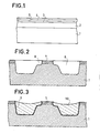
- FIG. 1 is a sectional view of part of the washer. We see the original washer 1. which is little or not doped against the usual manufacturing processes for which we generally started from an N + doped substrate . The thickness of this washer is approximately 100 microns for technical reasons which will be explained below. Its resistivity is around 4000 ⁇ .cm or more. The first layer developed on the washer is layer 2 N + doped with a resistivity of 0.003 n .cm and around 5 to 10 microns thick.
- the groove was produced according to a particular profile as represented by the section in FIG. 2.
- This profile was obtained by chemical attack carried out in two stages. For example, with a first mask, the washer was attacked until it reached the depth corresponding to the shoulder 8, then with a second mask with a smaller surface, the attack on the washer was resumed so as to get the profile shown.
- FIG. 2 the section of which has been made along a diameter of the groove 6, the shoulder 8 is noted, the depth of which is approximately equal to the total thickness of the epitaxial layers.
- the groove walls are preferably covered with a thin barrier film 9 which is made of a material resistant to the chemical agent which will be used later during an attack phase.
- a thin barrier film 9 which is made of a material resistant to the chemical agent which will be used later during an attack phase.
- silicon nitride Si 3 N4 or silica Si0 2 can be used, which resists a chemical agent for attacking silicon, such as a mixture of nitric acid and hydrofluoric acid, then these grooves are filled. by a dielectric material. It is advantageous to carry out this filling with molten glass which has fairly good dielectric properties at the frequencies considered as well as good mechanical properties. In addition, this dielectric must be able to withstand the high temperatures which are encountered in avalanche diodes (up to 300 ° C).
- the outside diameter of the groove is of the order of magnitude of the half-wavelength, in the dielectric considered, of the electrical signals used in this type of device.
- the quantity of glass is dosed so that its surface is flat or slightly concave.
- FIG. 3 represents a fraction of the washer 1 in section.
- the stop layer 9 covering the walls of the groove, which has been filled with molten glass 10.
- the quantity of glass has been dosed so as to have a slight concavity on the surface. This allows the diode to be welded upside down without the need for a large thickness of metallization and soldering. This reverse soldering is a necessity for avalanche diodes.
- dielectrics other than glass for example polymerizable materials.
- the thickness of the washer has been deliberately chosen to be greater than 100 microns in order to be able to correctly produce grooves whose maximum depth is approximately 30 microns and to fill them with dielectric.
- the choice of an original washer of smaller thickness could pose problems due to mechanical stresses.
- the step represented in FIG. 4 consists in running in the washer on the intrinsic side if necessary in order to bring it to the desired thickness, and to minimize the losses that too thick a silicon could introduce despite its high resistivity. We can even consider continuing to run in until the glass begins. In the case represented by FIG. 4, we have chosen to have E 2 much smaller than E l "
- the areas of the washer internal to the annular grooves are chemically attacked using a masking technique.
- This attack is carried out until the first epitaxial layer adjacent to the substrate 1 at the same removing a portion of this N + region.
- the thickness of the junction can be checked by an infrared transparency test.
- This attack is preferably carried out in reactive plasma because of the possible anisotropy of the attack.
- FIG. 5 shows the result obtained at the end of this attack.
- the masking used made it possible to keep a certain part of the substrate under the furrow and to form a central bowl.
- This central cuvette therefore has a layer of the semiconductor wafer for its background and a portion of the face of the substrate from which the attack was conducted for its rim.
- the barrier layer 9 avoided the possible attack of the glass by the chemical agent. This gives a junction limited to its active part and inserted into a support with controlled dimensions.
- the step represented by FIG. 6 consists in metallizing the access faces of the junction in order to make connections.
- J1 is advantageous to extend the metallizations on each face of the washer by operating, for example, by sputtering.
- An advantageous method consists in first depositing on each face of the junction a layer (11, 12) of platinum and of forming platinum silicide by heat treatment at a temperature of about 400 ° C., then successive deposits on all or part of the faces of the titanium, platinum and gold washer.
- All of the titanium-platinum-gold deposits are represented in FIG. 6 by the layers 13 and 14.
- the part of the junction which heats up. plus is the upper part, if we consider figure 6, that is to say that which is close to the metallization layers 11 and 13.
- the embodiment of the diode according to the invention has the advantage of freeing as much as possible the side of the junction which heats the most from its support, especially if the dielectric 10 has its slightly concave free surface.
- the avalanche diodes are generally welded by reverse welding, that is to say on the metallization 13 (Ti-Pt Au).
- an electrolytic growth of gold is provided for the contact 13 which serves as a thermal and mechanical damper between the solder and the diode.
- the thickness of the layer may be limited. gold for example at 2 microns and operate by thermocompression so that the heat is dissipated as much as possible by the diamond. If the diode is to be used in pulsed mode the heat generated during the use of the diode is distributed almost equally on each side of the junction and in this case it is advantageous to provide a thicker layer of gold for the contact 14.
- the step represented by FIG. 7 consists in the separation of the diodes by cutting, for example by chemical attack.
- Figure 7 shows a diode thus obtained. It is characterized by its geometric dimensions, for example its outside diameter, which are important in many applications.
- the cutting can also contribute to removing part of the dielectric material 10.
- the zone 15 formed of epitaxial layers is preferably kept when a reverse weld is desired. Indeed, this zone is located in the same plane as the junction and contributes during the welding to have a good flatness of the device.
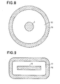
- each diode is in the form of a small disc as shown in FIG. 8 which is a top view of a diode from which the metallizations 11 and 13 have been removed.
- junction 7 at the center of the dielectric 10 which is itself surrounded by a ring 15 formed from the residues of the epitaxial layers.
- junction 16 It is also part of the invention to give the junction a square or rectangular shape whose surfaces in contact with the metallizations are in the form of elongated rectangles which tend to reduce the thermal resistance between the junction and the metal contacts liques.
- Figure 9 is a top view of such an embodiment where the metallizations have been removed in order to access the junction. It has been found preferable in this case to give the assembly an equally rectangular shape, but this is not an obligation.
- the cutting can be done with a saw or possibly by chemical attack, preferably very anisotropic.
- junction 16 surrounded by a dielectric 17, which may be glass as before and a frame 18 of the same nature as junction 16.
- the hollow shape of the metallization 14 nevertheless makes it easy to make contact with a connection on this face of the diode by simply pressing a rod in the use cavity.
- FIG. 11 shows the same diode at avalanche than that described above for which the original substrate 1 has been completely eliminated, the latter can then have any resistivity.
- FIG. 12 Another possible cut is that which gave rise to the device represented in FIG. 12 which retains a part 26 of the substrate 1. It will be noted that there is no longer any semiconductor material connecting the electrodes. In this case, if the grooves are sufficiently deep, the material forming the substrate does not need to have a very high resistivity. On the contrary, it must have a very low resistivity so as not to introduce losses.
- a variant of the manufacturing process consists in depositing between the substrate and the epitaxial layers a barrier layer.
- a barrier layer In this case, to produce, for example, an avalanche diode with a double sliding zone similar to that described above, it is possible to start from an N + doped semiconductor substrate in the form of a washer with a diameter of about two inches and 100 microns thick.
- FIG. 13 which is a partial view, there is the substrate 22 on which a stop layer 20 has been deposited.
- This stop layer can be made of silicon oxide Si0 2 , of silicon nitride Si 3 N 4 or by a mixture of these two products.
- This high resistivity can be obtained for example by lightly doping the silicon with oxygen or nitrogen.
- the growth conditions of this layer are adjusted to ensure excellent flatness of the upper face of the layer 22.
- This layer 22. is then thinned by lapping and / or chemical attack to a thickness of approximately 5 to 10 microns.
- an N-doped layer 23, a P-doped layer 24 and a P + doped layer 25 are developed by epitaxy on the layer 22.
- the impurity concentrations and the thicknesses of the layers 22 to 25 are of the same order of magnitude as the corresponding layers of the avalanche diode described above.
- the manufacturing process then repeats the steps described above.
- the advantage of this variant is that the chemical attack on the rear face, that is to say the attack on the substrate in the direction of the layer 22, stops on the barrier layer 20. This layer d The stop 20 must be partially eliminated to ensure contact with the layer 22. This is done by selective chemical attack or rather by ionic machining which ensures better control of the attack.
- the groove may have a depth greater than or equal to the thickness of the semiconductor structure forming the diode. If the groove has a thickness greater than the thickness of the structure, the chemical attack contributing to digging this groove must be capable of partially eliminating the stop layer 20 and coming to bite into the substrate 21.
- the invention also applies to any diode that one wishes to mount on the spot. It also applies to diodes made from arsenide of gallium, in particular to Gunn diodes, to mixing diodes and possibly to varicap diodes. In this case, it is appropriate to use the method according to the invention in connection with the technology suitable for gallium arsenide.
Landscapes
- Electrodes Of Semiconductors (AREA)
- Semiconductor Integrated Circuits (AREA)
- Bipolar Transistors (AREA)
Applications Claiming Priority (2)
| Application Number | Priority Date | Filing Date | Title |
|---|---|---|---|
| FR8201651A FR2520931B1 (fr) | 1982-02-02 | 1982-02-02 | Procede collectif de fabrication de diodes hyperfrequences avec encapsulation incorporee et diodes obtenues par ce procede |
| FR8201651 | 1982-02-02 |
Publications (2)
| Publication Number | Publication Date |
|---|---|
| EP0085607A2 true EP0085607A2 (de) | 1983-08-10 |
| EP0085607A3 EP0085607A3 (de) | 1983-08-24 |
Family
ID=9270586
Family Applications (1)
| Application Number | Title | Priority Date | Filing Date |
|---|---|---|---|
| EP83400164A Withdrawn EP0085607A3 (de) | 1982-02-02 | 1983-01-25 | Verfahren zur gleichzeitigen Produktion von Hyperfrequenzdioden mit eingebauter Einkapselung und nach diesem Verfahren hergestellte Dioden |
Country Status (4)
| Country | Link |
|---|---|
| EP (1) | EP0085607A3 (de) |
| JP (1) | JPS58134486A (de) |
| CA (1) | CA1203638A (de) |
| FR (1) | FR2520931B1 (de) |
Cited By (8)
| Publication number | Priority date | Publication date | Assignee | Title |
|---|---|---|---|---|
| FR2559959A1 (fr) * | 1984-02-21 | 1985-08-23 | Thomson Csf | Diode hyperfrequence a connexions externes prises au moyen de poutres et son procede de realisation |
| FR2565030A1 (fr) * | 1984-05-25 | 1985-11-29 | Thomson Csf | Structure de metallisations de reprise de contacts d'un dispositif semi-conducteur et dispositif dote d'une telle structure |
| EP0303390A1 (de) * | 1987-08-14 | 1989-02-15 | Marconi Electronic Devices Limited | Herstellung von Dioden |
| DE4209983A1 (de) * | 1992-03-27 | 1993-09-30 | Daimler Benz Ag | Verfahren zur Herstellung von in einem Gehäuse angeordneten Halbleiterbauelementen |
| EP0603971A3 (de) * | 1992-12-23 | 1995-06-28 | Koninkl Philips Electronics Nv | Halbleiteranordnung mit passivierten Seitenflächen und Verfahren zu ihrer Herstellung. |
| EP0627764A3 (de) * | 1993-05-27 | 1995-12-06 | Siemens Ag | Verfahren zur Vereinzelung von Chips auf einem Wafer. |
| WO2000035001A1 (de) * | 1998-12-07 | 2000-06-15 | Robert Bosch Gmbh | Verfahren zur eingehäusung elektronischer bauelemente |
| US10478289B2 (en) | 2003-12-23 | 2019-11-19 | Boston Scientific Scimed, Inc. | Replacement valve and anchor |
Families Citing this family (1)
| Publication number | Priority date | Publication date | Assignee | Title |
|---|---|---|---|---|
| DE102007007159B4 (de) * | 2007-02-09 | 2009-09-03 | Technische Universität Darmstadt | Gunn-Diode |
Family Cites Families (3)
| Publication number | Priority date | Publication date | Assignee | Title |
|---|---|---|---|---|
| US4180422A (en) * | 1969-02-03 | 1979-12-25 | Raytheon Company | Method of making semiconductor diodes |
| GB2028583B (en) * | 1978-08-02 | 1983-01-06 | Aei Semiconductors Ltd | Electrical lead for a semiconductor device |
| GB2067354B (en) * | 1980-01-09 | 1984-04-18 | Aei Semiconductors Ltd | Mounting for a sc device |
-
1982
- 1982-02-02 FR FR8201651A patent/FR2520931B1/fr not_active Expired
-
1983
- 1983-01-25 EP EP83400164A patent/EP0085607A3/de not_active Withdrawn
- 1983-01-28 CA CA000420415A patent/CA1203638A/en not_active Expired
- 1983-02-01 JP JP58015385A patent/JPS58134486A/ja active Pending
Cited By (9)
| Publication number | Priority date | Publication date | Assignee | Title |
|---|---|---|---|---|
| FR2559959A1 (fr) * | 1984-02-21 | 1985-08-23 | Thomson Csf | Diode hyperfrequence a connexions externes prises au moyen de poutres et son procede de realisation |
| FR2565030A1 (fr) * | 1984-05-25 | 1985-11-29 | Thomson Csf | Structure de metallisations de reprise de contacts d'un dispositif semi-conducteur et dispositif dote d'une telle structure |
| EP0166633A1 (de) * | 1984-05-25 | 1986-01-02 | Thomson-Csf | Metallisierungsstruktur zur Kontaktherstellung für eine Halbleitervorrichtung und Vorrichtung mit einer solchen Struktur |
| EP0303390A1 (de) * | 1987-08-14 | 1989-02-15 | Marconi Electronic Devices Limited | Herstellung von Dioden |
| DE4209983A1 (de) * | 1992-03-27 | 1993-09-30 | Daimler Benz Ag | Verfahren zur Herstellung von in einem Gehäuse angeordneten Halbleiterbauelementen |
| EP0603971A3 (de) * | 1992-12-23 | 1995-06-28 | Koninkl Philips Electronics Nv | Halbleiteranordnung mit passivierten Seitenflächen und Verfahren zu ihrer Herstellung. |
| EP0627764A3 (de) * | 1993-05-27 | 1995-12-06 | Siemens Ag | Verfahren zur Vereinzelung von Chips auf einem Wafer. |
| WO2000035001A1 (de) * | 1998-12-07 | 2000-06-15 | Robert Bosch Gmbh | Verfahren zur eingehäusung elektronischer bauelemente |
| US10478289B2 (en) | 2003-12-23 | 2019-11-19 | Boston Scientific Scimed, Inc. | Replacement valve and anchor |
Also Published As
| Publication number | Publication date |
|---|---|
| FR2520931A1 (fr) | 1983-08-05 |
| FR2520931B1 (fr) | 1986-12-12 |
| JPS58134486A (ja) | 1983-08-10 |
| EP0085607A3 (de) | 1983-08-24 |
| CA1203638A (en) | 1986-04-22 |
Similar Documents
| Publication | Publication Date | Title |
|---|---|---|
| EP3657556B1 (de) | Herstellungsverfahren mindestens einer passivierten planaren fotodiode mit reduziertem dunkelstrom | |
| EP3127142B1 (de) | Verfahren zur herstellung eines halbleiterwafers zur herstellung eines soi-substrats und damit hergestellter soi-substratwafer | |
| EP3660930B1 (de) | Herstellungsverfahren einer fotodiodenmatrix auf germaniumbasis und mit schwachem dunkelstrom | |
| EP0801419A1 (de) | Herstellungsverfahren von einem dünnen Halbleiterfilm, der elektronische Anordnungen enthält | |
| EP3394908B1 (de) | Substrat für eine temperaturkompensierte oberflächenschallwellenvorrichtung oder volumenschallwellenvorrichtung | |
| FR2517122A1 (fr) | Dispositif semi-conducteur, notamment diode micro-ondes et son procede de fabrication | |
| EP3818561B1 (de) | Substrat für eine integrierte hochfrequenzvorrichtung und verfahren zur herstellung davon | |
| EP2144369A1 (de) | Volumenwellenresonator | |
| WO2008074862A1 (fr) | Procede de realisation de microfils et/ou de nanofils | |
| EP0461967A2 (de) | Halbleiteranordnung mit Schottky-Übergang für Mikrowellenverstärkung und schnelle logische Schaltungen und Verfahren zu deren Herstellung | |
| WO2020128354A1 (fr) | Substrat de type semi-conducteur sur isolant pour des applications radiofréquences | |
| FR2813993A1 (fr) | Dispositif de semi-conducteur | |
| EP0085607A2 (de) | Verfahren zur gleichzeitigen Produktion von Hyperfrequenzdioden mit eingebauter Einkapselung und nach diesem Verfahren hergestellte Dioden | |
| FR2538616A1 (fr) | Procede de fabrication collective de diodes hyperfrequence avec encapsulation incorporee et diodes ainsi obtenues | |
| FR2693314A1 (fr) | Transistor JFET vertical à mode de fonctionnement bipolaire optimisé et procédé de fabrication correspondant. | |
| EP2254243B1 (de) | Akustischer Volumenwellenresonator und Herstellungsverfahren dafür | |
| FR2955205A1 (fr) | Dispositif microelectronique, en particulier capteur d'image a illumination par la face arriere et procede de fabrication | |
| EP0109887B1 (de) | Hyperfrequenz-Dioden-Struktur deren äussere Verbindungen zwischen zwei metallischen Balkenleitern gefasst sind | |
| EP4354524B1 (de) | Planare photodiode auf germaniumbasis mit einer kompressiven peripheren seitlichen zone | |
| FR2805081A1 (fr) | Procede de fabrication de transistor bipolaire a double heterojonction sur materiau iii-v | |
| EP4135007A1 (de) | Verfahren zur herstellung von hochfrequenzkomponenten | |
| FR2663157A1 (fr) | Procede d'autoalignement des contacts metalliques sur un dispositif semiconducteur et semiconducteur autoaligne. | |
| EP4377491B1 (de) | Verfahren zur herstellung einer optoelektronischen vorrichtung mit einem schritt zur gleichmässig und kontinuierlichen herstellung einer dünnen leitenden schicht durch gerichtete abscheidung | |
| FR3098014A1 (fr) | Composé intermétallique | |
| FR2879820A1 (fr) | Modulateur a jonction capacitive, jonction capacitive et son procede de realisation |
Legal Events
| Date | Code | Title | Description |
|---|---|---|---|
| PUAI | Public reference made under article 153(3) epc to a published international application that has entered the european phase |
Free format text: ORIGINAL CODE: 0009012 |
|
| PUAL | Search report despatched |
Free format text: ORIGINAL CODE: 0009013 |
|
| AK | Designated contracting states |
Designated state(s): DE GB NL |
|
| AK | Designated contracting states |
Designated state(s): DE GB NL |
|
| 17P | Request for examination filed |
Effective date: 19830831 |
|
| STAA | Information on the status of an ep patent application or granted ep patent |
Free format text: STATUS: THE APPLICATION IS DEEMED TO BE WITHDRAWN |
|
| 18D | Application deemed to be withdrawn |
Effective date: 19850723 |
|
| RIN1 | Information on inventor provided before grant (corrected) |
Inventor name: HENRY, RAYMOND Inventor name: HEITZMANN, MICHEL |