EP0085991A2 - Logische Schaltung - Google Patents
Logische Schaltung Download PDFInfo
- Publication number
- EP0085991A2 EP0085991A2 EP83101284A EP83101284A EP0085991A2 EP 0085991 A2 EP0085991 A2 EP 0085991A2 EP 83101284 A EP83101284 A EP 83101284A EP 83101284 A EP83101284 A EP 83101284A EP 0085991 A2 EP0085991 A2 EP 0085991A2
- Authority
- EP
- European Patent Office
- Prior art keywords
- terminal
- field effect
- effect transistor
- transistor
- circuit
- Prior art date
- Legal status (The legal status is an assumption and is not a legal conclusion. Google has not performed a legal analysis and makes no representation as to the accuracy of the status listed.)
- Ceased
Links
- 230000005669 field effect Effects 0.000 claims abstract description 25
- 239000004065 semiconductor Substances 0.000 claims description 8
- 230000004044 response Effects 0.000 claims description 5
- 239000000758 substrate Substances 0.000 claims description 5
- 238000000034 method Methods 0.000 description 6
- 230000008569 process Effects 0.000 description 6
- 238000010586 diagram Methods 0.000 description 4
- 230000008859 change Effects 0.000 description 3
- 230000003321 amplification Effects 0.000 description 2
- 230000005540 biological transmission Effects 0.000 description 2
- 230000006870 function Effects 0.000 description 2
- 238000003199 nucleic acid amplification method Methods 0.000 description 2
- 238000010276 construction Methods 0.000 description 1
- 230000009467 reduction Effects 0.000 description 1
- 230000000630 rising effect Effects 0.000 description 1
Images


Classifications
-
- H—ELECTRICITY
- H03—ELECTRONIC CIRCUITRY
- H03K—PULSE TECHNIQUE
- H03K19/00—Logic circuits, i.e. having at least two inputs acting on one output; Inverting circuits
- H03K19/02—Logic circuits, i.e. having at least two inputs acting on one output; Inverting circuits using specified components
- H03K19/08—Logic circuits, i.e. having at least two inputs acting on one output; Inverting circuits using specified components using semiconductor devices
- H03K19/094—Logic circuits, i.e. having at least two inputs acting on one output; Inverting circuits using specified components using semiconductor devices using field-effect transistors
- H03K19/0944—Logic circuits, i.e. having at least two inputs acting on one output; Inverting circuits using specified components using semiconductor devices using field-effect transistors using MOSFET or insulated gate field-effect transistors, i.e. IGFET
- H03K19/09441—Logic circuits, i.e. having at least two inputs acting on one output; Inverting circuits using specified components using semiconductor devices using field-effect transistors using MOSFET or insulated gate field-effect transistors, i.e. IGFET of the same canal type
- H03K19/09443—Logic circuits, i.e. having at least two inputs acting on one output; Inverting circuits using specified components using semiconductor devices using field-effect transistors using MOSFET or insulated gate field-effect transistors, i.e. IGFET of the same canal type using a combination of enhancement and depletion transistors
Definitions
- the present invention relates to a logic circuit employing field effect transistors, and more particularly to an E/D type logic circuit whose input-output characteristics have a hysteresis.
- the E/D type logic circuit comprises a depletion type field effect transistor used as a load transistor and an enhancement type field effect transistor provided as a signal input transistor or a driving transistor, and can derive as a high level output almost a power supply level without level reduction. Therefore, it has ahigh utilization efficiency of a power supply voltage. Further, a high speed operation is achieved, because the depletion type load transistor J has a fast rise of a current fed therethrough in response to its gate voltage.
- the inverter circuit has a depletion type MOS transistor as a load and a driving MOS transistor of an enhancement type connected in series with the load transistor.
- an enhancement-type feedback transistor is connected in parallel to the driving transistor, with a signal produced by inverting an output signal of the inverter being applied to the gate of the feedback transistor.
- the above-described inverter circuit having a hysteresis characteristic when formed as a semiconductor integrated circuit, cannot have a predetermined relation in characteristics, just as designed, between the enhancement-type driving transistor and the depletion type load transistor, because the enhancement type transistor and the depletion type transistor are formed through different process.
- the hysteresis characteristic has been also influenced by the fluctuations in the characteristics among the transistor, especially between the depletion type transistor and the enhancement type transistor, and hence it has been difficult to obtain a logic circuit having a desired hysteresis characteristic.
- Another object of the present invention is to provide a logic circuit having desired input-output characteristics that is suitable to be realized as a semiconductor integrated circuit.
- the logic circuit according to the present invention is characterized by comprising a first series circuit connected between power supply terminals and including a first depletion type field effect transistor operating as a load transistor and a first enhancement type field effect transistor operating as a driving transistor, a second series circuit connected between an intermediate junction of the first series circuit and one of the power supply terminals and including a second depletion type field effect transistor operating as a constant current source and a second enhancement type field effect transistor as a switching transistor, and means responsive to the potential at the intermediate junction of the first series circuit for controlling the second series circuit so that the second series circuit may achieve positive feedback to the intermediate junction.
- the second series circuit providing a positive feedback path to give the first series circuit a hysteresis characteristic is constructed as an E/D structure similarly to the first series circuit operating as a logic section. Therefore, the relativity between the enhancement type transistors in the first and second series circuits and between the depletion type transistors in the first and second series circuits are respectively secured even if the relativity in characteristics between the enhancement type transistor and the depletion type transistor is fluctuated or cannot be realized as desired. Consequently, the relativity between the first series circuit and the second series circuit can be realized. In this way, according to the present invention, a logic circuit having desired input-output characteristics can be easily realized.
- an E/D type inverter circuit which comprises a first depletion type MOS transistor used as a load, a first enhancement type MOS transistor used as a driving transistor to produce inverter output, a second enhancement type MOS transistor one of whose source and drain is connected to an output terminal of the inverter, and a second enhancement type MOS transistor driven by an inverted signal of the inverter output, the other of the source and drain of the second enhancement type MOS transistor being grounded via the second depletion type MOS transistor.
- the logic circuit according to the present invention can be effectively utilized as an address inverter in a memory or as input inverters of a multi-input logic circuit.
- an N-channel MOS transistor is employed as an insulated gate field effect transistor, and a positive logic in which a high level represents logic "1" and a low level represents logic "0", is employed.
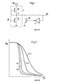
- FIG. 1 The simplest example of an E/D type inverter having a hysteresis characteristic in which a depletion type MOS transistor is used as a load and an enhancement type MOS transistor is used as a driving transistor, is illustrated in Fig. 1.
- the circuit shown in Fig. 1 comprises a logic section 1 in which an enhancement type MOS transistor (hereinafter abbreviated as E MOST) Q 1 is connected between an output node 5 and the ground as a driving transistor for receiving a signal at an input terminal IN and a depletion type MOS transistor Q 2 having its gate connected to the output node 5 is included as a load transistor, an E MOST Q 3 connected in parallel to the E MOST Q 1 , and an inverter 4 having its input connected to the output node 5 and its output connected to the gate of the E MOST Q 3 .
- a hysteresis characteristic is generated by driving the E MOST Q 3 by an output signal of the inverter 4, that is, by an inverted signal of the output of the logic section 1.
- a ratio R DQ 1 /DQ 2 of a driving capability DQ 1 of the E MOST Q 1 versus a driving capability DQ 2 of the D MOST Q 2 .
- the driving capability DQ 1 of the E MOST Q 1 and the driving capability DQ2 of the D MOST Q 2 are proportional to a square of a difference between the gate-source voltage V GS of each transistor and a threshold value V T of the transistor, i.e. (V GS -V T ) 2 , and also it is proportional to a mutual conductance G m (a current amplification factor) that is inherently possessed by each transistor.
- MOS transistors have a large fluctuation in characteristics such as a threshold voltage and a current amplification factor, (G ) and in the case of employing two types of, that is an enhancement type and a depletion type of transistors, the respective types of transistors have fluctuations independently of each other, and therefore, the fluctuation in characteristics of the E/D type inverter would become considerably large. Consequently, with a hysteresis circuit as used in the prior art inverter, the hysteresis characteristic of the inverter was liable to be influenced by the fluctuation of the transistor characteristics, and hence optimum design was difficult.
- G current amplification factor
- the threshold V T of the D MOST Q 2 is lowered or its G m becomes large, the falling curve of the output voltage V OUT would change as shown by a dash line curve A.
- the threshold V T of the E MOST's Q 1 and Q 3 becomes small and their G m becomes large, the rising curve of the output voltage V OUT would be deviated as shown by a dash line curve B. Accordingly, it was difficult to obtain a desired hysteresis characteristic.
- FIG. 4 A first preferred embodiment will be described with reference Fig. 4. This embodiment is constructed by employing a series circuit of an E MOST Q 3 ' and a D MOST Q 4 in place of the feedback control E MOST Q 3 in Fig. 1.
- a D MOST Q 2 serving as a load transistor
- an E MOST Q 1 whose gate is connected to an input terminal IN, and thereby a logic section is formed.
- a circuit for realizing a hysteresis characteristic is formed by an E MOST Q 3 ' having one of its source and drain connected to the node 5, a D MOST Q 4 connected between the other of the source and drain of the E MOST Q 3 and the ground and having its gate grounded, and an inverter 4 having its input connected to the node 5 and its output connected to the gate of the E MOST Q 3 '.
- D MOST Q 4 is connected to its source or drain so as to operate as a constant current source.
- threshold voltages of E MOST Q 1 and Q 3 ' are the same to each other and threshold voltage of D MOSTs Q 2 and Q 4 are the same.
- the EMOST's Q 1 and Q 3 ' are formed through the same process, and the D MOST's Q 2 and Q 42 are formed through the same process.
- the inverter 4 has a circuit structure shown in Fig. 5 in which E MOST Q 41 receiving a signal from the terminal OUT at its gate and a load E MOST Q 42 are connected in series between the terminal V cc and the ground.
- the driving capability ratio of the series circuit consisting of the E MOST Q 3 ' and the D MOST Q 4 to the D MOST Q 2 serving as a load transistor can be easily maintained at a desired value.
- the D MOST Q 4 since the D MOST Q 4 is connected in series with the E MOST Q 3 ', the capability of the driving side (Q 4 , Q 3 ') which operates in response to a feedback signal also varies in proportion to the capability of the load side (Q 2 ), so that the capability ratio of the load side to the driving side can be maintained constant, and thereby the influence of the variation of characteristics of the depletion transistors can be made small.
- an E MOST Q 5 connected between the power supply terminal V cc and the node 5 is further added to the preferred embodiment shown in Fig. 4, and this E MOST Q 5 is driven by an inverter 7 whose input is connected to the output of the inverter 4.
- the function of the E MOST Q S is that the capability of the load side is compensated in reponse to fluctuations in the characteristics of the driving side E MOST Q 1 according to the same principle as the D MOST Q 4 in the first preferred embodiment, and thereby the influence of the characteristics various among the E MOST's can be removed.
- a third preferred embodiment of the present invention will be described with reference to Fig. 7.
- This embodiment is formed by interchanging the sequence of connection of the D MOST Q 4 and the E MOST Q 3 in the preferred embodiment shown in Fig. 4. More particularly, one of the source and drain of the D MOST Q 4 is connected to the node 5 and its gate is connected to the other of the source and drain.
- E MOST Q 3 ' is connected between the other of the source and drain of the D MOST Q 4 and the ground and its gate is connected to an output of an inverter 4.
- a relativity of a driving capability of the series circuit consisting the D MOST 0 4 and the E MOST Q 3 ' to the D MOST Q 2 can be assused, and therefore, a desired hysteresis characteristic can be obtained.
- FIG. 8 A fourth preferred embodiment of the present invention is illustrated in Fig. 8. This embodiment is constructed by replacing the E MOST Q 1 as a driving transistor in Fig. 4, with EMOSTs Q 1A , Q lB and Q 1C forming multi-inputs logic function. Namely, multi-input logic INA ⁇ INB+INC is produced by E MOSTs Q 1A , Q lB and Q 1C . In this embodiment also, an excellent hysteresis characteristic can be obtained similarly to the above-described embodiments.
- an inverter having a hysteresis characteristic that is hardly influenced by fluctuations in the characteristics of transistors can be constructed.
- the present invention is not Limited to an inverter, but it is quite equally applicable to the case where any arbitrary multi-input logic circuit such as NOR, NAND, etc. is used as the logic section, for instance, by replacing a plurality of driving E MOST's for the E MOST Q 1 .
Landscapes
- Engineering & Computer Science (AREA)
- Power Engineering (AREA)
- Physics & Mathematics (AREA)
- Computer Hardware Design (AREA)
- Computing Systems (AREA)
- General Engineering & Computer Science (AREA)
- Mathematical Physics (AREA)
- Logic Circuits (AREA)
Applications Claiming Priority (2)
| Application Number | Priority Date | Filing Date | Title |
|---|---|---|---|
| JP19914/82 | 1982-02-10 | ||
| JP57019914A JPS58137331A (ja) | 1982-02-10 | 1982-02-10 | インバ−タ回路 |
Publications (2)
| Publication Number | Publication Date |
|---|---|
| EP0085991A2 true EP0085991A2 (de) | 1983-08-17 |
| EP0085991A3 EP0085991A3 (de) | 1984-06-20 |
Family
ID=12012477
Family Applications (1)
| Application Number | Title | Priority Date | Filing Date |
|---|---|---|---|
| EP83101284A Ceased EP0085991A3 (de) | 1982-02-10 | 1983-02-10 | Logische Schaltung |
Country Status (3)
| Country | Link |
|---|---|
| US (1) | US4553045A (de) |
| EP (1) | EP0085991A3 (de) |
| JP (1) | JPS58137331A (de) |
Cited By (2)
| Publication number | Priority date | Publication date | Assignee | Title |
|---|---|---|---|---|
| EP0271331A3 (de) * | 1986-12-09 | 1989-05-24 | Kabushiki Kaisha Toshiba | Integrierte Halbleiterschaltung |
| WO2008087015A3 (de) * | 2007-01-16 | 2008-09-18 | Atmel Germany Gmbh | Integrierter schaltkreis |
Families Citing this family (13)
| Publication number | Priority date | Publication date | Assignee | Title |
|---|---|---|---|---|
| US4767947A (en) * | 1983-08-31 | 1988-08-30 | Texas Instruments Incorporated | Constant pulse width generator |
| JPS61161823A (ja) * | 1985-01-10 | 1986-07-22 | Nec Corp | 入力回路 |
| JPH0720060B2 (ja) * | 1985-08-14 | 1995-03-06 | 株式会社東芝 | 出力回路装置 |
| US4728827A (en) * | 1986-12-03 | 1988-03-01 | Advanced Micro Devices, Inc. | Static PLA or ROM circuit with self-generated precharge |
| JP2628942B2 (ja) * | 1990-11-06 | 1997-07-09 | 三菱電機株式会社 | プルアップ抵抗コントロール入力回路及び出力回路 |
| JP2583684B2 (ja) * | 1990-11-06 | 1997-02-19 | 三菱電機株式会社 | プルダウン抵抗コントロール入力回路及び出力回路 |
| US5554942A (en) * | 1995-03-13 | 1996-09-10 | Motorola Inc. | Integrated circuit memory having a power supply independent input buffer |
| US5656957A (en) * | 1995-10-19 | 1997-08-12 | Sgs-Thomson Microelectronics, Inc. | Comparator circuit with hysteresis |
| US5945852A (en) * | 1998-03-31 | 1999-08-31 | Motorola, Inc. | CMOS comparator output circuit with high gain and hysteresis |
| US7187227B2 (en) * | 2002-08-07 | 2007-03-06 | Nippon Telegraph And Telephone Corporation | Driver circuit |
| NL1028142C2 (nl) * | 2005-01-28 | 2006-07-31 | Stork Pmt | Transportinrichting voor geslacht gevogelte. |
| EP4064349A1 (de) | 2013-11-15 | 2022-09-28 | Texas Instruments Incorporated | Verfahren und schaltung zum steuern eines abreicherungstransistors |
| JP2022083085A (ja) * | 2020-11-24 | 2022-06-03 | 株式会社東芝 | 半導体集積回路 |
Family Cites Families (5)
| Publication number | Priority date | Publication date | Assignee | Title |
|---|---|---|---|---|
| US4080539A (en) * | 1976-11-10 | 1978-03-21 | Rca Corporation | Level shift circuit |
| US4071784A (en) * | 1976-11-12 | 1978-01-31 | Motorola, Inc. | MOS input buffer with hysteresis |
| US4097772A (en) * | 1977-06-06 | 1978-06-27 | Motorola, Inc. | MOS switch with hysteresis |
| US4268764A (en) * | 1979-05-01 | 1981-05-19 | Motorola, Inc. | Zero crossover detector |
| JPS5783930A (en) * | 1980-11-12 | 1982-05-26 | Fujitsu Ltd | Buffer circuit |
-
1982
- 1982-02-10 JP JP57019914A patent/JPS58137331A/ja active Pending
-
1983
- 1983-02-10 US US06/465,392 patent/US4553045A/en not_active Expired - Fee Related
- 1983-02-10 EP EP83101284A patent/EP0085991A3/de not_active Ceased
Cited By (4)
| Publication number | Priority date | Publication date | Assignee | Title |
|---|---|---|---|---|
| EP0271331A3 (de) * | 1986-12-09 | 1989-05-24 | Kabushiki Kaisha Toshiba | Integrierte Halbleiterschaltung |
| WO2008087015A3 (de) * | 2007-01-16 | 2008-09-18 | Atmel Germany Gmbh | Integrierter schaltkreis |
| US7683655B2 (en) | 2007-01-16 | 2010-03-23 | Atmel Automotive Gmbh | Integrated circuit |
| DE112008000041B4 (de) | 2007-01-16 | 2023-11-16 | Atmel Corp. | Integrierter Schaltkreis |
Also Published As
| Publication number | Publication date |
|---|---|
| US4553045A (en) | 1985-11-12 |
| EP0085991A3 (de) | 1984-06-20 |
| JPS58137331A (ja) | 1983-08-15 |
Similar Documents
| Publication | Publication Date | Title |
|---|---|---|
| US4553045A (en) | Logic circuit with improved hysteresis characteristics | |
| US4996443A (en) | Integrated circuit for level shift | |
| US6249169B1 (en) | Transistor output circuit | |
| US5352935A (en) | Semiconductor integrated circuit device with internal voltage controlling circuit | |
| US6683445B2 (en) | Internal power voltage generator | |
| US4380710A (en) | TTL to CMOS Interface circuit | |
| US5180965A (en) | Direct-current power source circuit with back gate control circuit for power MOS-FET | |
| US4547749A (en) | Voltage and temperature compensated FET ring oscillator | |
| US4786824A (en) | Input signal level detecting circuit | |
| EP0193901B1 (de) | Komparatorschaltung mit verbesserten Ausgangseigenschaften | |
| US4135125A (en) | Constant voltage circuit comprising an IGFET and a transistorized inverter circuit | |
| US4071784A (en) | MOS input buffer with hysteresis | |
| US5327072A (en) | Regulating circuit for a substrate bias voltage generator | |
| KR100220656B1 (ko) | 입력버퍼회로 | |
| US4446383A (en) | Reference voltage generating circuit | |
| US5180938A (en) | Signal delay circuit having specified transistor threshold levels | |
| US4256974A (en) | Metal oxide semiconductor (MOS) input circuit with hysteresis | |
| US6359814B1 (en) | Negative output voltage charge pump and method therefor | |
| US4700124A (en) | Current and frequency controlled voltage regulator | |
| EP0055570A2 (de) | Logikschaltung | |
| US4626713A (en) | Trip-point clamping circuit for a semiconductor device | |
| US6008679A (en) | Semiconductor integrated circuit and semiconductor input system | |
| US4596939A (en) | Schmitt trigger input gate having delayed feedback for pulse width discrimination | |
| US5648734A (en) | Buffer circuit and bias circuit | |
| EP0361792B1 (de) | Halbleitereinrichtung mit einem eine umgekehrte Vorspannung liefernden Generator |
Legal Events
| Date | Code | Title | Description |
|---|---|---|---|
| PUAI | Public reference made under article 153(3) epc to a published international application that has entered the european phase |
Free format text: ORIGINAL CODE: 0009012 |
|
| AK | Designated contracting states |
Designated state(s): DE FR GB |
|
| RAP1 | Party data changed (applicant data changed or rights of an application transferred) |
Owner name: NEC CORPORATION |
|
| PUAL | Search report despatched |
Free format text: ORIGINAL CODE: 0009013 |
|
| AK | Designated contracting states |
Designated state(s): DE FR GB |
|
| 17P | Request for examination filed |
Effective date: 19840601 |
|
| STAA | Information on the status of an ep patent application or granted ep patent |
Free format text: STATUS: THE APPLICATION HAS BEEN REFUSED |
|
| 18R | Application refused |
Effective date: 19870419 |
|
| RIN1 | Information on inventor provided before grant (corrected) |
Inventor name: MUROTANI, TATSUNORI |