EP0086334A1 - Schaltung zur Änderung des Tastverhältnisses - Google Patents
Schaltung zur Änderung des Tastverhältnisses Download PDFInfo
- Publication number
- EP0086334A1 EP0086334A1 EP83100238A EP83100238A EP0086334A1 EP 0086334 A1 EP0086334 A1 EP 0086334A1 EP 83100238 A EP83100238 A EP 83100238A EP 83100238 A EP83100238 A EP 83100238A EP 0086334 A1 EP0086334 A1 EP 0086334A1
- Authority
- EP
- European Patent Office
- Prior art keywords
- transistor
- current source
- conversion circuit
- pulse duty
- duty conversion
- Prior art date
- Legal status (The legal status is an assumption and is not a legal conclusion. Google has not performed a legal analysis and makes no representation as to the accuracy of the status listed.)
- Granted
Links
- 238000006243 chemical reaction Methods 0.000 title claims description 32
- 239000003990 capacitor Substances 0.000 claims abstract description 19
- 238000010586 diagram Methods 0.000 description 3
- 230000009977 dual effect Effects 0.000 description 3
Images
Classifications
-
- H—ELECTRICITY
- H03—ELECTRONIC CIRCUITRY
- H03K—PULSE TECHNIQUE
- H03K5/00—Manipulating of pulses not covered by one of the other main groups of this subclass
- H03K5/156—Arrangements in which a continuous pulse train is transformed into a train having a desired pattern
- H03K5/1565—Arrangements in which a continuous pulse train is transformed into a train having a desired pattern the output pulses having a constant duty cycle
-
- H—ELECTRICITY
- H03—ELECTRONIC CIRCUITRY
- H03K—PULSE TECHNIQUE
- H03K3/00—Circuits for generating electric pulses; Monostable, bistable or multistable circuits
- H03K3/01—Details
- H03K3/017—Adjustment of width or dutycycle of pulses
Definitions
- This invention relates to a circuit for converting the duty of a pulse signal.
- pulse duty conversion circuits Various types are known. Generally, a pulse duty conversion circuit consists of many elements and its structure is complex. Thus, such a circuit inevitably becomes large and expensive.
- a pulse duty conversion circuit which comprises: a first current source means for supplying a first electric current; a second current source means for supplying a second electric current; a first transistor whose collector is connected to said first current source means, whose emitter is connected to a reference potential and whose base is connected to receive an input pulse signal; a second transistor whose collector is connected to said first current source means and whose emitter is connected to the reference potential; a third transistor whose base is connected to said second current source.
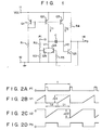
- a pulse duty conversion circuit comprises a first power source terminal 11 and a second power source terminal 12.
- Power source voltage V- is applied to the first power source terminal 11, and a predetermined reference voltage (i.e. ground potential) is applied to the second power source terminal 12.
- the circuit further comprises an input terminal 13 for receiving an input pulse Pi (Fig. 2A) and an output terminal 14 for supplying an output pulse (Fig. 2D).
- a series circuit which consists of a PNP transistor Ql and a resistor Rl.
- the base and collector of the transistor Ql are connected to each other.
- the emitter of the transistor Ql is connected to the first power source terminal 11, and the base and the collector of the transistor Ql are connected to the second power source terminal 12 through the resistor Rl.
- Two PNP transistors Q2 and Q3 are provided which are current mirror circuits to the transistor Ql. That is, the bases of these transistors Q2 and Q3 are connected to the base of the transistor Ql, and the emitters of these transistors Q2 and Q3 are connected to the first power source terminal 11.
- a series circuit of resistors R2 and R3 is connected for applying a bias voltage.
- the junction of the resistors R2 and R3 is connected to the base of an NPN transistor Q4.
- the emitter of the transistor Q4 is connected to the ground potential, and the collector of the transistor Q4 is connected to the collector of the transistor Q2 and to the base of an NPN transistor Q5 via a capacitor C.
- the emitter of the transistor Q5 is connected to the reference voltage (i.e. ground potential).
- the collector of the transistor Q5 is connected to the output terminal 14 and also to the first power source terminal 11 through a load resistor R4.
- the collector of the transistor Q5 is also connected to the base of an NPN transistor Q6 through the load resistor R5.
- the load resistor R4 may be replaced by an impedance circuit.
- the collector of the transistor Q5 is connected to the collector of the transistor Q2, and the emitter of the transistor Q2 is connected to the second power source terminal 12.
- a pulse signal Pi consisting of pulses generated at intervals T (Fig. 2A) is supplied to the input terminal 11. While the potential of the signal Pi remains at a high level ("1" level), that is, for the duration of a positive input pulse, the transistor Q4 is on and its collector potential V 1 falls to ground potential (i.e., zero potential) as shown in Fig. 2B. When the transistor Q4 is turned on, the electric charge in the capacitor C is instantaneously discharged via the transistor Q4. The base potential V 2 of the transistor Q5 then abruptly falls as shown in Fig. 2C. The transistor Q5 is thus turned off. A voltage is applied from the first power source terminal 11 through the resistors R4 and R5 to the base of the transistor Q6.
- the output pulse signal Po has a potential which is determined by the voltage division ratio with which the resistors R4 and R5 divide the power source voltage V CC , said potential being a high level ("1" level).
- the transistors Q5 and Q6 are turned off and on, current I 2 starts flowing from the transistor Q3 to the transistor Q6 through the capacitor C.
- the capacitor C therefore accumulates an electric charge, and the base potential V 2 of the transistor Q5 rises.
- the base potential V 2 reaches the base-emitter threshold voltage V BET of the transistor Q5
- the transistor Q5 is turned on.
- the potential of the transistor Q5, i.e. the potential of the output terminal 14 falls to ground potential. Consequently, the transistor Q6 is turned off.
- the potential of the output pulse signal Po is at a low level ("0" level).
- the potential difference ⁇ V 2 between the ends of the capacitor C is given by: I 2 ⁇ t 2 /C.
- the charging period t l is longer than the duration of the positive pulse of the input pulse signal Pi. Hence, within the charging period t 2 the potential of the input terminal 13 falls to ground potential and the transistor Q4 is turned off.
- the capacitor C starts accumulating current In and is thus electrically charged opposite to the polarity with which it is charged when it accumulates current I 2 .
- the collector potentials of the transistors Q4 and Q6 rise.
- the next positive pulse of the input pulse signal Pi is applied to the input terminal 13
- the transistor Q4 is turned on, and the electric charge is discharged from the capacitor C through the transistor Q4.
- the base potential of the transistor Q4 instantaneously falls.
- the elements of the circuit operate in the same manner as when the first positive pulse is supplied to the input terminal 13. If the capacitor C is electrically charged for only a period t 1 , the potential difference ⁇ V 1 between the ends of the capacitor C is given as: I 1 ⁇ t 1 /C.
- the duty cycle of the output pulse signal Po can be other than 50% if I 1 is not equal to I 2 .
- the duty cycle of the output pulse signal Po can be of any desired value only if currents I 1 and I 2 are different and the ratio of current I 1 to current I 2 has a proper value.
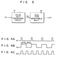
- Fig. 3 is a block diagram of a doubler circuit which is provided with the pulse duty conversion circuit shown in Fig. 1.
- Figs. 4A through 4C are timing charts of the signals supplied to various elements of the circuit shown in Fig. 3.
- the pulse duty conversion circuit 31 is designed to convert an input pulse signal into a pulse signal whose duty is 50%.
- the doubler circuit further comprises a monostable multivibrator 32 of dual trigger type.
- the multivibrator 32 is designed to receive an output pulse signal Po from the pulse duty conversion circuit 31 and generate two pulses as each pulse of the signal Po rises and falls. -
- the pulse duty conversion circuit 31 When an input pulse signal Pi, such as is shown in Fig. 4A, is supplied to the pulse duty conversion circuit 31, the circuit 31 generates an output pulse signal Po which is shown in Fig. 4B and whose duty is 50%.
- the pulse signal Po is supplied to the multivibrator 32.
- the multivibrator 32 generates two pulses in synchronism with the leading edge and trailing edge of each pulse of the signal Po. Therefore, it generates such a pulse signal Pf as shown in Fig. 4C. As evident from Figs. 4A, 4B and 4C, the pulse signal Pf has a frequency twice that of the input pulse signal Pi (Fig. 4A).
- the present invention is not limited to the embodiment described above.
- the current source circuit consisting of the transistors Ql, Q2 and Q3 and the resistor Rl may be replaced by any other circuit that can determine any desired ratio of the current I I to the current I 2 .
- the reference potential may be other than the ground potential, so far as it is lower than the power source potential V CC .
- the NPN transistors used in the embodiment may be replaced by PNP transistors and the PNP transistors used in the embodiment may be replaced by NPN transistors. If this is the case, the power source potential V CC and the reference potential will, of course, be interchanged.
- the pulse duty conversion circuit comprises only a few transistors Q4, Q5 and Q6, only one capacitor C and only two resistors R4 and R5, besides a current source circuit consisting of transistors Ql, Q2 and Q3 and a resistor Rl. Its structure is simple. Yet it can convert an input pulse signal into a pulse signal of any desired pulse duty merely by changing the ratio of the current I 1 to the current I 2 . If the pulse duty conversion circuit is combined with a monostable multivibrator of dual trigger type, its pulse duty is set to 50% and its output pulse signal is supplied to the multivibrator, a doubler circuit with a simple structure will be provided.
Landscapes
- Physics & Mathematics (AREA)
- Nonlinear Science (AREA)
- Pulse Circuits (AREA)
- Manipulation Of Pulses (AREA)
Applications Claiming Priority (2)
| Application Number | Priority Date | Filing Date | Title |
|---|---|---|---|
| JP1231782A JPS58130616A (ja) | 1982-01-28 | 1982-01-28 | デユ−テイ変換回路 |
| JP12317/82 | 1982-01-28 |
Publications (2)
| Publication Number | Publication Date |
|---|---|
| EP0086334A1 true EP0086334A1 (de) | 1983-08-24 |
| EP0086334B1 EP0086334B1 (de) | 1986-07-02 |
Family
ID=11801931
Family Applications (1)
| Application Number | Title | Priority Date | Filing Date |
|---|---|---|---|
| EP83100238A Expired EP0086334B1 (de) | 1982-01-28 | 1983-01-13 | Schaltung zur Änderung des Tastverhältnisses |
Country Status (3)
| Country | Link |
|---|---|
| EP (1) | EP0086334B1 (de) |
| JP (1) | JPS58130616A (de) |
| DE (1) | DE3364287D1 (de) |
Cited By (2)
| Publication number | Priority date | Publication date | Assignee | Title |
|---|---|---|---|---|
| AU572758B2 (en) * | 1984-06-11 | 1988-05-12 | Nec Corporation | Pulse oscillator |
| CN104242875B (zh) * | 2013-06-19 | 2017-07-04 | 成都振芯科技股份有限公司 | 单转双占空比可调电路 |
Families Citing this family (1)
| Publication number | Priority date | Publication date | Assignee | Title |
|---|---|---|---|---|
| JPS6193714A (ja) * | 1984-10-12 | 1986-05-12 | Toshiba Corp | デユ−テイ変換回路 |
Citations (8)
| Publication number | Priority date | Publication date | Assignee | Title |
|---|---|---|---|---|
| GB916630A (en) * | 1959-03-13 | 1963-01-23 | Nat Res Dev | Improvements in or relating to transistor timing circuits |
| GB1107629A (en) * | 1965-06-25 | 1968-03-27 | Standard Telephones Cables Ltd | A monostable multivibrator giving a constant mark to space ratio |
| DE2022548A1 (de) * | 1969-05-08 | 1970-12-23 | Marconi Co Ltd | Triggerbare monostabile Schaltung |
| US3590283A (en) * | 1969-05-15 | 1971-06-29 | Bell Telephone Labor Inc | Regenerative switching circuits employing charge storage diodes |
| US3711729A (en) * | 1971-08-04 | 1973-01-16 | Burroughs Corp | Monostable multivibrator having output pulses dependent upon input pulse widths |
| US3712993A (en) * | 1971-11-23 | 1973-01-23 | Gen Motors Corp | Pulse length multiplier circuit |
| US3770987A (en) * | 1972-03-30 | 1973-11-06 | Litton Business Systems Inc | Extended range capacitive timing circuit |
| US4140928A (en) * | 1976-06-14 | 1979-02-20 | Trio Kabushiki Kaisha | Monostable multivibrator |
-
1982
- 1982-01-28 JP JP1231782A patent/JPS58130616A/ja active Granted
-
1983
- 1983-01-13 DE DE8383100238T patent/DE3364287D1/de not_active Expired
- 1983-01-13 EP EP83100238A patent/EP0086334B1/de not_active Expired
Patent Citations (8)
| Publication number | Priority date | Publication date | Assignee | Title |
|---|---|---|---|---|
| GB916630A (en) * | 1959-03-13 | 1963-01-23 | Nat Res Dev | Improvements in or relating to transistor timing circuits |
| GB1107629A (en) * | 1965-06-25 | 1968-03-27 | Standard Telephones Cables Ltd | A monostable multivibrator giving a constant mark to space ratio |
| DE2022548A1 (de) * | 1969-05-08 | 1970-12-23 | Marconi Co Ltd | Triggerbare monostabile Schaltung |
| US3590283A (en) * | 1969-05-15 | 1971-06-29 | Bell Telephone Labor Inc | Regenerative switching circuits employing charge storage diodes |
| US3711729A (en) * | 1971-08-04 | 1973-01-16 | Burroughs Corp | Monostable multivibrator having output pulses dependent upon input pulse widths |
| US3712993A (en) * | 1971-11-23 | 1973-01-23 | Gen Motors Corp | Pulse length multiplier circuit |
| US3770987A (en) * | 1972-03-30 | 1973-11-06 | Litton Business Systems Inc | Extended range capacitive timing circuit |
| US4140928A (en) * | 1976-06-14 | 1979-02-20 | Trio Kabushiki Kaisha | Monostable multivibrator |
Non-Patent Citations (1)
| Title |
|---|
| PATANT ABSTRACTS OF JAPAN, vol. 3, no. 22, 24 February 1979, page 116 E93; JP-A-54 000 958 * |
Cited By (2)
| Publication number | Priority date | Publication date | Assignee | Title |
|---|---|---|---|---|
| AU572758B2 (en) * | 1984-06-11 | 1988-05-12 | Nec Corporation | Pulse oscillator |
| CN104242875B (zh) * | 2013-06-19 | 2017-07-04 | 成都振芯科技股份有限公司 | 单转双占空比可调电路 |
Also Published As
| Publication number | Publication date |
|---|---|
| EP0086334B1 (de) | 1986-07-02 |
| JPS58130616A (ja) | 1983-08-04 |
| JPH0344459B2 (de) | 1991-07-08 |
| DE3364287D1 (en) | 1986-08-07 |
Similar Documents
| Publication | Publication Date | Title |
|---|---|---|
| US4052623A (en) | Isolated semiconductor gate control circuit | |
| US4652774A (en) | Rectangular wave-shaping circuit with varying threshold level | |
| US4054804A (en) | Bipolar charging and discharging circuit | |
| US3031583A (en) | Stairstep waveform generator | |
| EP0086334B1 (de) | Schaltung zur Änderung des Tastverhältnisses | |
| US4358689A (en) | Analog to digital interface circuit | |
| EP0401911B1 (de) | Schaltungsanordnung | |
| GB2072446A (en) | Oscillator circuit | |
| US3961207A (en) | Output retaining electronic circuit | |
| US4256981A (en) | Circuit arrangement for generating a pulse with a delayed edge | |
| EP0272924A2 (de) | Pulsgenerator | |
| US3793540A (en) | Constant current source for time delay device | |
| SU1205264A1 (ru) | Генератор напр жени треугольной формы | |
| JPS5826850B2 (ja) | アステ−ブルマルチバイブレ−タ | |
| JPH02690Y2 (de) | ||
| SU1182633A1 (ru) | Генератор импульсов | |
| EP0132591B1 (de) | Impulsgeneratorschaltung | |
| JPS6311768Y2 (de) | ||
| SU1251297A1 (ru) | Генератор импульсов | |
| SU1193781A1 (ru) | Генератор импульсов | |
| JPH0414533B2 (de) | ||
| JPH057778Y2 (de) | ||
| SU1205047A1 (ru) | Преобразователь временного интервала между импульсами в посто нный ток | |
| JPS57166735A (en) | Driving circuit | |
| KR790002073Y1 (ko) | 펄스폭 변조기 |
Legal Events
| Date | Code | Title | Description |
|---|---|---|---|
| PUAI | Public reference made under article 153(3) epc to a published international application that has entered the european phase |
Free format text: ORIGINAL CODE: 0009012 |
|
| PUAI | Public reference made under article 153(3) epc to a published international application that has entered the european phase |
Free format text: ORIGINAL CODE: 0009012 |
|
| 17P | Request for examination filed |
Effective date: 19830113 |
|
| AK | Designated contracting states |
Designated state(s): DE FR GB |
|
| RAP1 | Party data changed (applicant data changed or rights of an application transferred) |
Owner name: KABUSHIKI KAISHA TOSHIBA |
|
| GRAA | (expected) grant |
Free format text: ORIGINAL CODE: 0009210 |
|
| AK | Designated contracting states |
Kind code of ref document: B1 Designated state(s): DE FR GB |
|
| ET | Fr: translation filed | ||
| REF | Corresponds to: |
Ref document number: 3364287 Country of ref document: DE Date of ref document: 19860807 |
|
| PLBE | No opposition filed within time limit |
Free format text: ORIGINAL CODE: 0009261 |
|
| STAA | Information on the status of an ep patent application or granted ep patent |
Free format text: STATUS: NO OPPOSITION FILED WITHIN TIME LIMIT |
|
| 26N | No opposition filed | ||
| PGFP | Annual fee paid to national office [announced via postgrant information from national office to epo] |
Ref country code: GB Payment date: 19980105 Year of fee payment: 16 |
|
| PGFP | Annual fee paid to national office [announced via postgrant information from national office to epo] |
Ref country code: FR Payment date: 19980109 Year of fee payment: 16 |
|
| PGFP | Annual fee paid to national office [announced via postgrant information from national office to epo] |
Ref country code: DE Payment date: 19980116 Year of fee payment: 16 |
|
| PG25 | Lapsed in a contracting state [announced via postgrant information from national office to epo] |
Ref country code: GB Free format text: LAPSE BECAUSE OF NON-PAYMENT OF DUE FEES Effective date: 19990113 |
|
| GBPC | Gb: european patent ceased through non-payment of renewal fee |
Effective date: 19990113 |
|
| PG25 | Lapsed in a contracting state [announced via postgrant information from national office to epo] |
Ref country code: FR Free format text: LAPSE BECAUSE OF NON-PAYMENT OF DUE FEES Effective date: 19990930 |
|
| PG25 | Lapsed in a contracting state [announced via postgrant information from national office to epo] |
Ref country code: DE Free format text: LAPSE BECAUSE OF NON-PAYMENT OF DUE FEES Effective date: 19991103 |
|
| REG | Reference to a national code |
Ref country code: FR Ref legal event code: ST |