EP0086961A2 - Plaquette multicouche pour l'interconnexion de circuits grande vitesse - Google Patents
Plaquette multicouche pour l'interconnexion de circuits grande vitesse Download PDFInfo
- Publication number
- EP0086961A2 EP0086961A2 EP83100521A EP83100521A EP0086961A2 EP 0086961 A2 EP0086961 A2 EP 0086961A2 EP 83100521 A EP83100521 A EP 83100521A EP 83100521 A EP83100521 A EP 83100521A EP 0086961 A2 EP0086961 A2 EP 0086961A2
- Authority
- EP
- European Patent Office
- Prior art keywords
- board
- conductive
- conductive layer
- paths
- holes
- Prior art date
- Legal status (The legal status is an assumption and is not a legal conclusion. Google has not performed a legal analysis and makes no representation as to the accuracy of the status listed.)
- Withdrawn
Links
Images

Classifications
-
- H—ELECTRICITY
- H05—ELECTRIC TECHNIQUES NOT OTHERWISE PROVIDED FOR
- H05K—PRINTED CIRCUITS; CASINGS OR CONSTRUCTIONAL DETAILS OF ELECTRIC APPARATUS; MANUFACTURE OF ASSEMBLAGES OF ELECTRICAL COMPONENTS
- H05K5/00—Casings, cabinets or drawers for electric apparatus
-
- H—ELECTRICITY
- H05—ELECTRIC TECHNIQUES NOT OTHERWISE PROVIDED FOR
- H05K—PRINTED CIRCUITS; CASINGS OR CONSTRUCTIONAL DETAILS OF ELECTRIC APPARATUS; MANUFACTURE OF ASSEMBLAGES OF ELECTRICAL COMPONENTS
- H05K3/00—Apparatus or processes for manufacturing printed circuits
- H05K3/46—Manufacturing multilayer circuits
- H05K3/4611—Manufacturing multilayer circuits by laminating two or more circuit boards
- H05K3/4641—Manufacturing multilayer circuits by laminating two or more circuit boards having integrally laminated metal sheets or special power cores
-
- H—ELECTRICITY
- H05—ELECTRIC TECHNIQUES NOT OTHERWISE PROVIDED FOR
- H05K—PRINTED CIRCUITS; CASINGS OR CONSTRUCTIONAL DETAILS OF ELECTRIC APPARATUS; MANUFACTURE OF ASSEMBLAGES OF ELECTRICAL COMPONENTS
- H05K3/00—Apparatus or processes for manufacturing printed circuits
- H05K3/22—Secondary treatment of printed circuits
- H05K3/222—Completing of printed circuits by adding non-printed jumper connections
-
- H—ELECTRICITY
- H05—ELECTRIC TECHNIQUES NOT OTHERWISE PROVIDED FOR
- H05K—PRINTED CIRCUITS; CASINGS OR CONSTRUCTIONAL DETAILS OF ELECTRIC APPARATUS; MANUFACTURE OF ASSEMBLAGES OF ELECTRICAL COMPONENTS
- H05K1/00—Printed circuits
- H05K1/02—Details
- H05K1/0213—Electrical arrangements not otherwise provided for
- H05K1/0216—Reduction of cross-talk, noise or electromagnetic interference
- H05K1/023—Reduction of cross-talk, noise or electromagnetic interference using auxiliary mounted passive components or auxiliary substances
- H05K1/0231—Capacitors or dielectric substances
-
- H—ELECTRICITY
- H05—ELECTRIC TECHNIQUES NOT OTHERWISE PROVIDED FOR
- H05K—PRINTED CIRCUITS; CASINGS OR CONSTRUCTIONAL DETAILS OF ELECTRIC APPARATUS; MANUFACTURE OF ASSEMBLAGES OF ELECTRICAL COMPONENTS
- H05K1/00—Printed circuits
- H05K1/02—Details
- H05K1/0286—Programmable, customizable or modifiable circuits
- H05K1/0287—Programmable, customizable or modifiable circuits having an universal lay-out, e.g. pad or land grid patterns or mesh patterns
-
- H—ELECTRICITY
- H05—ELECTRIC TECHNIQUES NOT OTHERWISE PROVIDED FOR
- H05K—PRINTED CIRCUITS; CASINGS OR CONSTRUCTIONAL DETAILS OF ELECTRIC APPARATUS; MANUFACTURE OF ASSEMBLAGES OF ELECTRICAL COMPONENTS
- H05K1/00—Printed circuits
- H05K1/16—Printed circuits incorporating printed electric components, e.g. printed resistors, capacitors or inductors
- H05K1/162—Printed circuits incorporating printed electric components, e.g. printed resistors, capacitors or inductors incorporating printed capacitors
-
- H—ELECTRICITY
- H05—ELECTRIC TECHNIQUES NOT OTHERWISE PROVIDED FOR
- H05K—PRINTED CIRCUITS; CASINGS OR CONSTRUCTIONAL DETAILS OF ELECTRIC APPARATUS; MANUFACTURE OF ASSEMBLAGES OF ELECTRICAL COMPONENTS
- H05K2201/00—Indexing scheme relating to printed circuits covered by H05K1/00
- H05K2201/01—Dielectrics
- H05K2201/0183—Dielectric layers
- H05K2201/0191—Dielectric layers wherein the thickness of the dielectric plays an important role
-
- H—ELECTRICITY
- H05—ELECTRIC TECHNIQUES NOT OTHERWISE PROVIDED FOR
- H05K—PRINTED CIRCUITS; CASINGS OR CONSTRUCTIONAL DETAILS OF ELECTRIC APPARATUS; MANUFACTURE OF ASSEMBLAGES OF ELECTRICAL COMPONENTS
- H05K2201/00—Indexing scheme relating to printed circuits covered by H05K1/00
- H05K2201/09—Shape and layout
- H05K2201/09209—Shape and layout details of conductors
- H05K2201/0929—Conductive planes
- H05K2201/09309—Core having two or more power planes; Capacitive laminate of two power planes
-
- H—ELECTRICITY
- H05—ELECTRIC TECHNIQUES NOT OTHERWISE PROVIDED FOR
- H05K—PRINTED CIRCUITS; CASINGS OR CONSTRUCTIONAL DETAILS OF ELECTRIC APPARATUS; MANUFACTURE OF ASSEMBLAGES OF ELECTRICAL COMPONENTS
- H05K2201/00—Indexing scheme relating to printed circuits covered by H05K1/00
- H05K2201/09—Shape and layout
- H05K2201/09209—Shape and layout details of conductors
- H05K2201/095—Conductive through-holes or vias
- H05K2201/09609—Via grid, i.e. two-dimensional array of vias or holes in a single plane
-
- H—ELECTRICITY
- H05—ELECTRIC TECHNIQUES NOT OTHERWISE PROVIDED FOR
- H05K—PRINTED CIRCUITS; CASINGS OR CONSTRUCTIONAL DETAILS OF ELECTRIC APPARATUS; MANUFACTURE OF ASSEMBLAGES OF ELECTRICAL COMPONENTS
- H05K2201/00—Indexing scheme relating to printed circuits covered by H05K1/00
- H05K2201/10—Details of components or other objects attached to or integrated in a printed circuit board
- H05K2201/10227—Other objects, e.g. metallic pieces
- H05K2201/10287—Metal wires as connectors or conductors
-
- H—ELECTRICITY
- H05—ELECTRIC TECHNIQUES NOT OTHERWISE PROVIDED FOR
- H05K—PRINTED CIRCUITS; CASINGS OR CONSTRUCTIONAL DETAILS OF ELECTRIC APPARATUS; MANUFACTURE OF ASSEMBLAGES OF ELECTRICAL COMPONENTS
- H05K2201/00—Indexing scheme relating to printed circuits covered by H05K1/00
- H05K2201/10—Details of components or other objects attached to or integrated in a printed circuit board
- H05K2201/10227—Other objects, e.g. metallic pieces
- H05K2201/10333—Individual female type metallic connector elements
Definitions
- This invention relates to panel boards and socket terminals for mounting electronic components.
- Multilayer panel boards for electronic components have sandwiches of conductive and insulative layers, one conductive layer carrying a voltage and one conductive layer being grounded.
- Wire-wrap socket terminals which are held in mounting holes in the insulative layers, have sockets on one end for insertion of leads of electronic components and posts on the other end for wrapping wire to make connections.
- Doucet (United States Patent No. 4,004,196) discloses a multi-layer wire-wrap panel having three conductive layers and two insulative layers. Portions of the top conductive layer are cut away for mounting wire-wrap socket terminals with their heads flush against the insulative layer but not in contact with the conductive layer.
- Turner et al. United States Patent No. 3,895,435, and D'Aboville, United States Patent No. 3,568,000, disclose plated-through holes for connecting conductive layers of a multi-layer panel.
- the panel sandwich includes a pair of embedded conductive layers with a ground layer between them and two additional ground layers on the exposed surfaces of the sandwich.
- Known panel boards are not suitable, however, for wire-wrapped interconnection of high-speed (e.g., Schottky) logic circuits.
- Such circuits consume more power than the current-carrying capacity of the power lines in typical panels can accommodate.
- the size of the distributed capacitance between the voltage supply source and the ground return in such boards is generally too small to prevent switching signals in such circuits from causing spikes in the power lines.
- the wire leads between the logic circuit and the power terminals produce undesirably high inductance levels.
- the invention features a multilayer panel board having a first electrically conductive layer, for carrying a first voltage, positioned between second and third electrically conductive layers for carrying a different second voltage, and first and second electrically insulative layers separating the first conductive layer from the second and third conductive layers by a distance small enough to produce a large distributed capacitance between the first conductive layer and the second and third conductive layers.
- a fourth electrically conductive layer positioned on the other side of the second conductive layer from the first conductive layer, also carries the first voltage, and is separated from the fourth conductive layer by a third insulating layer; the distance separating the first conductive layer from the second and third conductive layer is between about 0.005 inches (0.127 mm) and about 0.009 inches (0.229 mm); the second voltage is at ground level; the large distributed capacitance is at least 0.02 microfarads; the first and fourth conductive layers are electrically connected by regularly spaced conductive voltage paths, and the second and third conductive layers are electrically connected by regularly spaced conductive ground paths, for increasing the current carrying capacity of the board, decreasing the resistance across the board, maintaining the second voltage uniformly at all points on said second and third conductive layers, and maintaining the first voltage uniformly at all points on said first and fourth conductive layers; the conductive paths are regularly distributed holes through the first, second, third and fourth conductive layers and through the first, second and third insulation layers of the board, with
- the invention features a panel board for holding electrical terminals, having an electrically conductive layer, an electrically insulative layer attached to the electrically conductive layer, the insulative layer having a number of round mounting holes for holding the terminals, the conductive layer having a number of round clearance holes " corresponding to the mounting holes and coaxial with, and of slightly larger diameter than, the corresponding mounting holes, the clearance holes being spaced apart across said board, and the conductive layer extending across the spaces between the clearance holes, whereby inductance of the conductive layer is minimized and contact between the terminals and the conductive layer is prevented.
- the difference in the diameter of each said clearance hole and the corresponding said mounting hole is less than 0.035 inches (0.889 mm).
- the invention features a combination for electrically connecting, without wiring, an electrical terminal mounted on a panel board to an electrically conductive layer of the board, the combination having an electrically insulative layer in the board, the insulative layer having a mounting hole for holding the terminal, a clearance hole in the electrical conductive layer, the clearance hole being coaxial with, and slightly larger than, the mounting hole for normally insulating the terminal from the conductive layer, and an electrically conductive ring connector positioned to electrically connect the terminal directly to the conductive layer.
- the terminal has a shaft held in the mounting hole and a head or wire-wrap post projected beyond the insulative layer and the conductive layer, and the ring is mounted around the head in contact with the head and the conductive layer or around the post in contact with the post and the conductive layer.
- the close spacing of a voltage layer between two ground layers provides a large distributed capacitance (without requiring many discrete isolation capacitors) which inhibits switching signals from causing voltage spikes in the power lines.
- Minimizing the diameters of the holes which must be cut through the voltage and ground layers to clear the mounted terminals improves the uniformity of voltage across each layer, reduces the inductance of the conductive layers, and improves the characteristic impedance of the board for high-frequency applications.
- Electrically tying together the ground layers and the voltage layers at many points distributed across the board assures a uniform voltage level at all points on each voltage layer and a uniform ground at all points on both ground layers, and also doubles the current carrying capacity of, and halves the resistance across, the board.
- the location of the plated-through holes close to the socket terminals enables discrete capacitors to be connected close to mounted integrated circuits.
- the pattern of grounded and powered plated-through holes permits the capacitors to be mounted sideways or lengthwise on the board.
- the close proximity of adjacent columns of socket terminals permits mounting components densely, thereby shortening the interconnection lead lengths.
- the ring connectors enable direct connection of the socket terminals to voltage and ground without using wire wrap connections (which hamper high-speed switching because of the inductance inherent in the lead length and lead wrapping).
- the board is able to handle high-speed logic circuits.
- the socket terminals have large diameter heads, permitting easy insertion of component pins, but the contour of the connecting portion between the terminal head and terminal shaft prevents electrical short-circuit with the voltage layers.
- the top voltage layer or the bottom ground layer can be connected directly to any socket terminal using the ring connectors.
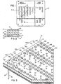
- multilayer panel board 10 has a grid pattern 12 of wire-wrap socket terminals and plated-through holes for mounting and electrically interconnecting conventional integrated circuits contained in dual in-line packages (DIPs) and other components (not shown).
- DIPs dual in-line packages
- board 10 has two copper voltage plates 14, 18 connected to a source of voltage V (not shown) and two copper ground plates 16, 20 connected to ground (not shown).
- Plates 14, 16, 18, 20 are each preferably 0.0027" (0.069 mm) thick (preferred range 0.0025" (0.064 mm) to 0.0029" (0.074 mm)) and are separated (as shown) by three insulative layers 22, 24, 26 of glass epoxy.
- Epoxy layers 24, 26 are thin enough, preferably 0.008" (0.203 mm) thick (preferred range 0.005" (0.127 mm) to 0.009" (0.229 mm)), to establish a large distributed capacitance of about 0.03 microfarads between voltage plate 18 and ground plates 16, 20.
- Epoxy layer 22 is preferably 0.102" (2.591 mm) thick (preferred range 0.100" (2.540 mm) to 0.104" (2.642 mm)).
- voltage plates 14, 18 are electrically connected by plated-through voltage holes 28 (distributed regularly across board 10).
- ground plates 16, 20 are electrically connected by plated-through ground holes 30 (also distributed regularly across board 10). All points on voltage plates 14, 18 are thus held at a uniform voltage V, while all points on ground plates 16, 20 are uniformly grounded.
- the current carrying capacity of the board is doubled and the resistance across the board is halved- - compared with boards having single voltage plates or single ground plates.
- each plated-through voltage hole 28 has a sleeve 40 of copper plating which covers the inside of a hole comprising hole segments 42, 44, 46 in the epoxy and holes 48, 50 in voltage plates 14, 18.
- the diameters of holes 48, 50 preferably 0.041" (1.041 mm) (preferred range 0.039" (0.991 mm) to 0.043" (1.125 mm)), are smaller than the diameters of hole segments 42, 44, 46.
- Holes 52, 54 in ground plates 16, 20 are larger in diameter than hole segments 42, 46 and are preferably 0.087" (2.210 mm) (preferred range 0.085" (2.159 mm) to 0.090" (2.286 mm)).
- Sleeve 40 therefore electrically connects voltage plates 14, 18, but is electrically insulated from ground plates 16, 20.
- the inside hole 56 in sleeve 40 is preferably 0.037" (0.940 mm) in diameter (preferred range 0.034" (0.864 mm) to 0.040" (1.016 mm)).
- the copper plating of sleeve 40 extends across the surface of plate 14 (as shown), where it is approximately 0.003 inches (0.076 mm) thick.
- each plated-through ground hole 30 similarly has copper-plated sleeve 70, which electrically connects ground plates 16, 20, but is electrically insulated from voltage plates 14, 18 (because the diameters of holes 72, 74 are smaller than diameters of hole segments 76, 78, 80, which are in turn small than the diameters of holes 82, 84).
- the copper plating of sleeve 70 extends across the surface of plate 20 (as shown), where it is approximately 0.003 inches (0.076 mm) thick.
- holes 72, 74 are similar to holes 48, 50; holes 82, 84 are similar to holes 52, 54; hole segments 76, 78, 80 are similar to hole segments 46, 44, 42; and hole 86 is similar to hole 56.
- the densities of the plated-through ground holes and plated-through voltage holes are both approximately 4 holes per square inch across board 10.
- grid pattern 12 has a regular arrangement (as shown) of plated-through voltage and ground holes 28, 30, and of wire-wrap socket terminals 118, 120, 122 mounted in holes (not shown) in board 10.
- each wire-wrap socket terminal 130 fabricated of gold-over-nickel-plated, half-hard, yellow brass, has on one end a solid 0.025" (0.635 mm) square post 132 of a selected length (preferred range 0.350" (8.890 mm) to 0.550" (13.970 mm)) to hold wrapped wire for making electrical connections.
- round portion 134 has socket 136 opening to tapered portion 138 for easy insertion of a lead of a DIP or other component.
- Socket head 140 has tapered section 142 which tapers from a diameter of preferably .072" (1.829 mm) (preferred range 0.070" (1.788 mm) to 0.084" (2.134 mm)) to a diameter of preferably .062" (1.575 mm) (preferred range 0.060" (1.524 mm) to 0.064" (1.626 mm)).
- Tapered section 142 ends at flat seat portion 143, which engages the surface of board 10 when terminal 130 is mounted.
- Shaft 144 rests in a hole in board 10 and knurled section 146 assures a tight interference fit in the hole.
- Tapered section 142 allows the use of a large diameter head 40, which enables easier insertion of component leads and pins.
- section 142 can be stepped or have any other contour which precludes a short-circuit between head 40 and plate 14 when terminal 130 is mounted in board 10.
- Each wire-wrap socket terminal 130 is mounted on board 10 in one of three different configurations: universal, grounded and powered. Referring to Figs. 7,
- the densities of the plated-through ground holes and plated-through voltage holes are both approximately 4 holes per square inch across board 10.
- grid pattern 12 has a regular arrangement (as shown) of plated-through voltage and ground holes 28, 30, and of wire-wrap socket terminals 118, 120, 122 mounted in holes (not shown) in board 10.
- each wire-wrap socket terminal 130 fabricated of gold-over-nickel-plated, half-hard, yellow brass, has on one end a solid 0.025" (0.635 mm) square post 132 of a selected length (preferred range 0.350" (8.890 mm) to 0.550" (13.970 mm)) to hold wrapped wire for making electrical connections.
- round portion 134 has socket 136 opening to tapered portion 138 for easy insertion of a lead of a DIP or other component.
- Socket head 140 has tapered section 142 which tapers from a diameter of preferably .072" (1.829 mm) (preferred range 0.070" (1.788 mm) to 0.084" (2.134 mm)) to a diameter of preferably .062" (1.575 mm) (preferred range 0.060" (1.524 mm) to 0.064" (1.626 mm)).
- Tapered section 142 ends at flat seat portion 143, which engages the surface of board 10 when terminal 130 is mounted.
- Shaft 144 rests in a hole in board 10 and knurled section 146 assures a tight interference fit in the hole.
- Tapered section 142 allows the use of a large diameter head140, which enables easier insertion of component leads and pins.
- section 142 can be stepped or have any other contour which precludes a short-circuit between head140 and plate 14 when terminal 130 is mounted in board 10.
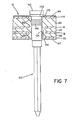
- Each wire-wrap socket terminal 130 is mounted on board 10 in one of three different configurations: universal, grounded and powered. Referring to Figs. 7, 8 and 9, in each of the three mounting configurations zi wire-wrap socket terminal 130 is interference fitted into a hole 154 in board 10.
- hole 154 preferably of diameter 0.056" (1.422 mm) (preferred range 0.055" (1.397 mm) to 0.056" (1.422 mm)) extends through an epoxy section 156 which spans the full thickness of board 10 and insulates terminal 130 from plates 14, 16, 18, 20, into which circular clearance holes 158, preferably of 0.087" (2.210 mm) diameter (preferred range 0.085" (2.159 mm) to 0.089" (2.261 mm)) have been cut before fabrication of board 10.
- Seat portion 143 rests against epoxy section 156 and tapered section 142 prevents head 140 from short-circuiting against plate 14 or plating 145.
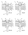
- the grounded mounting configuration is similar to the universal mounting configuration of Fig. 7, except that epoxy section 156 extends only to ground plate 20.
- Plate 20 has hole 160 preferably of diameter 0.056" (1.422 mm) (preferred range 0.055" (1.397 mm) to 0.056" (1.422 mm)), and terminal 130 touches and is electrically connected by solder 162 to ground plate 20.
- the powered mounting configuration is similar to the universal mounting configuration of Fig. 7, except that epoxy section 156 extends only from the bottom surface of plate 14.
- Plate 14 has hole 164, preferred range of diameter 0.056" (1.422 mm) (preferably 0.055" (1.397 mm) to 0.056" (1.422 mm)), and terminal 130 touches and is electrically connected by solder 166 to plate 14.
- any terminal 130, mounted in the universal configuration can be connected to voltage V (without requiring a wire-wrapped connection) by soldering copper ring 170 to head 140 and plating 145.
- any universal terminal 130, mounted in the universal configuration can be directly connected to ground (without requiring a wire-wrapped connection) by soldering copper ring 172 both to shaft 144 and plating 167.
- universal terminals 118 are arranged in columns 220.
- Columns 220 are in turn associated in pairs 222; in each pair 222, the two columns 220 are preferably 0.300" (7.620 mm) apart (preferred range 0.297" (7.544 mm) to 0.303" (7.696 mm)).
- Adjacent pairs 222 are preferably 0.100" (2.540 mm) apart (preferred range 0.097" (2.464 mm) to 0.103" (2.616 mm)).
- adjacent universal terminals 118 are preferably 0.100" (2.540 mm) apart (preferred range 0.097" (2.464 mm) to 0.103" (2.616 mm)), and are aligned (with corresponding universal terminals in the other columns 220) to form rows 224.
- an intermediate column 226 having grounded plated-through holes 30, powered plated-through holes 28, grounded wire-wrap socket terminals 120 and powered wire-wrap socket terminals 122 arranged as shown.
- Each intermediate column 226 is spaced preferably 0.100" (2.540 mm) (preferred range 0.097" (2.464 mm) to 0.103" 2.616 mm)) from one adjacent column 220 and preferably 0.200" (5.080 mm) (preferred range 0.197" (5.004 mm) to 0.203" (5.156 mm)) from the other adjacent column 220.
- Alternate intermediate columns 226 have one arrangement of terminals and plated-through holes and the remaining intermediate columns 226 have a second arrangement as shown.
- the spacing between the columns 220 in each pair 222 is chosen to suit the pin spacing of conventional DIPs, while the spacing between pairs 222 is minimized to maximize the density of DIPs mounted on board 10.
- each intermediate columnn 226 and the locations of the powered and grounded wire-wrap socket terminals 120, 122 within each column 226 enable the mounting of discrete decoupling capacitors (not shown) oriented either in the direction of columns 220 or in the direction of rows 224; and a capacitor can be positioned immediately adjacent to any DIP mounted on board 10.
- glass epoxy core stock (faced on both sides with copper foil) becomes layer 24 with plates 16, 18.
- Plate 16 is imaged, printed and etched to form clearance holes 52; and plate 18 is imaged, printed and etched to form clearance holes 84.
- a second piece of glass epoxy core stock (faced on one side with copper foil) is laminated to plate 18 to form layer 26 and plate 20; and a third piece of glass epoxy core stock (faced on one side with copper foil) is laminated to plate 16 to form layer 22 and plate 14.
- Plates 14 and 20 are then imaged, printed and etched to form all of the holes 48, 54, 74, 82, 158, 160, and 164.
- the laminated assembly is then drilled through in the locations where the plated-through holes are to appear, using a drill having the same diameter as desired holes 50 and 72.
- the exposed copper portions of the laminated assembly are coated with an acid resistive substance, and the glass epoxy in the drilled holes is etched back to diameters 48 and 42, exposing parts of plates 14, 16, 18, and 20 around holes 48, 50, 72 and 74.
- the acid resist is removed and the holes are plated through.
- Socket terminal holes 154 are drilled through.
- the panel is imaged, printed and etched, and subjected to electroplating, ink screening and routing to final shape.
- DIPs and other components are mounted on the top of board 10 by inserting their leads into appropriately selected socket terminals 118, 120, 122, or are connected underneath board 10 by wrapping their leads around posts 132 of socket terminals 118, 120, 122. Wired connections between terminals 118, 120, 122 are made by wire-wrapping around posts 132. Voltage V is connected to plates 14, 18; plates 16, 20 are grounded.
- any component pin inserted in, or wire wrapped around any terminal 120 is automatically grounded; any component pin inserted in, or wire wrapped around, any terminal 122 is automatically powered at voltage V.
- any universal terminal l18 can be directly grounded or connected to voltage V by installing a soldered ring 172 or 170, respectively.
Landscapes
- Engineering & Computer Science (AREA)
- Microelectronics & Electronic Packaging (AREA)
- Manufacturing & Machinery (AREA)
- Coupling Device And Connection With Printed Circuit (AREA)
- Connecting Device With Holders (AREA)
- Production Of Multi-Layered Print Wiring Board (AREA)
- Printing Elements For Providing Electric Connections Between Printed Circuits (AREA)
Applications Claiming Priority (2)
| Application Number | Priority Date | Filing Date | Title |
|---|---|---|---|
| US343576 | 1982-01-28 | ||
| US06/343,576 US4494172A (en) | 1982-01-28 | 1982-01-28 | High-speed wire wrap board |
Publications (2)
| Publication Number | Publication Date |
|---|---|
| EP0086961A2 true EP0086961A2 (fr) | 1983-08-31 |
| EP0086961A3 EP0086961A3 (fr) | 1986-03-19 |
Family
ID=23346671
Family Applications (1)
| Application Number | Title | Priority Date | Filing Date |
|---|---|---|---|
| EP83100521A Withdrawn EP0086961A3 (fr) | 1982-01-28 | 1983-01-21 | Plaquette multicouche pour l'interconnexion de circuits grande vitesse |
Country Status (5)
| Country | Link |
|---|---|
| US (1) | US4494172A (fr) |
| EP (1) | EP0086961A3 (fr) |
| JP (1) | JPS58129792A (fr) |
| KR (1) | KR840003574A (fr) |
| CA (1) | CA1198829A (fr) |
Cited By (5)
| Publication number | Priority date | Publication date | Assignee | Title |
|---|---|---|---|---|
| GB2185644A (en) * | 1986-01-22 | 1987-07-22 | Kenton Lab Limited | A socket member |
| GB2185637B (en) * | 1986-01-22 | 1990-05-09 | Kenton Lab Limited | A panel for fitting to electrical apparatus |
| US5102352A (en) * | 1990-01-18 | 1992-04-07 | Kel Corporation | High frequency electrical connector comprising multilayer circuit board |
| EP0487640A4 (en) * | 1989-08-23 | 1993-08-11 | Zycon Corporation | Capacitor laminate for printed circuit board |
| DE4422669A1 (de) * | 1994-06-30 | 1996-01-04 | Siemens Ag | Mehrlagen-Leiterplatte |
Families Citing this family (31)
| Publication number | Priority date | Publication date | Assignee | Title |
|---|---|---|---|---|
| US4583150A (en) * | 1983-01-21 | 1986-04-15 | Methode Electronics, Inc. | Printed circuit boards |
| FR2555011B1 (fr) * | 1983-11-15 | 1986-01-24 | Thomson Csf | Carte imprimee a empreintes |
| US4846705A (en) * | 1985-04-09 | 1989-07-11 | The Grass Valley Group, Inc. | Backplan connector |
| JPH0713906B2 (ja) * | 1985-11-20 | 1995-02-15 | 日本電気株式会社 | 電気接続用ソケツト |
| US4686607A (en) * | 1986-01-08 | 1987-08-11 | Teradyne, Inc. | Daughter board/backplane assembly |
| US4945399A (en) * | 1986-09-30 | 1990-07-31 | International Business Machines Corporation | Electronic package with integrated distributed decoupling capacitors |
| US4744008A (en) * | 1986-11-18 | 1988-05-10 | International Business Machines Corporation | Flexible film chip carrier with decoupling capacitors |
| US4779164A (en) * | 1986-12-12 | 1988-10-18 | Menzies Jr L William | Surface mounted decoupling capacitor |
| US4868980A (en) * | 1986-12-23 | 1989-09-26 | Ltv Aerospace & Defense Company | Method of designing and manufacturing circuits using universal circuit board |
| US4878155A (en) * | 1987-09-25 | 1989-10-31 | Conley Larry R | High speed discrete wire pin panel assembly with embedded capacitors |
| US5159536A (en) * | 1988-05-13 | 1992-10-27 | Mupac Corporation | Panel board |
| US5157477A (en) * | 1990-01-10 | 1992-10-20 | International Business Machines Corporation | Matched impedance vertical conductors in multilevel dielectric laminated wiring |
| US5177670A (en) * | 1991-02-08 | 1993-01-05 | Hitachi, Ltd. | Capacitor-carrying semiconductor module |
| JPH0789506B2 (ja) * | 1991-03-12 | 1995-09-27 | 日本航空電子工業株式会社 | ソケットコネクタ |
| US5397861A (en) * | 1992-10-21 | 1995-03-14 | Mupac Corporation | Electrical interconnection board |
| US5410452A (en) * | 1994-02-18 | 1995-04-25 | Aries Electronics, Inc. | Printed circuit board electrical adaptor pin |
| US5561322A (en) * | 1994-11-09 | 1996-10-01 | International Business Machines Corporation | Semiconductor chip package with enhanced thermal conductivity |
| US5683256A (en) * | 1994-12-09 | 1997-11-04 | Methode Electronics, Inc. | Integral thru-hole contacts |
| US5571033A (en) * | 1995-02-21 | 1996-11-05 | The Whitaker Corporation | Electrical connector having press-fit contacts for circuit board mounting |
| US5982635A (en) * | 1996-10-23 | 1999-11-09 | Concept Manufacturing, Incorporated | Signal adaptor board for a pin grid array |
| TW456074B (en) * | 1998-02-17 | 2001-09-21 | Advantest Corp | IC socket |
| US6441313B1 (en) * | 1999-11-23 | 2002-08-27 | Sun Microsystems, Inc. | Printed circuit board employing lossy power distribution network to reduce power plane resonances |
| EP1182913A1 (fr) * | 2000-08-25 | 2002-02-27 | Agere Systems Guardian Corporation | Interconnection de circuits à grande vitesse |
| US6384341B1 (en) * | 2001-04-30 | 2002-05-07 | Tyco Electronics Corporation | Differential connector footprint for a multi-layer circuit board |
| TW566796U (en) * | 2003-03-12 | 2003-12-11 | Unimicron Technology Corp | Standard printed circuit board core |
| JP2006522473A (ja) * | 2003-04-07 | 2006-09-28 | コーニンクレッカ フィリップス エレクトロニクス エヌ ヴィ | 集積分布減結合コンデンサを有する電子パッケージング構造 |
| JP4144436B2 (ja) | 2003-06-02 | 2008-09-03 | セイコーエプソン株式会社 | 電気光学モジュール及び電子機器 |
| WO2005048665A1 (fr) * | 2003-11-12 | 2005-05-26 | Siemens Aktiengesellschaft | Carte de circuits imprimes pourvue d'un evidement |
| US7077661B2 (en) * | 2004-02-18 | 2006-07-18 | Intel Corporation | Socket for having the same conductor inserts for signal, power and ground |
| US7307437B1 (en) * | 2005-03-24 | 2007-12-11 | Hewlett-Packard Development Company, L.P. | Arrangement with conductive pad embedment |
| KR100658275B1 (ko) * | 2005-11-23 | 2006-12-14 | 삼성에스디아이 주식회사 | 휴대용 표시장치의 커넥터 |
Family Cites Families (18)
| Publication number | Priority date | Publication date | Assignee | Title |
|---|---|---|---|---|
| US1671148A (en) * | 1924-11-17 | 1928-05-29 | Tobr C Deutschmann | Condenser |
| US3344515A (en) * | 1961-04-21 | 1967-10-03 | Litton Systems Inc | Multilayer laminated wiring |
| US3250848A (en) * | 1963-09-11 | 1966-05-10 | Rca Corp | Connections in multilayer circuits and method of making same |
| US3351816A (en) * | 1965-02-04 | 1967-11-07 | Bunker Ramo | Planar coaxial circuitry |
| US3398326A (en) * | 1965-08-25 | 1968-08-20 | Vitramon Inc | Solid-state electrical component combining multiple capacitors with other kinds of impedance |
| US3324224A (en) * | 1965-09-01 | 1967-06-06 | Raytheon Co | High frequency interconnections |
| US3519959A (en) * | 1966-03-24 | 1970-07-07 | Burroughs Corp | Integral electrical power distribution network and component mounting plane |
| US3680005A (en) * | 1966-03-24 | 1972-07-25 | Burroughs Corp | Integral electrical power distribution network having stacked plural circuit planes of differing characteristic impedance with intermediate ground plane for separating circuit planes |
| FR1552207A (fr) * | 1967-11-22 | 1969-01-03 | ||
| US3895435A (en) * | 1974-01-23 | 1975-07-22 | Raytheon Co | Method for electrically interconnecting multilevel stripline circuitry |
| US3932932A (en) * | 1974-09-16 | 1976-01-20 | International Telephone And Telegraph Corporation | Method of making multilayer printed circuit board |
| DE2508343A1 (de) * | 1975-02-26 | 1976-09-09 | Epis Corp | Verbindungsteil |
| CA1045240A (fr) * | 1975-04-24 | 1978-12-26 | Leonard A. Doucet | Tableau de distribution logique a haute densite pour circuits logiques a grande vitesse |
| US4004196A (en) * | 1975-04-24 | 1977-01-18 | Augat, Inc. | Multi-layer panel board with single-in-line package for high speed switching logic |
| US4054939A (en) * | 1975-06-06 | 1977-10-18 | Elfab Corporation | Multi-layer backpanel including metal plate ground and voltage planes |
| US4330684A (en) * | 1977-12-27 | 1982-05-18 | Hayward C Michael | Matrix board |
| US4298848A (en) * | 1978-12-22 | 1981-11-03 | Jelmax Co., Ltd. | Feeding device for printed circuit board and feeding element |
| GB2060266B (en) * | 1979-10-05 | 1984-05-31 | Borrill P L | Multilayer printed circuit board |
-
1982
- 1982-01-28 US US06/343,576 patent/US4494172A/en not_active Expired - Lifetime
-
1983
- 1983-01-20 CA CA000419886A patent/CA1198829A/fr not_active Expired
- 1983-01-21 EP EP83100521A patent/EP0086961A3/fr not_active Withdrawn
- 1983-01-28 KR KR1019830000336A patent/KR840003574A/ko not_active Withdrawn
- 1983-01-28 JP JP58012590A patent/JPS58129792A/ja active Pending
Cited By (5)
| Publication number | Priority date | Publication date | Assignee | Title |
|---|---|---|---|---|
| GB2185644A (en) * | 1986-01-22 | 1987-07-22 | Kenton Lab Limited | A socket member |
| GB2185637B (en) * | 1986-01-22 | 1990-05-09 | Kenton Lab Limited | A panel for fitting to electrical apparatus |
| EP0487640A4 (en) * | 1989-08-23 | 1993-08-11 | Zycon Corporation | Capacitor laminate for printed circuit board |
| US5102352A (en) * | 1990-01-18 | 1992-04-07 | Kel Corporation | High frequency electrical connector comprising multilayer circuit board |
| DE4422669A1 (de) * | 1994-06-30 | 1996-01-04 | Siemens Ag | Mehrlagen-Leiterplatte |
Also Published As
| Publication number | Publication date |
|---|---|
| EP0086961A3 (fr) | 1986-03-19 |
| JPS58129792A (ja) | 1983-08-02 |
| KR840003574A (ko) | 1984-09-08 |
| CA1198829A (fr) | 1985-12-31 |
| US4494172A (en) | 1985-01-15 |
Similar Documents
| Publication | Publication Date | Title |
|---|---|---|
| US4494172A (en) | High-speed wire wrap board | |
| US4054939A (en) | Multi-layer backpanel including metal plate ground and voltage planes | |
| US6747217B1 (en) | Alternative to through-hole-plating in a printed circuit board | |
| US5659953A (en) | Method of manufacturing an apparatus having inner layers supporting surface-mount components | |
| US4434321A (en) | Multilayer printed circuit boards | |
| US5819401A (en) | Metal constrained circuit board side to side interconnection technique | |
| US4851614A (en) | Non-occluding mounting hole with solder pad for printed circuit boards | |
| US5459287A (en) | Socketed printed circuit board BGA connection apparatus and associated methods | |
| US6857898B2 (en) | Apparatus and method for low-profile mounting of a multi-conductor coaxial cable launch to an electronic circuit board | |
| US3519959A (en) | Integral electrical power distribution network and component mounting plane | |
| JPH07193096A (ja) | 階段状多層相互接続装置 | |
| US5245135A (en) | Stackable high density interconnection mechanism (SHIM) | |
| US4868980A (en) | Method of designing and manufacturing circuits using universal circuit board | |
| JPH03183106A (ja) | プリント配線板 | |
| US4791722A (en) | Method of designing and manufacturing circuits using universal circuit board | |
| US5384433A (en) | Printed circuit structure including power, decoupling and signal termination | |
| CA1047637A (fr) | Panneau multi-couche avec boitier a sorties alignees pour circuit logique de commutation a grande vitesse | |
| US6609915B2 (en) | Interconnect for electrically connecting a multichip module to a circuit substrate and processes for making and using same | |
| US5159536A (en) | Panel board | |
| JP2002198108A (ja) | 複数回線グリッドコネクタ | |
| GB2092830A (en) | Multilayer Printed Circuit Board | |
| JPH0519316B2 (fr) | ||
| US6055725A (en) | Method for reducing shorts on a printed circuit board edge connector | |
| JPH05102621A (ja) | 導電パターン | |
| TWI899857B (zh) | 柔性基材電路板電性導通結構(一) |
Legal Events
| Date | Code | Title | Description |
|---|---|---|---|
| PUAI | Public reference made under article 153(3) epc to a published international application that has entered the european phase |
Free format text: ORIGINAL CODE: 0009012 |
|
| AK | Designated contracting states |
Designated state(s): AT BE CH DE FR GB IT LI LU NL SE |
|
| PUAL | Search report despatched |
Free format text: ORIGINAL CODE: 0009013 |
|
| AK | Designated contracting states |
Kind code of ref document: A3 Designated state(s): AT BE CH DE FR GB IT LI LU NL SE |
|
| 17P | Request for examination filed |
Effective date: 19860806 |
|
| 17Q | First examination report despatched |
Effective date: 19880421 |
|
| STAA | Information on the status of an ep patent application or granted ep patent |
Free format text: STATUS: THE APPLICATION IS DEEMED TO BE WITHDRAWN |
|
| 18D | Application deemed to be withdrawn |
Effective date: 19880902 |
|
| RIN1 | Information on inventor provided before grant (corrected) |
Inventor name: SILVERIO, SHAUN Inventor name: LEARY, BURTON |