EP0087094A1 - Dispositif électronique comprenant un circuit de commutation et un indicateur de défaut - Google Patents
Dispositif électronique comprenant un circuit de commutation et un indicateur de défaut Download PDFInfo
- Publication number
- EP0087094A1 EP0087094A1 EP83101371A EP83101371A EP0087094A1 EP 0087094 A1 EP0087094 A1 EP 0087094A1 EP 83101371 A EP83101371 A EP 83101371A EP 83101371 A EP83101371 A EP 83101371A EP 0087094 A1 EP0087094 A1 EP 0087094A1
- Authority
- EP
- European Patent Office
- Prior art keywords
- switching device
- electronic switching
- oscillator
- pulses
- circuit arrangement
- Prior art date
- Legal status (The legal status is an assumption and is not a legal conclusion. Google has not performed a legal analysis and makes no representation as to the accuracy of the status listed.)
- Granted
Links
Images






Classifications
-
- G—PHYSICS
- G01—MEASURING; TESTING
- G01R—MEASURING ELECTRIC VARIABLES; MEASURING MAGNETIC VARIABLES
- G01R31/00—Arrangements for testing electric properties; Arrangements for locating electric faults; Arrangements for electrical testing characterised by what is being tested not provided for elsewhere
- G01R31/28—Testing of electronic circuits, e.g. by signal tracer
- G01R31/2832—Specific tests of electronic circuits not provided for elsewhere
- G01R31/2836—Fault-finding or characterising
-
- G—PHYSICS
- G08—SIGNALLING
- G08B—SIGNALLING SYSTEMS, e.g. PERSONAL CALLING SYSTEMS; ORDER TELEGRAPHS; ALARM SYSTEMS
- G08B29/00—Checking or monitoring of signalling or alarm systems; Prevention or correction of operating errors, e.g. preventing unauthorised operation
- G08B29/02—Monitoring continuously signalling or alarm systems
- G08B29/04—Monitoring of the detection circuits
-
- H—ELECTRICITY
- H03—ELECTRONIC CIRCUITRY
- H03K—PULSE TECHNIQUE
- H03K17/00—Electronic switching or gating, i.e. not by contact-making and –breaking
- H03K17/94—Electronic switching or gating, i.e. not by contact-making and –breaking characterised by the way in which the control signals are generated
- H03K17/945—Proximity switches
-
- H—ELECTRICITY
- H01—ELECTRIC ELEMENTS
- H01F—MAGNETS; INDUCTANCES; TRANSFORMERS; SELECTION OF MATERIALS FOR THEIR MAGNETIC PROPERTIES
- H01F7/00—Magnets
- H01F7/06—Electromagnets; Actuators including electromagnets
- H01F7/08—Electromagnets; Actuators including electromagnets with armatures
- H01F7/16—Rectilinearly-movable armatures
- H01F2007/1684—Armature position measurement using coils
Definitions
- the invention relates to a circuit arrangement with an electronic, preferably non-contact switching device and a fault indicator connected to the output of the electronic switching device, the electronic switching device having a presence indicator which can be influenced from outside, e.g. B. an oscillator, and an electronic switch controllable by the presence indicator, e.g. B. a transistor, a thyristor or a triac, and with the help of the error indicator can be determined whether the electronic switching device and / or an outer conductor connected to the electronic switching device has a fault.
- a presence indicator which can be influenced from outside, e.g. B. an oscillator
- an electronic switch controllable by the presence indicator e.g. B. a transistor, a thyristor or a triac
- Electronic switching devices of the type as they are an integral part of the circuit arrangement in question are designed without contact and are increasingly being used in electrical measuring, control and regulating circuits instead of electrical, mechanically actuated switching devices which are designed with contacts.
- proximity switches are used to indicate whether an influencing element for which the corresponding proximity switch is sensitive has approached the proximity switch sufficiently far.
- the presence indicator reverses the electronic switch; that is, in the case of a switching device designed as a make contact, the non-conductive electronic switch now becomes conductive, while in the case of an as Switching device designed as a break contact which now blocks the conductive electronic switch.
- an essential component of electronic switching devices of the type described above is, inter alia, the presence indicator which can be influenced from the outside.
- a presence indicator e.g. B. an inductively or capacitively controllable oscillator can be provided; they are then inductive or capacitive proximity switches (see, e.g., German Offenlegungsschriften or Auslegeschrippen or patent documents 19 51 137, 19 66 178, 19 66 213, 20 36 840, 21 27 956, 22 03 038, 22 03 039, 22 03 040, 22 03 906, 23 30 233, 23 31 732, 23 56 490, 26 13 423, 26 16 265, 26 16 733, 26 28 427, 27 11 877 and 27 44 785.
- a photo resistor, a photo diode or a photo transistor can be provided; it is then an optoelectronic proximity switch (see, for example, German Offenlegungsschrift 28 24 582).
- K ⁇ V (1, ie the oscillator does not oscillate.
- the electronic becomes dependent on the different states of the oscillator Switches, e.g. a transistor, a thyristor or a triac, are controlled.
- Optoelectronic proximity switches have a light transmitter and a light receiver and are also referred to as light barriers.
- a distinction is made between a type of light barrier in which the light transmitter and the light receiver are arranged on opposite sides of a monitoring path and a light barrier type in which the light transmitter and the light receiver are arranged at the same end of a monitoring path, while a reflector is arranged at the other end of the monitoring path reflects the light beam coming from the light transmitter back to the light receiver.
- the presence indicator responds when it normally goes from the light transmitter to the light receiver reaching light beam is interrupted by a g in the monitoring section elan g tes influencing element.
- there are also light cabinets. of the light barrier type described last, in which the light beam coming from the light transmitter is only reflected back to the light receiver by a corresponding influencing element.
- German Offenlegungsschriften or interpretations or patent documents 19 51 137, 19 66 178, 19 66 213, 20 36 840, 21 27 956, 22 03 038, 22 03 039, 22 03 040, 22 03 906, 23 30 233 , 23 31 732, 23 56 490, 26 13 423, 26 16 265, 26 16 773, 26 28 427, 27 11 877, 27 44 785, 29 43 911, 30 04 829, 30 38 102, 30 38 141 and 30 38 692.
- the electronic switching device has two non-equivalent outputs and the error indicator then emits an error signal if two non-equivalent output signals do not arrive continuously at the error indicator.
- the electronic switching device and / or an outer conductor connected to the electronic switching device has an error and the error indicator nevertheless does not emit an error signal.
- the error indicator delivers an error signal with a probability bordering on certainty only if the electronic switching device and / or an outer conductor connected to the electronic switching device has a fault patent application P 31 37 706.8 carried out on September 22, 1981 for the electronic switching device, as is known per se, to switch an exclusive OR gate between the presence indicator and the control input of the electronic switch, the first input of the exclusive OR gate being connected to the Output of the presence indicator or a switching amplifier downstream of the presence indicator and the output of the exclusive OR gate are connected to the control input of the electronic switch, emitting a monitoring pulse to the second input of the exclusive OR gate of the electronic switching device - e xternal or internal - monitor pulse generator and design the error indicator so that it emits an error signal when it receives no uninterrupted sequence of surveillance pulses.
- the patent application P 31 37 706.8 contains, as previously explained in detail, the essential idea that, in a circuit arrangement of the type in question, the electronic switching device and the external conductors connected to the electronic switching device, including the parts of the electronic switching device which are particularly at risk of errors, "Dynamically” to monitor, and also the special idea of monitoring the electronic switching device as a whole “.dynamically” in a circuit arrangement of the type in question, namely to feed an uninterrupted sequence of monitoring pulses into the presence indicator and thus also the functionality of the Monitor the presence indicator.
- the patent application P 31 37 706.8 can not be seen in detail how in practice in the circuit arrangement in question the electronic switching device can be checked "dynamically" overall, so that the problem underlying the patent application P 31 37 706.8 has not yet been completely solved and the invention is based on the object of specifying a circuit arrangement of the type in question, in which the error indicator issues an error signal with even greater certainty only when the electronic switching device, wherever, and / or one connected to the electronic switching device Outer conductor has an error.
- the invention is based on a circuit arrangement with an - electronic, preferably non-contact switching device and a fault indicator connected to the output of the electronic switching device, the electronic switching device having a presence indicator which can be influenced from outside, e.g. B. an oscillator, and one of the presence indicator controllable electronic switch, e.g. B.
- the electronic switching device has a transistor, a thyristor or a triac, and with the help of the error indicator it can be determined whether the electronic switching device and / or an outer conductor connected to the electronic switching device has an error, namely a checking pulse generator - internal or external - checking pulse generator is provided , the electronic switching device, if it has no error, emits an uninterrupted sequence of monitoring pulses at its output and the error indicator then and only emits an error signal when the monitor does not receive an uninterrupted sequence of monitoring pulses.
- the previously derived and set out task is first and essentially achieved in that the presence indicator can be stimulated to emit control pulses with the aid of the checking pulses and the monitoring pulses at the output of the electronic switching device are generated by the control pulses.
- the presence indicator of the electronic switching device can in particular be an externally influenceable, i.e. H. dampable oscillator.
- H. dampable oscillator i.e. H. dampable oscillator
- the presence indicator of the electronic switching device is designed as an oscillator
- the feature means that the presence indicator can be stimulated to emit control pulses with the aid of the checking pulses, that the oscillator can be damped and / or damped with the aid of the checking pulses.
- the essential idea of the invention is therefore, for checking or monitoring purposes, the electronic switching device belonging to the circuit arrangement according to the invention to be cyclically repeated "artificially" for radio purposes to influence corresponding external influencing possibilities accordingly.
- the electronic switching device belonging to the circuit arrangement according to the invention to be cyclically repeated "artificially" for radio purposes to influence corresponding external influencing possibilities accordingly.
- the electronic switching device 1 shows - in the form of a block diagram - a circuit arrangement with an electronic, contactlessly operating switching device 1 and one the output 2 of the electronic switching device 1 connected error indicator 3.
- the electronic switching device 1 has a presence indicator that can be influenced from the outside, in the present case an oscillator 4, and an electronic switch 5 that can be controlled by the oscillator 4, for. B. a transistor.
- the fault indicator 3 can be used to determine whether the electronic switching device 1 and / or an outer conductor 6, 7 connected to the electronic switching device 1 has a fault.
- a checking pulse generator 8 emitting checking pulses is initially provided.
- the check pulse generator 8 is implemented internally within the electronic switching device 1.
- the check pulse generator 8 partially or entirely to be implemented outside the electronic switching device 1, that is to say externally, for example within the fault indicator 3.
- the electronic switching device 1 if there is no fault, emits an uninterrupted sequence of monitoring pulses at its output 2.
- the error indicator 3 then and only emits an error signal if the error indicator 3 does not receive an uninterrupted sequence of monitoring pulses - coming from the electronic switching device 1.
- the presence indicator in the exemplary embodiment shown, that is, the oscillator 4
- the oscillator 4 can be excited with the aid of the checking pulses coming from the checking pulse generator 8 for emitting control pulses, and the monitoring pulses at the output 2 of the electronic switching device 1 are generated by the control pulses, for emitting them the oscillator 4 can be excited with the aid of the check pulses coming from the check pulse generator 8.
- the presence indicator of the electronic switching device 1 is an oscillator 4 which can be influenced from the outside, ie can be damped (and undocked). So that means Feature according to which the presence indicator can be stimulated to emit control pulses with the aid of the checking pulses, that the oscillator 4 can be damped and / or undamped with the aid of the checking pulses.
- the essential idea of the invention is therefore, for checking or monitoring purposes, to cyclically and repeatedly "artificially" influence the electronic switching device 1 belonging to the circuit arrangement according to the invention in accordance with the functional external influencing possibilities. Is it z. B.
- a normally open electronic switching device 1 which should always be assumed in the following, that is, an electronic switching device 1 whose electronic switch 5 switches through when the oscillator 4 is damped, then the cyclically recurring "artificial" damping and damping to the fact that cyclically repeated checks and thus constantly monitored whether the oscillator 4 of the electronic switching device 1 is functionally dampened and damped and whether the electronic switch 5 switches through and opens.
- the check pulses a - coming from the check pulse generator 8 - are shown, namely the oscillator 4, damping check pulses aa and the oscillator 4 damping check pulses, while in the lower part of FIGS. 2 and 3 each the monitoring pulses b are shown - superimposed on the actual output signal of the electronic switching device 1.
- the monitoring pulse generator 8 emits check pulses aa which dampen the oscillator 4 and check pulses which dampen the oscillator 4, regardless of whether the electronic switching device 1, ie its oscillator 4, is undamped or damped from the outside . Since, as also shown in FIG.
- the undamped oscillator 4 of the electronic switching device 1 is no longer significantly dampened by damping checking pulses and the damped oscillator 4 of the electronic switching device 1 is not damped by damping checking pulses aa 3, it can be dispensed with, if the oscillator 4 of the electronic switching device 1 is undamped from the outside, attenuating checking pulses or if the oscillator 4 of the electronic switching device 1 is damped from the outside to generate damping verification pulses aa.
- a circuit arrangement according to the invention it may be permissible in a circuit arrangement according to the invention to subject the electronic switching device 1 and the external conductors 6, 7 connected to the electronic switching device 1 to error monitoring only in the “critical switching state”. If the conductive state of the electronic switch 5 is the "critical switching state” in the case of an electronic switching device 1 which is designed as a make contact and the blocked state of the electronic switch is the "critical switching state” in the case of an electronic switching device which is designed as an opener, it is therefore sufficient for a Electronic switchgear 1 designed as a make contact can only dampen the oscillator 4 when it is damped from the outside with the aid of the checking pulses, or, in the case of an electronic switch device designed as a break contact, only when the switch is undamped from the outside, using the check pulses to dampen.
- the oscillator 4 has an oscillator transistor 9 operated in an emitter circuit and an LC resonant circuit 10 is provided in the collector circuit of the oscillator transistor 9 and an emitter resistor 11 is provided in the emitter circuit of the oscillator transistor 9 .
- the LC resonant circuit 10 can be connected in parallel with a damping resistor 12 with the aid of damping checking pulses and / or the damping resistor 13 can be connected with a damping resistor 13 with the help of damping checking pulses. Since a check pulse generator is not shown in the embodiment of an electronic switching device 1 of a circuit arrangement according to the invention shown in FIG damping test pulses "only indicated by a damping switch 14 and a damping switch 15.
- the embodiment of an electronic switching device 1 of a circuit arrangement according to the invention shown in FIG. 4 is deficient insofar as the damping switch 14 and the damping switch 15 are at different potentials; the damping switch 14 is at a positive potential, the damping switch 15 is at a negative potential.
- the exemplary embodiment of an electronic switching device 1 of a circuit arrangement according to the invention shown in FIG. 4 is deficient insofar as the damping switch 14 and the damping switch 15 are at different potentials; the damping switch 14 is at a positive potential, the damping switch 15 is at a negative potential.
- the oscillator 4 has an LC resonant circuit 10 which is connected to ground on one side and a trimming and / or hysteresis resistance network 16 which is also connected to ground on one side; moreover, in this exemplary embodiment, most of the components are monolithically integrated, namely implemented in an integrated circuit 17, which and its individual functional groups are known per se and consequently do not need to be explained here.
- a damping resistor 12 and / or the trimming and / or hysteresis resistance network 16 can be connected in parallel to the LC resonant circuit 10 with the aid of damping checking pulses and a damping resistor 13 using damping checking pulses.
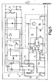
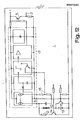
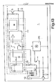
- the exemplary embodiments of electronic switching devices 1 of a circuit arrangement according to the invention shown in FIGS. 5 and 8 to 13 have in common that on the one hand they have an LC resonant circuit 10 which is connected to ground on one side and a trimming and / or hysteresis resistance network 16 which is also connected to ground on the one hand on the other hand, most of the components are monolithically integrated, namely implemented in an integrated circuit 17.
- Different in the exemplary embodiments of electronic switching devices 1 of a circuit arrangement shown in FIGS. 5 and 8 to 13 are the implemented damping and / or damping options of the oscillator 4, in addition to the LC resonant circuit 10 and the balancing and / or Hysteresis resistance network 16 include components realized within the integrated circuit 17. The required damping or damping check pulses are also different.
- check pulse shown are now initially g eneratoren 8 will be described, namely, the g in Fi. 5 in connection with an electronic switching device 1 shown check pulse generator 8 and the in the Fi g. 6 and 7 test pulse generators 8 shown separately.
- each electronic switching device 1 of a circuit arrangement according to the invention can have its own - complete - check pulse generator 8, as shown in FIG. 5.
- the clock pulse processing network 20 of the check pulse generator 8 is designed as a pulse doubler; From the clock pulses of the clock pulse generator 18 arriving at the clock pulse input 21, two successive, equally long checking pulses are available which are available at the checking pulse outputs 22, 23 and from there control the damping switch 14 and the damping switch 15.
- the graphic representation according to FIG. 2 corresponds to the exemplary embodiment shown in FIG. 5.
- the clock pulse processing network 20 of the check pulse generator 8 additionally has a control input 24 which is supplied with a control signal corresponding to the actual output signal of the electronic switching device 1.
- the clock pulse processing network 20 of the check pulse generator 8 must be part of the respective electronic switching device 1.
- the exemplary embodiment shown in FIG. 7 is only slightly modified, namely to the extent that the damping checking pulses - at the checking pulse output 22 of the clock pulse processing network 20 and thus of the checking pulse generator 8 - are continuously available, while the damping checking pulses - At the check pulse output 23 of the clock pulse processing network 20 and thus the check pulse generator 8 - are dependent on the actual output signal of the electronic switching device 1.
- the electronic switching device 1 and the external conductors 6, 7 connected to the electronic switching device 1 may be permissible in a circuit arrangement according to the invention to subject the electronic switching device 1 and the external conductors 6, 7 connected to the electronic switching device 1 to error monitoring only in the “critical switching state”.
- the checking pulse generator 8 therefore only includes the clock pulse generator 18, so a clock pulse processing network 20 is not required.
- the damping of the oscillator 4 takes place in that a damping resistor 12 is connected in parallel in the LC resonant circuit 10, and the damping of the oscillator 4 takes place in that the Trimming and / or hysteresis resistance network 16 Damping resistor 13 is connected in parallel.
- the oscillator 4 of the electronic switching device 1 can also be damped and damped differently.
- the damping of the oscillator 4 of the electronic switching device 1 takes place in that the damping resistor 12 is connected in series to a partial resistance of the balancing and hysteresis resistance network 16, while the damping takes place by the fact that the previously mentioned partial resistance of the balancing resistor and hysteresis resistor network 16, the damping resistor 13 is connected in parallel.
- the check pulse generators 8 shown in FIGS. 5 to 7 can be used for this exemplary embodiment, but the damping check pulses must be inverted.
- the damping of the oscillator 4 of the electronic switching device 1 takes place in that, as in the exemplary embodiments according to FIGS. 5 and 9, the LC resonant circuit 10, the damping resistor 12 is connected in parallel, while the damping takes place in that a damping resistor 13 normally connected in parallel with the LC resonant circuit 10 is "switched off".
- the check pulse generators 8 shown in FIGS. 5 to 7 can again be used for this exemplary embodiment, but this time the damping check pulses must be inverted.
- FIG. 11 The embodiment of an electronic switching device 1 of a circuit arrangement according to the invention shown in FIG. 11 largely corresponds to the embodiment shown in FIG. 10.
- only the parallel damping resistor 13 provided in the exemplary embodiment according to FIG. 11 is replaced by a series-connected damping resistor 13.
- the embodiment of an electronic switching device 1 of a circuit arrangement according to the invention shown in FIG. 13 largely corresponds to the embodiment shown in FIG. 11.
- the damping of the oscillator 4 of the electronic switching device 1 takes place in that high-frequency "damping energy" coming from a high-frequency damping oscillator 25 is fed in.
- an error indicator is part 3.
- Embodiments of such a fault indicator 3 are initially g in Fi. 14 and 1 5 shown.
- the fault indicator 3 consists in its basic structure of an input amplifier 26 (with a trigger stage), which forms and inverts the monitoring pulses arriving at the monitoring pulse input 27 from the output 2 of the electronic switching device 1, from a differentiating stage 28, which is associated with each positive edge of a monitoring pulse coming from the output 2 of the electronic switching device 1 delivers a negative indication pulse, and from an integrating stage 29 with an integrating network 30 and an integrating amplifier 31.
- the integrating stage 29 only delivers a positive control signal to an output transistor 32 if continuously - with an certain repetition frequency - arrive at monitoring pulse input 27 - from output 2 of electronic switching device 1 - monitoring pulses.
- a safety circuit 33 is also provided, which works as an integrating stage with the same time constant for charging and discharging.
- the safety circuit 33 supplies sieved steady positive or negative control signals to the output transistor 32. Consequently, a relay 34 lying in series with the output transistor 32 can only pick up if the monitoring pulse input 27 of the error indicator 3 - coming from the output 2 of the electronic switching device 1 - has one arrives uninterrupted sequence of monitoring pulses, on the other hand, the actual output signal of the electronic switch 1 is positive.
- the exemplary embodiment shown in FIG. 15 of an error indicator 3 belonging to the circuit arrangement according to the invention differs only slightly from the exemplary embodiment shown in FIG. 14, namely in that on the one hand an exclusive OR gate 35 is provided and on the other hand the clock pulse generator which is functionally associated with the checking pulse generator 8 18 is implemented in connection with the error indicator 3.
- the clock pulse output 19 of the clock pulse generator 18 must be connected to the clock pulse input 21 or the clock pulse inputs 21 of the clock pulse processing network 20 implemented within the electronic switching device 1 or of the clock pulse processing networks 20 implemented within the electronic switching devices 1.
- the exclusive OR gate 35 combines the clock pulses and the monitoring pulses ultimately caused by the clock pulses, so that at the output of the exclusive OR gate 35 the actual output signal of the electronic switching device 1 corresponding output signal is present, that is to say an output signal which, unlike the output signal at output 2 of electronic switching device 1, is not superimposed on the monitoring pulses.
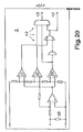
- FIG. 18 to 20 finally show a further exemplary embodiment of a circuit arrangement according to the invention, namely FIG. 18 of the associated electronic switching device 1 and FIG. 20 of the associated fault indicator 3.
- an electronic switching device 1 shown in FIG. 18 initially largely corresponds to the embodiment shown in FIG. 5.
- the check pulse generator 8 shown in FIG. 6 is provided here
- the clock pulse generator 18 belonging to the check pulse generator 8 preferably being operated with a pulse duty factor of 1: 3.
- the electronic switching device 1 also has an analog integrating stage 36 and a voltage / current converter 37.
- At the output of the analog integrating stage 36 there are one third and two thirds of a re fer e n zschreib U ref on.
- the output voltage of the analog integrating stage 36 is converted into a proportional output current of the voltage / current converter 37.
- an output current of the voltage / current converter 37 of 20 mA can be applied for 100 percent of the reference voltage U ref. Then, when the electronic switching device 1 is blocked, an output current of approximately 6.6 mA nominal and then, when the electronic switching device 1 is conductive, an output current of approximately 13.3 mA nominal is obtained. If an error occurs for whatever reason, the output current will tend to 20 mA or 0 mA, which can be evaluated as an error.
- This error indicator 3 initially has a measuring resistor 38 which converts the output current of the voltage / current converter 37 into a proportional measuring voltage.
- This measuring voltage is monitored by comparators 39, 40, 41 set to different thresholds.
- the output signals supplied from the comparators 39, 40, 41 are in a Questionwachungslo g ik 42 linked such that at the monitor output 43 of the logic unit 42 is present only an "actual" output signal when an error is not present.
- the monitoring logic 42 also has an error output 44, at which a positive error signal is present if an error is present.
Landscapes
- Engineering & Computer Science (AREA)
- Physics & Mathematics (AREA)
- General Physics & Mathematics (AREA)
- General Engineering & Computer Science (AREA)
- Computer Security & Cryptography (AREA)
- Electronic Switches (AREA)
- Control Of Indicators Other Than Cathode Ray Tubes (AREA)
- Measurement Of Current Or Voltage (AREA)
Priority Applications (1)
| Application Number | Priority Date | Filing Date | Title |
|---|---|---|---|
| AT83101371T ATE17050T1 (de) | 1982-02-18 | 1983-02-12 | Schaltungsanordnung mit einem schaltgeraet und einem fehlerindikator. |
Applications Claiming Priority (2)
| Application Number | Priority Date | Filing Date | Title |
|---|---|---|---|
| DE3205737 | 1982-02-18 | ||
| DE3205737A DE3205737C2 (de) | 1982-02-18 | 1982-02-18 | Schaltungsanordnung zur Überwachung eines Schaltgerätes und der an ihm angeschlossenen Außenleiter |
Publications (2)
| Publication Number | Publication Date |
|---|---|
| EP0087094A1 true EP0087094A1 (fr) | 1983-08-31 |
| EP0087094B1 EP0087094B1 (fr) | 1985-12-18 |
Family
ID=6156025
Family Applications (1)
| Application Number | Title | Priority Date | Filing Date |
|---|---|---|---|
| EP83101371A Expired EP0087094B1 (fr) | 1982-02-18 | 1983-02-12 | Dispositif électronique comprenant un circuit de commutation et un indicateur de défaut |
Country Status (5)
| Country | Link |
|---|---|
| US (1) | US4525699A (fr) |
| EP (1) | EP0087094B1 (fr) |
| JP (1) | JPS58194428A (fr) |
| AT (1) | ATE17050T1 (fr) |
| DE (2) | DE3205737C2 (fr) |
Cited By (5)
| Publication number | Priority date | Publication date | Assignee | Title |
|---|---|---|---|---|
| EP0075086A3 (fr) * | 1981-09-22 | 1984-10-17 | Robert Buck | Montage avec un appareil commutation et un indicateur d'erreur |
| EP0132850A1 (fr) * | 1983-07-28 | 1985-02-13 | Gebhard Balluff Fabrik feinmechanischer Erzeugnisse GmbH & Co. | Commutateur de proximité auto-contrôlé |
| EP0366960A3 (en) * | 1988-11-04 | 1990-11-28 | Hydac Technology Gmbh | Operation-monitored valve |
| EP0341576A3 (en) * | 1988-05-07 | 1990-12-19 | Gebhard Balluff Fabrik Feinmechanischer Erzeugnisse Gmbh & Co. | Self-checking capacitive proximity switch |
| EP1850140A3 (fr) * | 2006-04-24 | 2011-11-16 | ifm electronic gmbh | Circuit doté d'au moins un capteur et une unité d'évaluation |
Families Citing this family (21)
| Publication number | Priority date | Publication date | Assignee | Title |
|---|---|---|---|---|
| DE3220111C1 (de) * | 1982-05-28 | 1983-06-09 | Honeywell Gmbh, 6050 Offenbach | Überwachungseinrichtung für Näherungsschalter |
| DE3505765A1 (de) * | 1985-02-20 | 1986-08-21 | Werner Turck Gmbh & Co Kg, 5884 Halver | Induktiver naeherungsschalter mit pruefeinrichtung |
| GB2189613B (en) * | 1986-04-24 | 1991-01-09 | Argos Alarms & Security Produc | Monitoring means for testing electrical /electronic circuitry or components |
| GB8704375D0 (en) * | 1987-02-25 | 1987-04-01 | Rentokil Ltd | Pest monitoring system |
| DE3722335A1 (de) * | 1987-07-07 | 1989-01-19 | Ifm Electronic Gmbh | Elektronisches, vorzugsweise beruehrungslos arbeitendes schaltgeraet |
| DE3722334A1 (de) * | 1987-07-07 | 1989-02-09 | Ifm Electronic Gmbh | Elektronisches, beruehrungslos arbeitendes schaltgeraet |
| US4845475A (en) * | 1987-11-17 | 1989-07-04 | The Boeing Company | Automatic testing of position sensing devices employing stored sensed position |
| DE4233922C2 (de) * | 1992-10-08 | 1994-06-23 | Ifm Electronic Gmbh | Induktiver Näherungsschalter |
| DE4238992C2 (de) * | 1992-11-19 | 1996-03-21 | Ifm Electronic Gmbh | Verfahren und Vorrichtung zum berührungslosen Nachweis der Annäherung eines Ansprechkörpers |
| DE19824362A1 (de) * | 1998-05-30 | 1999-12-16 | Micronas Intermetall Gmbh | Verfahren zur Funktionsüberwachung eines Sensorbausteins sowie Sensorbaustein zur Durchführung des Verfahrens |
| EP0969600A1 (fr) * | 1998-07-03 | 2000-01-05 | Siemens Aktiengesellschaft | Commutateur de proximité avec vérification du fonctionnement intégrée |
| AT412636B (de) * | 2000-02-23 | 2005-05-25 | Vae Eisenbahnsysteme Gmbh | Einrichtung zur überwachung und prognose der ausfallwahrscheinlichkeit von induktiven näherungssensoren |
| DE60304049T2 (de) * | 2002-03-29 | 2006-10-26 | Ecolab Inc., Saint Paul | Verfahren und vorrichtung zur automatischen erzeugung von schädlingsfangberichten und zur aufzeichnung zusätzlicher fangparameterdaten |
| US7071829B2 (en) * | 2002-03-29 | 2006-07-04 | Ecolab Inc. | Light extinction based non-destructive flying insect detector |
| DE10329975B4 (de) * | 2003-06-26 | 2005-05-12 | Siemens Ag | Verfahren und Vorrichtung zur Funktionsprüfung eines induktiven Sensors |
| DE102004037683B4 (de) * | 2004-08-02 | 2007-12-06 | Ifm Electronic Gmbh | Sicherheitsschaltung |
| US20090212027A1 (en) * | 2008-02-21 | 2009-08-27 | Hypertherm, Inc. | Binary Signal Detection |
| DE102014222797A1 (de) | 2014-04-17 | 2015-10-22 | Ifm Electronic Gmbh | Elektronisch einstellbarer Rheostat |
| JP7053629B2 (ja) * | 2017-01-06 | 2022-04-12 | バイエル クロップサイエンス エルピー | 無線式動物捕獲器検出システム用センサ |
| US10062254B1 (en) | 2017-04-03 | 2018-08-28 | Alexander Paul | Intrusion detection system |
| JPWO2021014558A1 (ja) * | 2019-07-23 | 2021-09-27 | 三菱電機株式会社 | 入力診断装置及び入力診断方法 |
Citations (5)
| Publication number | Priority date | Publication date | Assignee | Title |
|---|---|---|---|---|
| DE1238811B (de) * | 1959-12-03 | 1967-04-13 | Scully Signal Co | Signaluebertragungsanlage mit Funktionsfaehigkeitsselbstueberwachung |
| DE1951137A1 (de) * | 1969-10-10 | 1971-05-13 | Ifm Gmbh & Co Kg | Induktiver Annaeherungsinitiator |
| DE2626959A1 (de) * | 1976-06-16 | 1977-12-22 | Robert Buck | Pruefgeraet zur ueberpruefung des schwingungszustandes elektronischer, beruehrungslos arbeitender schaltgeraete |
| DE2628427B2 (de) * | 1976-06-24 | 1978-10-26 | Robert 7995 Neukirch Buck | Elektronisches Schaltgerät |
| DE3038141C1 (de) * | 1980-10-09 | 1982-02-18 | Robert 7995 Neukirch Buck | Elektronisches,beruehrungslos arbeitendes Schaltgeraet |
Family Cites Families (7)
| Publication number | Priority date | Publication date | Assignee | Title |
|---|---|---|---|---|
| US3566399A (en) * | 1968-02-27 | 1971-02-23 | Gulf & Western Syst Co | Control station monitoring system for remote stations |
| SE362974B (fr) * | 1973-03-12 | 1973-12-27 | Securitas Ab Bevaknings | |
| FR2324172A1 (fr) * | 1975-09-15 | 1977-04-08 | Gautier Gerard | Dispositif de protection antifrauduleuse pour ligne telephonique exploitee en transmission d'alarme |
| JPS5242472A (en) * | 1975-10-01 | 1977-04-02 | Matsushita Electric Ind Co Ltd | Method of disposing gas purifying composition |
| JPS5265868A (en) * | 1975-11-27 | 1977-05-31 | Matsushita Electric Works Ltd | Proximity switch |
| DE2718459A1 (de) * | 1977-04-26 | 1978-11-02 | Licentia Gmbh | Automatischer naeherungsdetektor fuer raeder schienengebundener fahrzeuge |
| DE3209673C2 (de) * | 1981-09-22 | 1984-07-05 | Robert Ing.(grad.) 7995 Neukirch Buck | Schaltungsanordnung zur Überwachung eines Schaltgerätes und der an ihm angeschlossenen Außenleiter |
-
1982
- 1982-02-18 DE DE3205737A patent/DE3205737C2/de not_active Expired
-
1983
- 1983-02-12 AT AT83101371T patent/ATE17050T1/de not_active IP Right Cessation
- 1983-02-12 DE DE8383101371T patent/DE3361512D1/de not_active Expired
- 1983-02-12 EP EP83101371A patent/EP0087094B1/fr not_active Expired
- 1983-02-16 JP JP58022953A patent/JPS58194428A/ja active Pending
- 1983-02-17 US US06/467,853 patent/US4525699A/en not_active Expired - Fee Related
Patent Citations (5)
| Publication number | Priority date | Publication date | Assignee | Title |
|---|---|---|---|---|
| DE1238811B (de) * | 1959-12-03 | 1967-04-13 | Scully Signal Co | Signaluebertragungsanlage mit Funktionsfaehigkeitsselbstueberwachung |
| DE1951137A1 (de) * | 1969-10-10 | 1971-05-13 | Ifm Gmbh & Co Kg | Induktiver Annaeherungsinitiator |
| DE2626959A1 (de) * | 1976-06-16 | 1977-12-22 | Robert Buck | Pruefgeraet zur ueberpruefung des schwingungszustandes elektronischer, beruehrungslos arbeitender schaltgeraete |
| DE2628427B2 (de) * | 1976-06-24 | 1978-10-26 | Robert 7995 Neukirch Buck | Elektronisches Schaltgerät |
| DE3038141C1 (de) * | 1980-10-09 | 1982-02-18 | Robert 7995 Neukirch Buck | Elektronisches,beruehrungslos arbeitendes Schaltgeraet |
Cited By (6)
| Publication number | Priority date | Publication date | Assignee | Title |
|---|---|---|---|---|
| EP0075086A3 (fr) * | 1981-09-22 | 1984-10-17 | Robert Buck | Montage avec un appareil commutation et un indicateur d'erreur |
| EP0132850A1 (fr) * | 1983-07-28 | 1985-02-13 | Gebhard Balluff Fabrik feinmechanischer Erzeugnisse GmbH & Co. | Commutateur de proximité auto-contrôlé |
| WO1985000712A1 (fr) * | 1983-07-28 | 1985-02-14 | Gebhard Balluff Fabrik Feinmechanischer Erzeugniss | Commutateur capacitif a controle automatique |
| EP0341576A3 (en) * | 1988-05-07 | 1990-12-19 | Gebhard Balluff Fabrik Feinmechanischer Erzeugnisse Gmbh & Co. | Self-checking capacitive proximity switch |
| EP0366960A3 (en) * | 1988-11-04 | 1990-11-28 | Hydac Technology Gmbh | Operation-monitored valve |
| EP1850140A3 (fr) * | 2006-04-24 | 2011-11-16 | ifm electronic gmbh | Circuit doté d'au moins un capteur et une unité d'évaluation |
Also Published As
| Publication number | Publication date |
|---|---|
| JPS58194428A (ja) | 1983-11-12 |
| EP0087094B1 (fr) | 1985-12-18 |
| DE3361512D1 (en) | 1986-01-30 |
| DE3205737C2 (de) | 1984-07-05 |
| ATE17050T1 (de) | 1986-01-15 |
| DE3205737A1 (de) | 1983-09-01 |
| US4525699A (en) | 1985-06-25 |
Similar Documents
| Publication | Publication Date | Title |
|---|---|---|
| EP0087094B1 (fr) | Dispositif électronique comprenant un circuit de commutation et un indicateur de défaut | |
| EP0169468B1 (fr) | Appareil de commutation électronique, de préférence à fonctionnement sans contact | |
| DE3209673C2 (de) | Schaltungsanordnung zur Überwachung eines Schaltgerätes und der an ihm angeschlossenen Außenleiter | |
| EP0092711B2 (fr) | Appareil de commutation électronique, de préférence sans contact actionné | |
| DE3320975C2 (de) | Elektronisches, vorzugsweise berührungslos arbeitendes Schaltgerät | |
| DE3722335C2 (fr) | ||
| DE3722334C2 (fr) | ||
| DE3420236A1 (de) | Elektronisches, vorzugsweise beruehrungslos arbeitendes schaltgeraet | |
| DE4023502C2 (fr) | ||
| EP0468424B1 (fr) | Appareil de commutation électronique avec indicateur de présence | |
| DE3605499C1 (en) | Electronic switching device preferably operating contactlessly | |
| DE3327328A1 (de) | Elektronisches, beruehrungslos arbeitendes schaltgeraet | |
| DE3723008C1 (en) | Electronic switching device preferably operating contactlessly | |
| EP0164511B1 (fr) | Circuit de contrôle pour détecter le dépassement des valeurs limites données | |
| DE4023529C2 (fr) | ||
| EP0298329B1 (fr) | Appareil de commutation électronique fonctionnant de préférence sans contact | |
| DE4111297C1 (fr) | ||
| EP0461550B1 (fr) | Appareil de commutation électronique avec indicateur d'état | |
| EP0743750A1 (fr) | Dispositif électronique de commutation, de préférence avec opération sans contact | |
| EP0299259B1 (fr) | Appareil de commutation électronique, fonctionnant de préférence sans contact | |
| DE3744756A1 (de) | Konstantstromgenerator | |
| DE1275419B (de) | Anordnung zum kontaktlosen Schalten von Signallampen |
Legal Events
| Date | Code | Title | Description |
|---|---|---|---|
| PUAI | Public reference made under article 153(3) epc to a published international application that has entered the european phase |
Free format text: ORIGINAL CODE: 0009012 |
|
| AK | Designated contracting states |
Designated state(s): AT BE CH DE FR GB IT LI LU NL SE |
|
| 17P | Request for examination filed |
Effective date: 19840208 |
|
| GRAA | (expected) grant |
Free format text: ORIGINAL CODE: 0009210 |
|
| AK | Designated contracting states |
Designated state(s): AT BE CH DE FR GB IT LI LU NL SE |
|
| REF | Corresponds to: |
Ref document number: 17050 Country of ref document: AT Date of ref document: 19860115 Kind code of ref document: T |
|
| ITF | It: translation for a ep patent filed | ||
| REF | Corresponds to: |
Ref document number: 3361512 Country of ref document: DE Date of ref document: 19860130 |
|
| ET | Fr: translation filed | ||
| PGFP | Annual fee paid to national office [announced via postgrant information from national office to epo] |
Ref country code: AT Payment date: 19860207 Year of fee payment: 4 |
|
| PG25 | Lapsed in a contracting state [announced via postgrant information from national office to epo] |
Ref country code: LU Free format text: LAPSE BECAUSE OF NON-PAYMENT OF DUE FEES Effective date: 19860228 |
|
| PGFP | Annual fee paid to national office [announced via postgrant information from national office to epo] |
Ref country code: NL Payment date: 19860228 Year of fee payment: 4 |
|
| PGFP | Annual fee paid to national office [announced via postgrant information from national office to epo] |
Ref country code: LU Payment date: 19860404 Year of fee payment: 4 |
|
| PLBI | Opposition filed |
Free format text: ORIGINAL CODE: 0009260 |
|
| 26 | Opposition filed |
Opponent name: PULSOTRONIC MERTEN GMBH & CO. KG Effective date: 19860906 |
|
| NLR1 | Nl: opposition has been filed with the epo |
Opponent name: PULSOTRONIC MERTEN GMBH & CO. KG |
|
| PG25 | Lapsed in a contracting state [announced via postgrant information from national office to epo] |
Ref country code: AT Effective date: 19870212 |
|
| PG25 | Lapsed in a contracting state [announced via postgrant information from national office to epo] |
Ref country code: SE Effective date: 19870213 |
|
| PG25 | Lapsed in a contracting state [announced via postgrant information from national office to epo] |
Ref country code: LI Effective date: 19870228 Ref country code: CH Effective date: 19870228 |
|
| PLBM | Termination of opposition procedure: date of legal effect published |
Free format text: ORIGINAL CODE: 0009276 |
|
| STAA | Information on the status of an ep patent application or granted ep patent |
Free format text: STATUS: OPPOSITION PROCEDURE CLOSED |
|
| 27C | Opposition proceedings terminated |
Effective date: 19870224 |
|
| BERE | Be: lapsed |
Owner name: I F M ELECTRONIC G.M.B.H. Effective date: 19870228 |
|
| PG25 | Lapsed in a contracting state [announced via postgrant information from national office to epo] |
Ref country code: NL Effective date: 19870901 |
|
| GBPC | Gb: european patent ceased through non-payment of renewal fee | ||
| NLV4 | Nl: lapsed or anulled due to non-payment of the annual fee | ||
| PG25 | Lapsed in a contracting state [announced via postgrant information from national office to epo] |
Ref country code: FR Free format text: LAPSE BECAUSE OF NON-PAYMENT OF DUE FEES Effective date: 19871030 |
|
| REG | Reference to a national code |
Ref country code: CH Ref legal event code: PL |
|
| REG | Reference to a national code |
Ref country code: FR Ref legal event code: ST |
|
| PG25 | Lapsed in a contracting state [announced via postgrant information from national office to epo] |
Ref country code: GB Effective date: 19881122 |
|
| PG25 | Lapsed in a contracting state [announced via postgrant information from national office to epo] |
Ref country code: BE Effective date: 19890228 |
|
| EUG | Se: european patent has lapsed |
Ref document number: 83101371.9 Effective date: 19880215 |
|
| PGFP | Annual fee paid to national office [announced via postgrant information from national office to epo] |
Ref country code: DE Payment date: 19990305 Year of fee payment: 17 |
|
| PG25 | Lapsed in a contracting state [announced via postgrant information from national office to epo] |
Ref country code: DE Free format text: LAPSE BECAUSE OF NON-PAYMENT OF DUE FEES Effective date: 20001201 |
|
| PLAB | Opposition data, opponent's data or that of the opponent's representative modified |
Free format text: ORIGINAL CODE: 0009299OPPO |
|
| PLAB | Opposition data, opponent's data or that of the opponent's representative modified |
Free format text: ORIGINAL CODE: 0009299OPPO |
|
| R26 | Opposition filed (corrected) |
Opponent name: PULSOTRONIC MERTEN GMBH & CO. KG Effective date: 19860906 |