EP0087590A2 - Elektrochemische Zelle mit festen Elektroden und einem zwischenliegenden ionenleitenden keramischen Festelektrolyten - Google Patents
Elektrochemische Zelle mit festen Elektroden und einem zwischenliegenden ionenleitenden keramischen Festelektrolyten Download PDFInfo
- Publication number
- EP0087590A2 EP0087590A2 EP83100792A EP83100792A EP0087590A2 EP 0087590 A2 EP0087590 A2 EP 0087590A2 EP 83100792 A EP83100792 A EP 83100792A EP 83100792 A EP83100792 A EP 83100792A EP 0087590 A2 EP0087590 A2 EP 0087590A2
- Authority
- EP
- European Patent Office
- Prior art keywords
- solid electrolyte
- electrode
- ceramic substrate
- electronic
- layer
- Prior art date
- Legal status (The legal status is an assumption and is not a legal conclusion. Google has not performed a legal analysis and makes no representation as to the accuracy of the status listed.)
- Granted
Links
Images

Classifications
-
- G—PHYSICS
- G02—OPTICS
- G02F—OPTICAL DEVICES OR ARRANGEMENTS FOR THE CONTROL OF LIGHT BY MODIFICATION OF THE OPTICAL PROPERTIES OF THE MEDIA OF THE ELEMENTS INVOLVED THEREIN; NON-LINEAR OPTICS; FREQUENCY-CHANGING OF LIGHT; OPTICAL LOGIC ELEMENTS; OPTICAL ANALOGUE/DIGITAL CONVERTERS
- G02F1/00—Devices or arrangements for the control of the intensity, colour, phase, polarisation or direction of light arriving from an independent light source, e.g. switching, gating or modulating; Non-linear optics
- G02F1/01—Devices or arrangements for the control of the intensity, colour, phase, polarisation or direction of light arriving from an independent light source, e.g. switching, gating or modulating; Non-linear optics for the control of the intensity, phase, polarisation or colour
- G02F1/15—Devices or arrangements for the control of the intensity, colour, phase, polarisation or direction of light arriving from an independent light source, e.g. switching, gating or modulating; Non-linear optics for the control of the intensity, phase, polarisation or colour based on an electrochromic effect
- G02F1/153—Constructional details
-
- G—PHYSICS
- G02—OPTICS
- G02F—OPTICAL DEVICES OR ARRANGEMENTS FOR THE CONTROL OF LIGHT BY MODIFICATION OF THE OPTICAL PROPERTIES OF THE MEDIA OF THE ELEMENTS INVOLVED THEREIN; NON-LINEAR OPTICS; FREQUENCY-CHANGING OF LIGHT; OPTICAL LOGIC ELEMENTS; OPTICAL ANALOGUE/DIGITAL CONVERTERS
- G02F1/00—Devices or arrangements for the control of the intensity, colour, phase, polarisation or direction of light arriving from an independent light source, e.g. switching, gating or modulating; Non-linear optics
- G02F1/01—Devices or arrangements for the control of the intensity, colour, phase, polarisation or direction of light arriving from an independent light source, e.g. switching, gating or modulating; Non-linear optics for the control of the intensity, phase, polarisation or colour
- G02F1/15—Devices or arrangements for the control of the intensity, colour, phase, polarisation or direction of light arriving from an independent light source, e.g. switching, gating or modulating; Non-linear optics for the control of the intensity, phase, polarisation or colour based on an electrochromic effect
- G02F1/1514—Devices or arrangements for the control of the intensity, colour, phase, polarisation or direction of light arriving from an independent light source, e.g. switching, gating or modulating; Non-linear optics for the control of the intensity, phase, polarisation or colour based on an electrochromic effect characterised by the electrochromic material, e.g. by the electrodeposited material
- G02F1/1523—Devices or arrangements for the control of the intensity, colour, phase, polarisation or direction of light arriving from an independent light source, e.g. switching, gating or modulating; Non-linear optics for the control of the intensity, phase, polarisation or colour based on an electrochromic effect characterised by the electrochromic material, e.g. by the electrodeposited material comprising inorganic material
- G02F1/1525—Devices or arrangements for the control of the intensity, colour, phase, polarisation or direction of light arriving from an independent light source, e.g. switching, gating or modulating; Non-linear optics for the control of the intensity, phase, polarisation or colour based on an electrochromic effect characterised by the electrochromic material, e.g. by the electrodeposited material comprising inorganic material characterised by a particular ion transporting layer, e.g. electrolyte
-
- H—ELECTRICITY
- H01—ELECTRIC ELEMENTS
- H01M—PROCESSES OR MEANS, e.g. BATTERIES, FOR THE DIRECT CONVERSION OF CHEMICAL ENERGY INTO ELECTRICAL ENERGY
- H01M6/00—Primary cells; Manufacture thereof
- H01M6/14—Cells with non-aqueous electrolyte
- H01M6/18—Cells with non-aqueous electrolyte with solid electrolyte
-
- H—ELECTRICITY
- H05—ELECTRIC TECHNIQUES NOT OTHERWISE PROVIDED FOR
- H05K—PRINTED CIRCUITS; CASINGS OR CONSTRUCTIONAL DETAILS OF ELECTRIC APPARATUS; MANUFACTURE OF ASSEMBLAGES OF ELECTRICAL COMPONENTS
- H05K1/00—Printed circuits
- H05K1/02—Details
- H05K1/03—Use of materials for the substrate
- H05K1/0306—Inorganic insulating substrates, e.g. ceramic, glass
-
- Y—GENERAL TAGGING OF NEW TECHNOLOGICAL DEVELOPMENTS; GENERAL TAGGING OF CROSS-SECTIONAL TECHNOLOGIES SPANNING OVER SEVERAL SECTIONS OF THE IPC; TECHNICAL SUBJECTS COVERED BY FORMER USPC CROSS-REFERENCE ART COLLECTIONS [XRACs] AND DIGESTS
- Y02—TECHNOLOGIES OR APPLICATIONS FOR MITIGATION OR ADAPTATION AGAINST CLIMATE CHANGE
- Y02P—CLIMATE CHANGE MITIGATION TECHNOLOGIES IN THE PRODUCTION OR PROCESSING OF GOODS
- Y02P70/00—Climate change mitigation technologies in the production process for final industrial or consumer products
- Y02P70/50—Manufacturing or production processes characterised by the final manufactured product
Definitions
- the invention relates to a ceramic substrate as a carrier for electronic components and integrated electronic circuits.
- a problem with large-scale integration is, in particular, the uncontrolled thermal load resulting from the accumulation of electrical components, since the thermal conductivity of plastics is too low. to ensure controlled thermal dissipation. In addition, the softening point of the plastic circuit boards is so low that the electrical switching architecture is disturbed.
- the invention is therefore based on the object of making available a ceramic substrate for the application of both electronic, optical and electrochemical components, which permits an integral coupling and functioning of these elements.
- the first-mentioned mixed crystal series which should be preferred for reasons of particularly good ion conductivity at room temperature, is described in more detail in the older German patent application P 30 32 894, the second mixed crystal series in the older German patent application P 31 23 099.
- solid-state electrolytes according to the invention as a carrier material are of several types: because of the very low electron conductivity, they are practically electrical insulators and thus can be used as substrate holders for the electronic components such as microprocessors and / or quartz drivers. They are even preferable to the previously used ⁇ -corundum for this task, since the material according to the invention has a lower sintering temperature of about 1250 ° C, compared to 1650 to 1750 ° C with ⁇ -corundum, is available and on the other hand has a higher resistance to temperature changes.
- the second function of the ceramic substrate according to the invention is that because of its ionic conductivity it can directly take on the role of the electrolyte for solid-state batteries based on Na, while on the other hand it fulfills the condition of a carrier for layer circuits due to its electronic insulation properties mentioned above.
- this offers the integration of electronic and electrochemical components on a common carrier substrate.
- suitable coating technologies such as vapor deposition, screen printing, etc., it is possible to produce individual substrates from the plasticized film continuously, inexpensively.
- a battery e.g. for storage maintenance or as an electrical power supply
- the plasticized ceramic substrate is either suitably preformed at the location provided for the power source, e.g. by applying raised structures, or by adding burn-out substances such as starch compounds to a particular one porous formation of the ceramic substrate takes place.
- the active materials such as sodium for the anode side and compounds such as AlCl 3 , BiCJ 3 or WCl 6 for the cathode side can be applied to these structured areas in the molten state. For materials with melting points above 200 ° C or with high vapor pressures, it is advisable to press these materials onto the substrate holder.
- the ceramic substrate according to the invention advantageously opens up the possibility here of using a multilayer structure not only to distribute the electronic conductor tracks over several levels, but also to provide cavities which can be filled with the active material in a molten state after the substrate has been fired. After the active masses have solidified, the feed holes can be closed, for example with a glass solder, and the power sources are therefore integrated in the multilayer structure.
- the metallic arresters are applied to the structure before the firing process.
- the ceramic substrate also serves as a solid electrolyte for an electrochromic display (ECD), thus completing the integrability of electronic components with optical and electrochemical components on a ceramic multilayer housing.
- ECD electrochromic display
- the white color of the solid-state electrolyte according to the invention proves to be very favorable if a solid-state ECD with e.g. WO-, which contrasts against blue background due to electrochemical processes (diffusion of Na ions) against a white background.
- the power supply for the ECD can be separated e.g. be installed in the same multilayer housing under the ECD; this would mean a low overall height for an area that is only determined by the display screen.
- this display also has the favorable property of storing the information.
- Figure 1 shows an example of a preferred embodiment of the invention.
- the multilayer housing 1 which can be produced according to modern methods of ceramic technology, from a sodium zirconium phosphatosilicate solid electrolyte according to the invention contains a positive battery electrode 2 and a negative Na electrode 3, furthermore a sodium tungsten electrode 4 and on the top layer as their Counterelectrode is a W0 3 coating 5 which is evaporated in segments and only partially covers the white layer surface.
- the latter electrodes together with a Si0 2 insulator layer 6 and a transparent conductor 7 made of Sn-doped In 2 O 3 and the cover glass 8 form a complete electrochromic Display.
- Conductor tracks made of Au, Pt or other noble metals connect all of these electrochemical components to control electronics 10 arranged in the foot of the housing, which here consists, for example, of a microprocessor 11 and a quartz driver stage 12, both encapsulated.
- the two positive electrode functions 2 and 4 on only one positive electrode, e.g. the sodium tungstate electrode 4, to combine, so that the energy supply of the electronic components and the ECD takes place from a common electrochemical power source. In this way, one of the pockets for receiving active positive electrode material can be saved.
- the invention thus makes it possible for the first time to combine electronic, optical and electrochemical functions on one and the same ceramic substrate holder.
- the processor logic is programmable, this concept enables a multitude of device functions such as time clock, multimeter function, etc. to be implemented with one design.
- the possibility of technically handling plasticized ceramic tapes shows the way to cost-effective production.
Landscapes
- Physics & Mathematics (AREA)
- Nonlinear Science (AREA)
- Chemical & Material Sciences (AREA)
- Optics & Photonics (AREA)
- Chemical Kinetics & Catalysis (AREA)
- Electrochemistry (AREA)
- General Physics & Mathematics (AREA)
- Engineering & Computer Science (AREA)
- Inorganic Chemistry (AREA)
- Manufacturing & Machinery (AREA)
- General Chemical & Material Sciences (AREA)
- Compositions Of Oxide Ceramics (AREA)
- Secondary Cells (AREA)
- Electrochromic Elements, Electrophoresis, Or Variable Reflection Or Absorption Elements (AREA)
- Semiconductor Integrated Circuits (AREA)
- Structure Of Printed Boards (AREA)
- Electric Double-Layer Capacitors Or The Like (AREA)
- Conductive Materials (AREA)
- Primary Cells (AREA)
Abstract
Description
- Die Erfindung betrifft ein Keramiksubstrat als Träger für elektronische Bauelemente und integrierte elektronische Schaltkreise.
- Die Entwicklung elektronischer Bauelemente tendiert dahin, daß durch Großintegration immer mehr elektronische Funktionen auf immer weniger Raum konzentriert werden. Diese Entwicklung umfaßt sowohl passive Bauelemente wie z.B. Speicherelemente als auch aktive Elemente wie z.B. Optokoppler. Die Verbindung der einzelnen elektronischen Bauelemente zu Schaltungen geschieht nach dem Stand der Technik auf sog. Leiterplatinen, das sind Kunststoffplatten mit aufgedruckten, eingeätzten oder photochemisch erzeugten Leitungsbahnen der Schaltkreise. Der Integrationsgrad auf diesen Platinen ist ebenfalls als Folge der Entwicklung zunehmend gestiegen, stößt aber materialbedingt durch die Zusammensetzung des Trägermaterials an eine Grenze, die durch die Leitfähigkeit, die thermische Belastbarkeit und die chemische Stabilität des Materials gegeben ist.
- Ein Problem bei der Großintegration ist insbesondere die durch die Anhäufung elektrischer Bauteile entstehende unkontrollierte Wärmebelastung, da die thermische Leitfähigkeit von Kunststoffen zu gering ist. um eine kontrollierte thermische Ableitung zu gewährleisten. Außerdem ist der Erweichungspunkt der Kunststoffplatinen so niedrig, daß die elektrische Schaltarchitektur gestört wird.
- Aus der DE-OS 27 27 364 ist ein Verfahren zur Herstellung eines bandförmigen Keramiksubstrats auf der Basis von Tonerde durch Strangpressen und Glühen der geschnittenen Formstücke bekannt, die sich als keramische Platinen von hoher thermischer Belastbarkeit anbieten. Die ungebrannten Grünlinge sind einer Plastifizierung zugänglich, so daß Platinen beliebiger Struktur und Größe gewalzt und gebrannt werden können. Die Oberflächengüte der erhaltenen Substrate erlaubt die Aufbringung von Leiterbahnen sowohl für Dickschicht- als auch für Dünnschichtschaltungen. Gemäß der Europäischen Patentanmeldung 0036 435 A 1 ist es sogar mit geeigneten Techniken möglich, keramische Mehrschichtgehäuse zur Aufnahme elektronischer Schaltungen herzustellen, die einen noch höheren Integrationsgrad erlauben.
- Parallel mit den Fortschritten der Mikroelektronik vollzog sich, jeweils gesondert für sich, die Miniaturisierung der zum Betreiben der Elektronik notwendigen Batterien in Form der Knopfzellen und die Fortentwicklung der in elektronischen Geräten vorhandenen Anzeigen, die entweder auf stromintensive, aber kontraststarke LED-Systeme oder auf sehr kontrastarme, dafür hochohmige LCD-Systeme zurückgehen.
- Der Erfindung liegt daher die Aufgabe zugrunde, ein keramisches Substrat für die Aufbringung sowohl elektronischer, optischer als auch elektrochemischer Bauelemente verfügbar zu machen, welches eine integrale Verkoppelung und Funktionsweise dieser Elemente gestattet.
- Die Aufgabe wird erfindungsgemäß dadurch gelöst, daß das Substrat ein ionenleitender Festkörperelektrolyt mit einer Mindestleitfähigkeit ∈ = 10-3Ω-1 cm-1 bei Raumtemperatur ist.
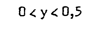
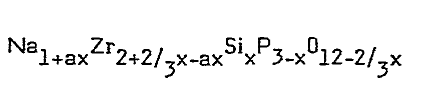
- Ein besonders vorteilhaftes Festkörperelektrolytmaterial besteht aus Mischkristallen der allgemeinen Zusammensetzung Na1+xZr2-1/3x+ySixP3-xO12-2/3x+2y mit den Laufparametern 0,01<x< 3 und 0 < y < 0,5 oder Na1+axZr2+2/3x-axSixP3-xO12-2/3xmits=konst. Zahlenwert zwischen 0,8 und 0,9 und dem Laufparamter 1,8 < x< 2,3.
- Die erstgenannte Mischkristallreihe, welcher aus Gründen einer besonders guten Ionenleitfähigkeit bei Raumtemperatur der Vorzug zu geben ist, ist in der älteren deutschen Patentanmeldung P 30 32 894, die zweite Mischkristallreihe in der älteren deutschen Patentanmeldung P 31 23 099 näher beschrieben.
- Die Gründe für die besondere Eignung erfindungsgemäßer Festkörperelektrolyte als Trägermaterial sind mehrfacher Art: wegen der sehr geringen Elektronenleitfähigkeit sind sie praktisch elektrische Isolatoren und damit als Substrathalter für die elektronischen Komponenten wie Mikroprozessoren und/oder Quarztreiber verwendbar. Sie sind für diese Aufgabe dem bisher eingesetzten α-Korund sogar vorzuziehen, da das erfindungsgemäße Material bei einer niedrigeren Sintertemperatur von etwa 1250°C, im Vergleich zu 1650 bis 1750°C bei α-Korund,erhaltlich ist und andererseits eine höhere Temperaturwechselbeständigkeit besitzt. Den Beweis dafür lieferte ein Vergleich zwischen einem Material aus der vorgenannten deutschen Patentanmeldung P 30 32 894 mit der vorzugsweisen Zusammensetzung Na2,94Zr1,40Si2,2P0,8O10,53 und α -Korund nach DIN 51068. Bei vergleichbaren äußeren Abmessungen der Probekörper war die erfindungsgemäße Zusammensetzung erst nach 6 Aufheiz-und Abkühlzyklen in verschiedene Teile gesprungen, während α -Korund aufgrund seiner geringen Temperaturwechselbeständigkeit schon nach dem ersten Zyklus gesprungen ist.
- Die zweite Funktion des erfindungsgemäßen Keramiksubstrats besteht darin, daß es wegen seiner Ionenleitfähigkeit unmittelbar die Rolle des Elektrolyten für Festkörperbatterien auf Na-Basis übernehmen kann, während es andererseits aufgrund seiner ober erwähnten elektronischen Isolationseigenschaften die Bedingung eines Trägers für Schichtschaltungen erfüllt. Damit aber bietet sich die Integration von elektronischen und elektrochemischen Bauelemente auf einem gemeinsamen Trägersubstrat an. Zugleich wird unter Einbeziehung geeigneter Beschichtungstechnologien wie Aufdampfen, Siebdrucken usw. eine kontinuierliche, kostengünstige Fertigung von Einzelsubstraten aus der plastifizierten Folie möglich.
- Eine Batterie, z.B. für die Speichererhaltung oder als elektrische Stromversorgung, kann derart integriert werden, daß an der für die Stromquelle vorgesehenen Stelle das plastifizierte Keramiksubstrat entweder geeignet vorgeformt wird, z.B. durch Aufbringen erhabener Strukturen, oder daß durch Zugabe von Ausbrennstoffen wie z.B. Stärkeverbindungen eine besonders poröse Ausbildung des Keramiksubstrates erfolgt. Die aktiven Materialien wie z.B. Natrium für die Anodenseite und Verbindungen wie z.B. AlCl3, BiCJ3 oder WCl6 für die Kathodenseite können im schmelzflüssigen Zustand auf diese strukturierten Stellen aufgebracht werden. Bei Materialien mit Schmelzpunkten oberhalb 200°C oder mit hohen Dampfdrücken empfiehlt es sich, diese Materialien auf den Substrathalter aufzupressen. Da Na-basierende elektrochemische Elemente wegen der hohen Reaktivität von Natrium bzw. seiner Verbindungen mit Wasser bzw. Sauerstoff unter Schutzgas abgeschlossen betrieben werden müssen, müssen Anoden- bzw. Kathodenbauteile auf dem Substrathalter geeignet eingekapselt werden. Das erfindungsgemäße Keramiksubstrat eröffnet hier in vorteilhafter Weise die Möglichkeit, durch eine Mehrschichtstruktur nicht nur die elektronischen Leiterbahnen über mehrere Ebenen zu verteilen, sondern auch Hohlräume vorzusehen, die nach dem Brennen des Substrats mit dem aktiven Material schmelzflüssig gefüllt werden können. Nachdem die aktiven Massen erstarrt sind, können die Zuführungslöcher z.B. mit einem Glaslot verschlossen werden, die Stromquellen sind mithin in der Vielschichtstruktur integriert. Die metallischen Ableiter werden bereits vor dem Brennprozeß auf die Struktur aufgebracht.
- In einer besonders vorteilhaften Ausführungsform der Erfindung dient das Keramiksubstrat auch noch als Festelektrolyt für eine elektrochrome Anzeige (ECD), vervollständigt somit die Integrierbarkeit elektronischer Bauelemente mit optischen und elektrochemischen Bauteilen auf einem keramischen Mehrschichtgehäuse. Hierbei erweist sich die weiße Farbe des erfindungsgemäßen Festkörperelektrolyten als sehr günstig, wenn man ein Festkörper-ECD mit z.B. WO-, verwendet, welches durch Blaufärbung infolge elektrochemischer Vorgänge (Diffusion von Na -Ionen) vor einem weißen Hintergrund kontrastreich absticht. Die Stromversorgung für das ECD kann getrennt z.B. im gleichen Mehrschichtgehäuse unter dem ECD angebracht werden; dies würde eine geringe Bauhöhe bei einer Fläche bedeuten, die nur durch den Anzeigeschirm bestimmt ist. Diese Anzeige hat neben der Augenfälligkeit auch die günstige Eigenschaft der Speicherbarkeit der Information.
- Figur 1 zeigt ein Beispiel einer vorzugsweisen Ausführungsform der Erfindung.
- Das nach modernen Methoden der Keramiktechnologie herstellbare Mehrschichtgehäuse 1 aus einem erfindungsgemäßen Natriumzirkonphosphatosilikat-Festkörperelektrolyten enthält in den durch die Schichten gebildeten Zwischenräumen, der Reihe nach von unten, eine positive Batterieelektrode 2 und eine negative Na-Elektrode 3, des weiteren eine Natriumwolframat-Elektrode 4 und auf der obersten Schicht als deren Gegenelektrode eine in Segmenten aufgedampfte und die weiße Schichtoberfläche nur zum Teil bedeckende W03-Belegung 5. Letztere Elektroden bilden zusammen mit einer Si02-Isolatorschicht 6 und einem transparenten Ableiter 7 aus Sn-dotiertem In2O3 sowie dem Deckglas 8 ein vollständiges elektrochromes Display. Leiterbahnen aus Au, Pt oder anderen Edelmetallen verbinden alle diese elektrochemischen Bauelemente mit einer im Fuß des Gehäuses angeordneten Ansteuerelektronik 10, die hier z.B. aus einem Mikroprozessor 11 und einer Quarztreiberstufe 12, beide verkapselt, besteht.
- Es ist sogar möglich, die beiden positiven Elektrodenfunktionen 2 und 4 auf nur eine positive Elektrode, z.B. die Natriumwolframat-Elektrode 4, zu vereinigen, so daß die Energieversorgung der elektronischen Bauelemente und des ECD aus einer gemeinsamen elektrochemischen Stromquelle heraus erfolgt. Auf diese Weise kann eine der Taschen zur Aufnahme von aktivem positiven Elektrodenmaterial eingespart werden.
- Die Erfindung gestattet es somit erstmals, elektronische, optische und elektrochemische Funktionen auf ein und demselben keramischen Substrathalter zu vereinigen. Eine programmierbare Prozessorlogik vorausgesetzt, ermöglicht dieses Konzept eine Vielzahl von Gerätefunktionen wie Zeituhr, Multimeterfunktion usw. mit einem Aufbau zu erfüllen. Die Möglichkeit, plastifizierte Keramikbänder technisch zu handhaben, zeigt den Weg zu einer kostengünstigen Fertigung.
Claims (6)


Priority Applications (1)
| Application Number | Priority Date | Filing Date | Title |
|---|---|---|---|
| AT83100792T ATE51321T1 (de) | 1982-02-27 | 1983-01-28 | Elektrochemische zelle mit festen elektroden und einem zwischenliegenden ionenleitenden keramischen festelektrolyten. |
Applications Claiming Priority (2)
| Application Number | Priority Date | Filing Date | Title |
|---|---|---|---|
| DE19823207131 DE3207131A1 (de) | 1982-02-27 | 1982-02-27 | Keramiksubstrat als traeger fuer elektronische bauelemente und integrierte elektronische schaltkreise |
| DE3207131 | 1983-02-27 |
Publications (3)
| Publication Number | Publication Date |
|---|---|
| EP0087590A2 true EP0087590A2 (de) | 1983-09-07 |
| EP0087590A3 EP0087590A3 (en) | 1985-12-04 |
| EP0087590B1 EP0087590B1 (de) | 1990-03-21 |
Family
ID=6156889
Family Applications (1)
| Application Number | Title | Priority Date | Filing Date |
|---|---|---|---|
| EP83100792A Expired - Lifetime EP0087590B1 (de) | 1982-02-27 | 1983-01-28 | Elektrochemische Zelle mit festen Elektroden und einem zwischenliegenden ionenleitenden keramischen Festelektrolyten |
Country Status (5)
| Country | Link |
|---|---|
| US (1) | US4504120A (de) |
| EP (1) | EP0087590B1 (de) |
| JP (1) | JPS58204405A (de) |
| AT (1) | ATE51321T1 (de) |
| DE (2) | DE3207131A1 (de) |
Cited By (3)
| Publication number | Priority date | Publication date | Assignee | Title |
|---|---|---|---|---|
| EP1862849A1 (de) * | 2006-05-30 | 2007-12-05 | Schefenacker Vision Systems France | Elektrochrome Zelle, ihre Verwendung in Fensterscheiben und Rückspielgel, und ihre Herstellungsmethode |
| CN103512832A (zh) * | 2013-10-09 | 2014-01-15 | 广东生益科技股份有限公司 | 检测压板胶水流动状态的方法 |
| CN107635937A (zh) * | 2015-03-12 | 2018-01-26 | 弗劳恩霍夫应用研究促进协会 | 用于电化学电池中的钠离子传导元件及其制造方法 |
Families Citing this family (6)
| Publication number | Priority date | Publication date | Assignee | Title |
|---|---|---|---|---|
| USRE34469E (en) * | 1987-06-18 | 1993-12-07 | Eic Laboratories, Inc. | Solid state electrochromic light modulator |
| US4938571A (en) * | 1987-06-18 | 1990-07-03 | Cogan Stuart F | Solid state electrochromic light modulator |
| US5336273A (en) * | 1992-11-27 | 1994-08-09 | Gould Electronics Inc. | Laser sealed solid electrolyte cell housed within a ceramic frame and the method for producing it |
| US5314507A (en) * | 1992-11-27 | 1994-05-24 | Gould Electronics Inc. | Adhesive sealed solid electrolyte cell housed within a ceramic frame and the method for producing it |
| FR2748605B1 (fr) * | 1996-05-07 | 1998-08-07 | Gerard Lemaire | Procede de fabrication d'un generateur elementaire de pile ou d'accumulateur intelligent |
| DE102006025070A1 (de) * | 2006-05-23 | 2007-11-29 | Schefenacker Vision Systems Germany Gmbh | Außenspiegel eines Fahrzeugs |
Family Cites Families (8)
| Publication number | Priority date | Publication date | Assignee | Title |
|---|---|---|---|---|
| FR2282171A1 (fr) * | 1974-08-14 | 1976-03-12 | Comp Generale Electricite | Nouvelle structure de generateur electrochimique a electrolyte solide |
| US4105807A (en) * | 1975-07-28 | 1978-08-08 | Unican Electrochemical Products Ltd. | Production of thin, stable, solid electrolyte films of high ionic conductivity |
| US4106862A (en) * | 1976-11-12 | 1978-08-15 | Texas Instruments Incorporated | Electrochromic display cell |
| DE3016524A1 (de) * | 1980-04-29 | 1981-11-05 | Max-Planck-Gesellschaft zur Förderung der Wissenschaften e.V., 3400 Göttingen | Verfahren zu seiner herstellung und seine verwendung |
| GB2081922B (en) * | 1980-08-14 | 1984-04-26 | Nat Res Dev | Electrochromic device |
| DE3032894A1 (de) * | 1980-09-01 | 1982-12-02 | Max-Planck-Gesellschaft zur Förderung der Wissenschaften e.V., 3400 Göttingen | Neue mischkristalle, verfahren zu ihrer herstellung und ihre verwendung |
| FR2489592A1 (fr) * | 1980-09-02 | 1982-03-05 | Thomson Csf | Micro-boitier ceramique d'encapsulation de circuit electronique |
| DE3123099A1 (de) * | 1981-06-11 | 1983-01-05 | Varta Batterie Ag, 3000 Hannover | Ionenleitender mischkristall |
-
1982
- 1982-02-27 DE DE19823207131 patent/DE3207131A1/de not_active Withdrawn
-
1983
- 1983-01-28 AT AT83100792T patent/ATE51321T1/de not_active IP Right Cessation
- 1983-01-28 DE DE8383100792T patent/DE3381370D1/de not_active Expired - Lifetime
- 1983-01-28 EP EP83100792A patent/EP0087590B1/de not_active Expired - Lifetime
- 1983-01-31 US US06/462,470 patent/US4504120A/en not_active Expired - Fee Related
- 1983-02-25 JP JP58029626A patent/JPS58204405A/ja active Pending
Cited By (5)
| Publication number | Priority date | Publication date | Assignee | Title |
|---|---|---|---|---|
| EP1862849A1 (de) * | 2006-05-30 | 2007-12-05 | Schefenacker Vision Systems France | Elektrochrome Zelle, ihre Verwendung in Fensterscheiben und Rückspielgel, und ihre Herstellungsmethode |
| FR2901891A1 (fr) * | 2006-05-30 | 2007-12-07 | Schefenacker Vision Systems Fr | Cellule electrochrome, son utilisation dans la realisation d'une vitre ou d'un retroviseur et son procede de realisation. |
| CN103512832A (zh) * | 2013-10-09 | 2014-01-15 | 广东生益科技股份有限公司 | 检测压板胶水流动状态的方法 |
| CN103512832B (zh) * | 2013-10-09 | 2015-08-19 | 广东生益科技股份有限公司 | 检测压板时胶水流动状态的方法 |
| CN107635937A (zh) * | 2015-03-12 | 2018-01-26 | 弗劳恩霍夫应用研究促进协会 | 用于电化学电池中的钠离子传导元件及其制造方法 |
Also Published As
| Publication number | Publication date |
|---|---|
| EP0087590A3 (en) | 1985-12-04 |
| ATE51321T1 (de) | 1990-04-15 |
| EP0087590B1 (de) | 1990-03-21 |
| JPS58204405A (ja) | 1983-11-29 |
| US4504120A (en) | 1985-03-12 |
| DE3381370D1 (de) | 1990-04-26 |
| DE3207131A1 (de) | 1983-09-08 |
Similar Documents
| Publication | Publication Date | Title |
|---|---|---|
| DE2841895C2 (de) | ||
| DE69018279T2 (de) | Elektrochemische Festkörperzelle. | |
| DE69318645T2 (de) | Stromversorgung einer elektrochromen Zelle | |
| DE3106368C2 (de) | Gleichstrom-Gasentladungsanzeigevorrichtung | |
| EP0035766A1 (de) | Elektrochromer Spiegel | |
| DE3736075A1 (de) | Elektrochromes schichtenpaket | |
| DE112018001772B4 (de) | Festkörper- lithiumionen-sekundärbatterie | |
| DE2433044A1 (de) | Steuerbare elektrochromische anzeigevorrichtung mit ionenleitender zwischenschicht und nichtpolarisierbarer elektrode | |
| EP0509276A2 (de) | Elektrochromes System | |
| DE2353378A1 (de) | Natriumborat-natriumhalogenid-glas | |
| EP0087590B1 (de) | Elektrochemische Zelle mit festen Elektroden und einem zwischenliegenden ionenleitenden keramischen Festelektrolyten | |
| DE3918168C2 (de) | ||
| EP0391024B1 (de) | Schaltungsanordnung für Anzeigevorrichtung | |
| EP1526557A2 (de) | Optisches Element mit einer Elektrode, einer schammartigen perkolierenden Schicht, einem Elektrolyten und einem Mittel zum Anlegen einer Spannung und dessen Verwendung | |
| DE2152740B2 (de) | Natrium/Schwefel-Akkumulator | |
| DE4010285C2 (de) | ||
| DE2741440A1 (de) | Elektrochromatische anzeigevorrichtung | |
| DE2349615C3 (de) | Galvanische Festelektrolytzelle P.R. Mallory & Co, Ine, Indiana¬ | |
| DE3341384C2 (de) | ||
| DE69015731T2 (de) | Gasentladungstafel. | |
| DE3007631C2 (de) | ||
| EP0243975A2 (de) | Elektrochemischer Temperatursensor | |
| DE2538739A1 (de) | Ionensensitive elektrode | |
| DE1671755C3 (de) | Galvanisches Metall-Halogen-Element | |
| DE3046746C2 (de) |
Legal Events
| Date | Code | Title | Description |
|---|---|---|---|
| PUAI | Public reference made under article 153(3) epc to a published international application that has entered the european phase |
Free format text: ORIGINAL CODE: 0009012 |
|
| AK | Designated contracting states |
Designated state(s): AT BE CH DE FR GB IT LI LU SE |
|
| RAP1 | Party data changed (applicant data changed or rights of an application transferred) |
Owner name: HOECHST CERAMTEC AKTIENGESELLSCHAFT Owner name: VARTA BATTERIE AKTIENGESELLSCHAFT |
|
| PUAL | Search report despatched |
Free format text: ORIGINAL CODE: 0009013 |
|
| AK | Designated contracting states |
Designated state(s): AT BE CH DE FR GB IT LI LU SE |
|
| 17P | Request for examination filed |
Effective date: 19860128 |
|
| 17Q | First examination report despatched |
Effective date: 19870225 |
|
| GRAA | (expected) grant |
Free format text: ORIGINAL CODE: 0009210 |
|
| AK | Designated contracting states |
Kind code of ref document: B1 Designated state(s): AT BE CH DE FR GB IT LI LU SE |
|
| REF | Corresponds to: |
Ref document number: 51321 Country of ref document: AT Date of ref document: 19900415 Kind code of ref document: T |
|
| ITF | It: translation for a ep patent filed | ||
| GBT | Gb: translation of ep patent filed (gb section 77(6)(a)/1977) | ||
| REF | Corresponds to: |
Ref document number: 3381370 Country of ref document: DE Date of ref document: 19900426 |
|
| ET | Fr: translation filed | ||
| PLBE | No opposition filed within time limit |
Free format text: ORIGINAL CODE: 0009261 |
|
| STAA | Information on the status of an ep patent application or granted ep patent |
Free format text: STATUS: NO OPPOSITION FILED WITHIN TIME LIMIT |
|
| PG25 | Lapsed in a contracting state [announced via postgrant information from national office to epo] |
Ref country code: GB Effective date: 19910128 Ref country code: AT Effective date: 19910128 |
|
| PG25 | Lapsed in a contracting state [announced via postgrant information from national office to epo] |
Ref country code: SE Effective date: 19910129 |
|
| PG25 | Lapsed in a contracting state [announced via postgrant information from national office to epo] |
Ref country code: LU Free format text: LAPSE BECAUSE OF NON-PAYMENT OF DUE FEES Effective date: 19910131 Ref country code: LI Effective date: 19910131 Ref country code: CH Effective date: 19910131 Ref country code: BE Effective date: 19910131 |
|
| 26N | No opposition filed | ||
| GBPC | Gb: european patent ceased through non-payment of renewal fee | ||
| PG25 | Lapsed in a contracting state [announced via postgrant information from national office to epo] |
Ref country code: FR Effective date: 19910930 |
|
| REG | Reference to a national code |
Ref country code: CH Ref legal event code: PL |
|
| PG25 | Lapsed in a contracting state [announced via postgrant information from national office to epo] |
Ref country code: DE Effective date: 19911001 |
|
| REG | Reference to a national code |
Ref country code: FR Ref legal event code: ST |
|
| EUG | Se: european patent has lapsed |
Ref document number: 83100792.7 Effective date: 19910910 |