EP0087610A2 - Anordnung mit Direktzugriffsspeicher mit einem Wortredundanzschema - Google Patents
Anordnung mit Direktzugriffsspeicher mit einem Wortredundanzschema Download PDFInfo
- Publication number
- EP0087610A2 EP0087610A2 EP83101060A EP83101060A EP0087610A2 EP 0087610 A2 EP0087610 A2 EP 0087610A2 EP 83101060 A EP83101060 A EP 83101060A EP 83101060 A EP83101060 A EP 83101060A EP 0087610 A2 EP0087610 A2 EP 0087610A2
- Authority
- EP
- European Patent Office
- Prior art keywords
- redundant
- word
- address
- decoders
- chip
- Prior art date
- Legal status (The legal status is an assumption and is not a legal conclusion. Google has not performed a legal analysis and makes no representation as to the accuracy of the status listed.)
- Granted
Links
Images

Classifications
-
- G—PHYSICS
- G11—INFORMATION STORAGE
- G11C—STATIC STORES
- G11C29/00—Checking stores for correct operation ; Subsequent repair; Testing stores during standby or offline operation
- G11C29/70—Masking faults in memories by using spares or by reconfiguring
- G11C29/78—Masking faults in memories by using spares or by reconfiguring using programmable devices
- G11C29/781—Masking faults in memories by using spares or by reconfiguring using programmable devices combined in a redundant decoder
Definitions
- This invention relates to high speed random access memories according to the preamble of claim 1.
- the internal source of bit errors, defective individual elements, may be corrected by using redundant elements.
- This technique is distinguishable from approaches where the external symptoms of a memory error are treated by the use of error correcting code logic without attempting to consider the source of the error.
- a variety of techniques have been proposed to correct memory errors either by the use of redundant hardware, by correction of the error itself, or a combination of the two approaches.
- U.S. Patent 3 898 443 which relates to error correction in a memory system utilizing additional logic and control circuitry built with individual IC components.
- the incorrect bit is automatically identified and the output from the memory column which provided the error bit is inhibited.
- a spare memory column is activated and the information, initially in the error column, is transferred to the activated spare column.
- the redundancy taught in the -443 patent is bit column redundancy which relies on the use of parity checking, an address register to hold the failed bit column address, a multiplexer to write the redundant column, decoders to inhibit the failed column and feed-through of the redundant column together with complicated error control circuitry used along with a special test algorithm to identify the failed bit column.
- This prior art is not directed toward on-chip redundancy and is not applicable to a system where the array chip employs considerable logic functions performed with bit slice outputs.
- U.S. Patent 3 860 831 relates to a logic circuit having a redundant element in which an associative memory element is provided to electrically connect a redundant element with a logic circuit. Hence, a failed logic circuit is replaced by a redundant logic circuit using a bistable element to program the path.
- U.S. Patent 3 665 173 relates to a different technique of stand-by redundancy including three active logic modules in and at least one spare module. The system locates the failure of one of the active logic modules and reconfigures the system to bypass the faulty module and substitute a spare therefore: It however, does not relate to arrays of bi-polar devices having implemented systems functioning on-chip to improve overall system performance.
- the prior art recognizes a variety of techniques for achieving redundancy both on-chip and by ancillary off-chip hardware.
- a crucial shortcoming in the prior art is however the failure of any technique for implementing redundancy in the word dimension for a high speed random access memory (RAM) and particularly a memory arrangement where the bit line output stage utilizes on-chip logic making bit redundancy even more difficult to implement.
- Added on-chip functions are used in advanced bipolar array chips to achieve significant performance gains. Typical is implementation of logic to, for example, select bit slice outputs (a one out of four selection) thereby making conventional bit slice redundancy techniques exceptionally impractical.
- the present invention achieves a word group redundancy by a solution which is defined in claim 1.
- the compare circuit has an output to each of the extra emitters so that when the address of a bad bit arrives at the compare circuit, it deselects each of the non-redundant decoders and selects the redundant decoders via the extra emitters provided thereon. As a result, the redundant decoders on-chip replace the decoders at the bad bit location. Consequently, complete on-chip redundancy is accomplished.
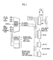
- a first embodiment of this invention is shown.
- the present invention proceeds by modifying existing on-chip hardware which includes, in a typical array forming a high speed RAM, a non-redundant memory with associated array/word decoders.
- the non-redundant portion is divided into eight groups of 16 words each.
- the word decoders (WD) are shown schematically as WD1-WD128.
- the TTL decoder input stage shown in Fig. 1 has seven emitters for address access to form the 128 word line array.
- the input stage of the decoder is shown in schematic form, it being understood that a conventional TTL decoder having seven emitters is modified in accordance with the present invention.
- the input stage of the decoder is used to access its associated memory cells, conventionally a bipolar circuits.
- the decoder applies "set”, “reset” signals to the base of transister Q, a bipolar device that switches select current to the memory cells. While a TTL decoder is shown, it is understood that a multi-level decoder or a current switch decoder may also be used. Such devices are well known in the art.
- the 128 non- redundant word decoders (WDI-WD128) are modified to have an extra emitter input. This extra emitter input is coupled to the output of a redundant address receiver compare circuit as shown in Fig. 1.
- the present invention also departs from conventional bipolar arrays by having a redundant portion disposed on-chip comprising 16 extra words WD129-WD144. Since the non-redundant portion is divided into eight groups of 16 words each, the additional 16 redundant words are equivalent to the addition of one additional word group.
- the 16 redundant word decoders WD129-WD144 require only 5 emitter inputs and the extra emitter inputs of those 16 redundant decoders are also coupled to the output of the redundant address receiver compare circuit. -
- Fig. 1 shows a first embodiment of the invention with the redundant receiver compare circuit receiving three word address inputs. These inputs are used for selecting the memory word group (one out of eight) to be accessed and are used by the compare circuit together with three redundant address inputs.
- the word address inputs are denoted in Fig. 1 as AO-A2 and the redundant address inputs are denoted as RAO-RA2.
- the three redundant address inputs are personalized on the module to correspond to a particular word group having one or more defective bits which are determined by initial testing of the chip.
- the defect may be either bad cells or word lines.
- the redundant receiver compare circuit provides an output as an up level true output and a down level complement output. This output causes the redundant word group WD129-WD144 to be selected in place of the known defective word group.
- the additional addresses then select one out of the 16 word lines in the redundant word group.
- the compare circuit has a disable input. With the disable input at a down level, the redundant address receiver will always replace one of the eight word groups by the redundant word group. Consequently, a defect in the redundant word group or its circuitry would cause the entire chip to be defective. This, however, will not impact the overall use, since with the disable input rendered active the compare circuit can be forced into the non-compare state, disabling the redundant word group and correspondingly enabling the other word groups. The chip can therefore be configured to function in the "all good" mode.
- the compare circuitry introduced to the chip can be implemented as a standard address-receiver decoder driver with compare logic input circuitry.
- the introduction of an extra emitter input to the TTL word decoders does not substantially impact chip space utilization.
- the bit circuitry itself is undisturbed by the redundancy introduced in accordance with the present invention.
- the implementation of the redundancy scheme shown in Fig. 1 has minimum impact on the chip in terms of density, chip function, power, performance, and input-output functions.
- the module itself is personalized either by the use of a permanent wire or by an engineering change wire during manufacture. Personalization can be made according to the defective word group.
- Fig. 2 does not include the decoder section, it being understood that the non-redundant section will comprise 128 words.
- the redundancy organization is different in the sense that the normal word lines are arranged as 16 groups of 8-words each as opposed to 8 groups of 16 words.
- a redundant word group therefore contains 8 additional word lines and decoders such that the redundant word group present requires less chip area.
- the redundant word group addresses are clocked into the shift register latches LO-L3 sequentially at the redundant address input synchronized with the clock input to each of the latches.
- the Fig. 2 embodiment allows the compare to be done on more addresses but still requires only two or three additional input-output lines for implementing redundancy. Accordingly, the Fig. 2 embodiment offers an organization having fewer redundant word lines in the redundant word group (8 as opposed to 16) and allows redundancy with less chip space required. This embodiment does not require the extra redundant address inputs of the Fig. 1 embodiment. However, as a design tradeoff the addresses of the failed word groups must be loaded into the latches at each system power-up.
- a word redundancy scheme for a high speed RAM is defined requiring minimal changes to the circuitry that have a minimal impact on chip performance.
- the introduction of an extra emitter for each of the word group decoders does not affect overall chip density and the introduction of compare circuit on-chip does not significantly influence chip power or I/O requirements.
- chip function and performance are maintained so that overall system throughput is not degraded.
Landscapes
- For Increasing The Reliability Of Semiconductor Memories (AREA)
- Static Random-Access Memory (AREA)
- Techniques For Improving Reliability Of Storages (AREA)
Applications Claiming Priority (2)
| Application Number | Priority Date | Filing Date | Title |
|---|---|---|---|
| US352916 | 1982-02-26 | ||
| US06/352,916 US4462091A (en) | 1982-02-26 | 1982-02-26 | Word group redundancy scheme |
Publications (3)
| Publication Number | Publication Date |
|---|---|
| EP0087610A2 true EP0087610A2 (de) | 1983-09-07 |
| EP0087610A3 EP0087610A3 (en) | 1987-02-04 |
| EP0087610B1 EP0087610B1 (de) | 1989-05-31 |
Family
ID=23387001
Family Applications (1)
| Application Number | Title | Priority Date | Filing Date |
|---|---|---|---|
| EP83101060A Expired EP0087610B1 (de) | 1982-02-26 | 1983-02-04 | Anordnung mit Direktzugriffsspeicher mit einem Wortredundanzschema |
Country Status (4)
| Country | Link |
|---|---|
| US (1) | US4462091A (de) |
| EP (1) | EP0087610B1 (de) |
| JP (1) | JPS58147900A (de) |
| DE (1) | DE3379986D1 (de) |
Cited By (9)
| Publication number | Priority date | Publication date | Assignee | Title |
|---|---|---|---|---|
| DE3405621A1 (de) * | 1983-02-17 | 1984-08-23 | Mitsubishi Denki K.K., Tokio/Tokyo | Halbleiter-speichereinrichtung |
| GB2154032A (en) * | 1984-02-08 | 1985-08-29 | Inmos Ltd | A repairable memory array |
| GB2165971A (en) * | 1984-10-19 | 1986-04-23 | Hitachi Ltd | A semiconductor memory |
| EP0178949A3 (en) * | 1984-10-19 | 1988-01-13 | Fujitsu Limited | Bipolar-transistor type semiconductor memory device having a redundancy configuration |
| EP0178948A3 (en) * | 1984-10-19 | 1988-01-13 | Fujitsu Limited | Bipolar-transistor random access memory having a redundancy configuration |
| EP0178950A3 (en) * | 1984-10-19 | 1988-02-24 | Fujitsu Limited | Bipolar-transistor type random access memory device having a redundancy configuration |
| EP0202892A3 (en) * | 1985-05-20 | 1988-09-07 | Fujitsu Limited | Semiconductor memory device with diode matrix decoder and redundancy configuration |
| EP0234907A3 (en) * | 1986-02-27 | 1989-04-26 | Fujitsu Limited | Semiconductor memory device with redundant memory cell |
| FR2647583A1 (fr) * | 1989-05-24 | 1990-11-30 | Samsung Electronics Co Ltd | Dispositif de memoire a semiconducteurs avec bloc redondant |
Families Citing this family (4)
| Publication number | Priority date | Publication date | Assignee | Title |
|---|---|---|---|---|
| US4599709A (en) * | 1984-02-17 | 1986-07-08 | At&T Bell Laboratories | Byte organized static memory |
| US6058052A (en) * | 1997-08-21 | 2000-05-02 | Cypress Semiconductor Corp. | Redundancy scheme providing improvements in redundant circuit access time and integrated circuit layout area |
| US6115300A (en) * | 1998-11-03 | 2000-09-05 | Silicon Access Technology, Inc. | Column redundancy based on column slices |
| US6724669B1 (en) * | 2002-05-08 | 2004-04-20 | Silicon Graphics, Inc. | System and method for repairing a memory column |
Family Cites Families (7)
| Publication number | Priority date | Publication date | Assignee | Title |
|---|---|---|---|---|
| US3753235A (en) * | 1971-08-18 | 1973-08-14 | Ibm | Monolithic memory module redundancy scheme using prewired substrates |
| JPS51128235A (en) * | 1975-04-30 | 1976-11-09 | Toshiba Corp | A semi-conductor integration circuit memory |
| JPS523764A (en) * | 1975-06-27 | 1977-01-12 | Hiroshi Shimizu | Filter apparatus for cattle excrement using chaff charcoals as filter aids for filtration |
| US4250570B1 (en) * | 1976-07-15 | 1996-01-02 | Intel Corp | Redundant memory circuit |
| JPS5384634A (en) * | 1976-12-30 | 1978-07-26 | Fujitsu Ltd | Ic memory unit device |
| JPS5928560Y2 (ja) * | 1979-11-13 | 1984-08-17 | 富士通株式会社 | 冗長ビットを有する記憶装置 |
| US4346459A (en) * | 1980-06-30 | 1982-08-24 | Inmos Corporation | Redundancy scheme for an MOS memory |
-
1982
- 1982-02-26 US US06/352,916 patent/US4462091A/en not_active Expired - Lifetime
- 1982-11-19 JP JP57202203A patent/JPS58147900A/ja active Granted
-
1983
- 1983-02-04 EP EP83101060A patent/EP0087610B1/de not_active Expired
- 1983-02-04 DE DE8383101060T patent/DE3379986D1/de not_active Expired
Cited By (10)
| Publication number | Priority date | Publication date | Assignee | Title |
|---|---|---|---|---|
| DE3405621A1 (de) * | 1983-02-17 | 1984-08-23 | Mitsubishi Denki K.K., Tokio/Tokyo | Halbleiter-speichereinrichtung |
| GB2154032A (en) * | 1984-02-08 | 1985-08-29 | Inmos Ltd | A repairable memory array |
| GB2165971A (en) * | 1984-10-19 | 1986-04-23 | Hitachi Ltd | A semiconductor memory |
| EP0178949A3 (en) * | 1984-10-19 | 1988-01-13 | Fujitsu Limited | Bipolar-transistor type semiconductor memory device having a redundancy configuration |
| EP0178948A3 (en) * | 1984-10-19 | 1988-01-13 | Fujitsu Limited | Bipolar-transistor random access memory having a redundancy configuration |
| EP0178950A3 (en) * | 1984-10-19 | 1988-02-24 | Fujitsu Limited | Bipolar-transistor type random access memory device having a redundancy configuration |
| EP0202892A3 (en) * | 1985-05-20 | 1988-09-07 | Fujitsu Limited | Semiconductor memory device with diode matrix decoder and redundancy configuration |
| EP0234907A3 (en) * | 1986-02-27 | 1989-04-26 | Fujitsu Limited | Semiconductor memory device with redundant memory cell |
| FR2647583A1 (fr) * | 1989-05-24 | 1990-11-30 | Samsung Electronics Co Ltd | Dispositif de memoire a semiconducteurs avec bloc redondant |
| NL9000227A (nl) * | 1989-05-24 | 1990-12-17 | Samsung Electronics Co Ltd | Halfgeleider-geheugeninrichting met redundant blok. |
Also Published As
| Publication number | Publication date |
|---|---|
| EP0087610A3 (en) | 1987-02-04 |
| US4462091A (en) | 1984-07-24 |
| JPS58147900A (ja) | 1983-09-02 |
| DE3379986D1 (en) | 1989-07-06 |
| JPS6237478B2 (de) | 1987-08-12 |
| EP0087610B1 (de) | 1989-05-31 |
Similar Documents
| Publication | Publication Date | Title |
|---|---|---|
| US5859804A (en) | Method and apparatus for real time two dimensional redundancy allocation | |
| US4281398A (en) | Block redundancy for memory array | |
| US5914907A (en) | Semiconductor memory device capable of increasing chip yields while maintaining rapid operation | |
| US4730320A (en) | Semiconductor memory device | |
| US3753244A (en) | Yield enhancement redundancy technique | |
| EP0096782B1 (de) | On-Line Neuausrichtung von Speicherfehlern | |
| US5493531A (en) | Integrated circuitry for checking the utilization rate of redundancy memory elements in a semiconductor memory device | |
| EP0689695B1 (de) | Fehlertolerantes speichersystem | |
| US5109360A (en) | Row/column address interchange for a fault-tolerant memory system | |
| JPH0322680B2 (de) | ||
| EP0087610B1 (de) | Anordnung mit Direktzugriffsspeicher mit einem Wortredundanzschema | |
| EP0090219B1 (de) | Speichersystem restruktuiert mittels deterministischem Permutationsalgorithmus | |
| US7231582B2 (en) | Method and system to encode and decode wide data words | |
| EP0096779B1 (de) | Mehrbit Fehlerstreuanordnung um einen fehlertoleranten Halbleiterspeicher zu beliefern | |
| US5025418A (en) | Semiconductor device for performing automatic replacement of defective cells | |
| JPS6237422B2 (de) | ||
| US6366508B1 (en) | Integrated circuit memory having column redundancy with no timing penalty | |
| US6507524B1 (en) | Integrated circuit memory having column redundancy | |
| EP0189699B1 (de) | Festwertspeicher mit interdigitalen Bitzeilen | |
| US5103424A (en) | Memory column interface with fault tolerance | |
| JPH0652697A (ja) | 誤り訂正機能付半導体メモリ | |
| US6076176A (en) | Encoding of failing bit addresses to facilitate multi-bit failure detect using a wired-OR scheme | |
| US7117428B2 (en) | Redundancy register architecture for soft-error tolerance and methods of making the same | |
| US6934202B2 (en) | Memory circuit with dynamic redundancy | |
| US7263011B2 (en) | Memory circuit with flexible bitline-related and/or wordline-related defect memory cell substitution |
Legal Events
| Date | Code | Title | Description |
|---|---|---|---|
| PUAI | Public reference made under article 153(3) epc to a published international application that has entered the european phase |
Free format text: ORIGINAL CODE: 0009012 |
|
| AK | Designated contracting states |
Designated state(s): DE FR GB |
|
| 17P | Request for examination filed |
Effective date: 19831215 |
|
| PUAL | Search report despatched |
Free format text: ORIGINAL CODE: 0009013 |
|
| AK | Designated contracting states |
Kind code of ref document: A3 Designated state(s): DE FR GB |
|
| 17Q | First examination report despatched |
Effective date: 19871109 |
|
| GRAA | (expected) grant |
Free format text: ORIGINAL CODE: 0009210 |
|
| AK | Designated contracting states |
Kind code of ref document: B1 Designated state(s): DE FR GB |
|
| REF | Corresponds to: |
Ref document number: 3379986 Country of ref document: DE Date of ref document: 19890706 |
|
| ET | Fr: translation filed | ||
| PLBE | No opposition filed within time limit |
Free format text: ORIGINAL CODE: 0009261 |
|
| STAA | Information on the status of an ep patent application or granted ep patent |
Free format text: STATUS: NO OPPOSITION FILED WITHIN TIME LIMIT |
|
| 26N | No opposition filed | ||
| PGFP | Annual fee paid to national office [announced via postgrant information from national office to epo] |
Ref country code: GB Payment date: 19930118 Year of fee payment: 11 |
|
| PGFP | Annual fee paid to national office [announced via postgrant information from national office to epo] |
Ref country code: FR Payment date: 19930120 Year of fee payment: 11 |
|
| PGFP | Annual fee paid to national office [announced via postgrant information from national office to epo] |
Ref country code: DE Payment date: 19930127 Year of fee payment: 11 |
|
| PG25 | Lapsed in a contracting state [announced via postgrant information from national office to epo] |
Ref country code: GB Effective date: 19940204 |
|
| GBPC | Gb: european patent ceased through non-payment of renewal fee |
Effective date: 19940204 |
|
| PG25 | Lapsed in a contracting state [announced via postgrant information from national office to epo] |
Ref country code: FR Effective date: 19941031 |
|
| PG25 | Lapsed in a contracting state [announced via postgrant information from national office to epo] |
Ref country code: DE Effective date: 19941101 |
|
| REG | Reference to a national code |
Ref country code: FR Ref legal event code: ST |