EP0088312A2 - Circuit de commutation en forme de H avec un circuit de protection contre les courants excessifs - Google Patents
Circuit de commutation en forme de H avec un circuit de protection contre les courants excessifs Download PDFInfo
- Publication number
- EP0088312A2 EP0088312A2 EP83101881A EP83101881A EP0088312A2 EP 0088312 A2 EP0088312 A2 EP 0088312A2 EP 83101881 A EP83101881 A EP 83101881A EP 83101881 A EP83101881 A EP 83101881A EP 0088312 A2 EP0088312 A2 EP 0088312A2
- Authority
- EP
- European Patent Office
- Prior art keywords
- base
- transistor
- emitter
- collector
- power source
- Prior art date
- Legal status (The legal status is an assumption and is not a legal conclusion. Google has not performed a legal analysis and makes no representation as to the accuracy of the status listed.)
- Granted
Links
Images

Classifications
-
- H—ELECTRICITY
- H03—ELECTRONIC CIRCUITRY
- H03K—PULSE TECHNIQUE
- H03K17/00—Electronic switching or gating, i.e. not by contact-making and –breaking
- H03K17/08—Modifications for protecting switching circuit against overcurrent or overvoltage
- H03K17/082—Modifications for protecting switching circuit against overcurrent or overvoltage by feedback from the output to the control circuit
- H03K17/0826—Modifications for protecting switching circuit against overcurrent or overvoltage by feedback from the output to the control circuit in bipolar transistor switches
-
- H—ELECTRICITY
- H02—GENERATION; CONVERSION OR DISTRIBUTION OF ELECTRIC POWER
- H02P—CONTROL OR REGULATION OF ELECTRIC MOTORS, ELECTRIC GENERATORS OR DYNAMO-ELECTRIC CONVERTERS; CONTROLLING TRANSFORMERS, REACTORS OR CHOKE COILS
- H02P7/00—Arrangements for regulating or controlling the speed or torque of electric DC motors
- H02P7/03—Arrangements for regulating or controlling the speed or torque of electric DC motors for controlling the direction of rotation of DC motors
- H02P7/04—Arrangements for regulating or controlling the speed or torque of electric DC motors for controlling the direction of rotation of DC motors by means of a H-bridge circuit
Definitions
- This invention relates to an H-switch circuit in use, for example, for driving a DC motor in a forward or reverse direction.
- H-switch for controlling the rotation of a DC motor is disclosed in Japanese Patent Disclosure (KOKAI) No. 56-66932, for example.
- the H-switch is comprised of two pairs of transistors with the emitter-collector paths connected in series between two power sources. Nodes between the emitter-collector paths of the paired transistors are used as output terminals of the switch circuit.
- the rotating direction of the DC motor is controlled according to the signals applied to the bases of the two pairs of transistors.
- an object of the present invention is to provide an H-switch circuit with an overcurrent protection circuit which can protect all the output transistors from an overcurrent and has a relatively simple circuit arrangement.
- the H-switch circuit comprises overcurrent-detecting circuits, which are respectively provided for output transistors in order to detect an output transistor having an overcurrent, a circuit for logically summing the output signals from the overcurrent-detecting circuits, an integrating circuit controlled to be in a charge or discharge state according to the output signal from said logical summing circuit, and a circuit for turning off the output transistors when said integrating circuit is in the charge state and setting the integrating circuit to a discharge state.
- the charge and discharge operations of the integrating circuit are intermittently repeated until the overcurrent of the output transistor is reduced to zero.
- the output transistors may be protected from the overcurrent.
- the overcurrent-protection period is much longer than the overcurrent-detecting period. This indicates that the heat generated from the switch circuit is small. Further, the output transistors are turned off while at the same time the operating state of the integrating circuit is automatically inverted. This feature implies that there is no need for a separate operation to restore the normal operation of the circuit.
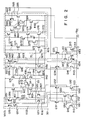
- V ccl' V cc2 and V EE are power sources.
- Ql to Q4 are output transistors.
- Overcurrent-detecting resistor pairs Rll, R12), (R21, R22), (R31, R32) and (R41, R42) are respectively connected across the base-emitter paths of these output transistors, as shown.
- the transistors Q2 and Q2' and Q4 and Q4' are connected in a Darlington fashion.
- a collector output of a second transistor Q12 is applied to the base of the transistor Q2' to drive it.
- the transistor Q12 is connected at the base to a second voltage input terminal 2, by way of a resistor R23.
- the emitter of the transistor Q12 is connected to the power source V EE (ground terminal).
- the collector of the same is connected to the power source V ccl' through a transistor Q32 for a bias current source.
- a first input transistor Qll is connected at the base through a base resistor R13 to a first voltage input terminal 1. The same transistor is grounded at the emitter, and at the collector to the power source V cc1 ' via a transistor for a bias current source.
- the collector output of the first input transistor Qll is applied to the base of the output transistor Ql, through a Ql drive circuit 50 composed of transistors (Q51, Q52, Q53) and (Q54, Q55, Q56) each forming a current mirror circuit, and resistors R51, R52 and R53.
- a third input transistor Q13 is connected at the base through a resistor R33 to a third voltage input terminal 3.
- the same resistor is connected at the emitter to ground and at the collector to the power source V ccl' via a transistor Q33 for a bias current source.
- the collector output of the third input transistor Q13 is applied to the base of the output transistor Q3, through a Q3 drive circuit 60 composed of transistors (Q61, Q62, Q63) and (Q64, Q65, Q66) each forming a current mirror circuit, and resistors R61, R62 and R63.
- a fourth input transistor Q14 is connected at the base through a resistor R43 to a fourth voltage input terminal 4. The same resistor is connected at the emitter to ground and at the collector to the power source Vccl, via a transistor Q34 for a bias current source. The collector output of the fourth input transistor Q14 is applied as a drive input to the base of the transistor Q4'.
- the base-emitter path of a transistor Q15 is connected across the resistor Rll, and the collector of the transistor Q15 is grounded through the resistors R15 and R16 in this order.
- a first detecting transistor Q21 is connected at the base to a node between the resistors R15 and R16. The same transistor is connected at the emitter to ground and at the collector to an overcurrent detecting line 20.
- the base-emitter path of a transistor Q16 is connected across the resistor R31 and the collector of the transistor is grounded through the resistors R35 and R36 in this order.
- a third detecting transistor Q23 is connected at the base to a node between the resistors R35 and R36. The same transistor is connected at the emitter to ground and at the collector to the overcurrent detecting line 20.
- the second detecting transistor Q22 is connected at the base to a node between resistors R21 and R22, at the emitter to ground and at the collector to the overcurrent detecting line 20.
- a fourth detecting transistor Q24 is connected at the base to a node between resistors R41 and R42, at the emitter to ground and at the collector to the overcurrent detecting line 20.
- a transistor Q71 is connected at the base to the overcurrent detecting line 20 and to the power source V ccl via a resistor R71.
- the collector of the same transistor is connected to the base of a transistor Q72 and to the collector of a transistor Q73 for a current source.
- the transistor Q72 is connected at the collector to the power source V cc1 .
- the emitter of the same transistor is connected to the base of a transistor Q74 and to the collector of a transistor Q75 and to ground by the way of a capacitor C.
- the emitter and the base of the transistor Q75 are grounded together, and the emitter of the transistor Q74 is connected to the collector of a transistor Q76 for a current source.
- the transistor Q76 for the current source is connected at the emitter to ground through a resistor R72, and is connected at the base to a bias power source V B1 of 0.7 V, for example, together with the base of the transistor Q73 for the current source.
- the emitter of the transistor Q73 is grounded through a resistor R73.
- the collector of the transistor Q74 is connected to the collector of the transistor Q77 of which the emitter and base are connected to the power source V cc1.
- the base of the transistor Q81 is connected to the collector of the transistor Q77.
- a transistor Q82 is provided so as to form an equivalent pnp transistor together with the transistor Q81.
- the transistor Q81 is connected at the emitter to the power source V cc1 , and at the collector to the base of the transistor Q82.
- the transistor Q82 is connected at the collector to the power source V cc1 , and has a resistor 81 between the base and emitter.
- the emitter of the transistor Q82 is connected to the emitter of the transistor Q82 and the collector of the transistor Q84.
- the base of the current source transistor Q84 is connected to the bias source V B2 of 1.2 V, for example, and its emitter is grounded by way of a resistor R82.
- the transistor Q83 has its base and collector connected together, and further connected to the base of the transistor Q85 and the collector of the transistor Q86.
- the transistor Q86 is connected at the emitter to the power source V cc1 via a resistor R83, and at the base to the node between resistors R84 and R85.
- the other end of the resistor R84 is connected to the power source V cc1 and the other end of the resistor R85 is connected to the emitter of the transistor Q85.
- the collector of the transistor Q85 is grounded.
- a node between the resistors R84 and R85 is connected to the bases of the transistors Q31 to Q34 as bias current sources.
- the power source V cc1 is used for the logic circuit and the power source V cc2 for the output transistors. These are equivalent to the V cc in Fig. 1, and V cc2 is larger than Vccl.
- the H switch with an overcurrent-protection circuit is fabricated into an integrated circuit.
- the load 13 is connected between the output terminals 11 and 12.
- the second input transistor Q12 is turned on and the output transistors Q2' and Q2 are turned off.
- the third transistor Q13 is turned on and the transistor Q66 of the Q3 drive circuit 60 is turned off, so that the output transistor Q3 is turned off.
- the output transistors Ql and Q4 are turned off but the transistors Q2 and Q3 are turned on, through a process similar to the above. Accordingly, current flows from the transistor Q3 to the transistor Q2 through the load circuit 13.
- the base-emitter voltage V BE of this transistor is about 1 V (in the case of the integrated transistor) and is larger than the base-emitter voltage V BE (about 0.7 V) of a transistor through which the short current does not flow. Accordingly, any one of the resistors (Rll, R12), (R21, R22), (R31, R32) and (R41, R42) may detect the large voltage V BE' and any of the transistors (Q15, Q21), Q22, (Q16, Q23) and Q24 may be turned on. In the integrating circuit 70, the transistor Q71 and the transistor Q72 are turned on in succession.
- the capacitor C is rapidly charged, so that the base voltage of the transistor Q74 rapidly rises to the voltage of the power source V cc1 , as. illustrated in Fig. 3.
- the transistor Q74 is driven by the transistor Q72 and turned on.
- the transistors Q81 and Q82 are turned on, while the transistors Q85 and Q86 are turned off.
- the output voltage at the node between the resistors R84 and R85 rises. Therefore, the transistors Q31 to Q34 are in an ON state.
- the output transistors Ql to Q4 are left OFF, that is, these transistors are in an overcurrent-prohibiting condition.
- the overcurrent-detecting transistors Q21 to Q24 are turned off, as are the transistors Q71 and Q72 in the integrating circuit 70. Then, the charge stored in the capacitor C is gradually discharged therefrom as the base current of the transistor Q74. If the current of the transistor Q76 is about 10 ⁇ A and the common emitter current amplification factor S of the transistor Q74 is about 100, the base current I B is about 0.1 ⁇ A.
- the transistor Q74 During the time that the base voltage of the transistor Q74 slowly drops, as above, the transistor Q74 remains in the ON state. As previously stated, the output voltage of the current source circuit 80 is raised. The output transistors Ql to Q4 are in an overcurrent-prohibiting condition.
- the transistors Q81 and Q82 are then turned off and the transistors Q85 and Q86 are in an active 'state in the current source circuit 80.
- the result is that the output voltage drops to a predetermined value and the current source transistors Q31 to Q34 are in an active state.
- the H-switch circuit is restored to its normal state and is ready for detecting another overcurrent problem.
- the overcurrent-detecting operation will be repeated intermittently.
- the overcurrent-prohibiting period (discharge period of the capacitor C) is sufficiently longer than the overcurrent-detecting period (charge period of the capacitor C) T'. Because of this feature, the output transistors Ql to Q4 are prevented from being damaged, and a lesser amount of power is consumed, resulting in negligible heating of the integrated circuit.
- the shorted transistor has a peak current Ip of 1 A
- the charge period T' of the integrated capacitor is 10 ⁇ s
- the discharge period T is 1 ms.
- An average current Ia in this case, is
- the output transistors Ql to Q4 at least have to be set in an OFF state according to the operating state of the integrating circuit 70.
- the effect attained by turning off the overcurrent-detecting transistors Q21 to Q24 according to the operating state of the integrating circuit 70 may of course be attained by inverting the operating state of the integrating circuit 70.
- the base-emitter voltages of the output transistors are respectively detected by the corresponding overcurrent-detecting transistors.
- the outputs of the overcurrent-detecting transistors are logically summed.
- the logical sum obtained is then used to control the charge/discharge operation of the integrating circuit.
- the integrating circuit produces a control signal according to the charge/discharge operating state. With this control signal, the output transistors are turned off and at the same time the operating state of the integrating circuit is inverted.
- the H-switch thus arranged allows an overcurrent-detecting operation to be intermittently performed.
- the H-switch may be realized by a relatively simple circuit arrangement.
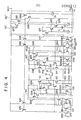
- FIG. 4 another embodiment of the invention is shown.
- the circuit arrangement of this second embodiment is basically the same as that of the first embodiment, although some portions of the circuit are more simplified.
- the same portions as those in Fig. 2 are designated by the same symbols and the equivalent portions by the same symbols primed.
- reference number 50' designates a Ql drive circuit; 60' a Q3 drive circuit; 70' an integrating circuit; and 80' a bias current source circuit.
- Il and I2 represent bias current source circuits.
- I3 is a bias current source.
Landscapes
- Engineering & Computer Science (AREA)
- Power Engineering (AREA)
- Electronic Switches (AREA)
- Emergency Protection Circuit Devices (AREA)
- Protection Of Generators And Motors (AREA)
- Protection Of Static Devices (AREA)
Applications Claiming Priority (2)
| Application Number | Priority Date | Filing Date | Title |
|---|---|---|---|
| JP34463/82 | 1982-03-04 | ||
| JP57034463A JPS58151814A (ja) | 1982-03-04 | 1982-03-04 | 過電流保護回路付きhスイツチ回路 |
Publications (3)
| Publication Number | Publication Date |
|---|---|
| EP0088312A2 true EP0088312A2 (fr) | 1983-09-14 |
| EP0088312A3 EP0088312A3 (en) | 1985-01-09 |
| EP0088312B1 EP0088312B1 (fr) | 1988-04-20 |
Family
ID=12414938
Family Applications (1)
| Application Number | Title | Priority Date | Filing Date |
|---|---|---|---|
| EP83101881A Expired EP0088312B1 (fr) | 1982-03-04 | 1983-02-25 | Circuit de commutation en forme de H avec un circuit de protection contre les courants excessifs |
Country Status (4)
| Country | Link |
|---|---|
| US (1) | US4633358A (fr) |
| EP (1) | EP0088312B1 (fr) |
| JP (1) | JPS58151814A (fr) |
| DE (1) | DE3376374D1 (fr) |
Cited By (3)
| Publication number | Priority date | Publication date | Assignee | Title |
|---|---|---|---|---|
| EP0374490A3 (fr) * | 1988-12-21 | 1990-08-08 | STMicroelectronics S.r.l. | Circuit comparateur de tension pour circuits intégrés d'attaque de charges inductives |
| EP0415439A3 (en) * | 1989-09-01 | 1992-03-04 | Kabushiki Kaisha Toshiba | Composite semiconductor device having function for overcurrent detection |
| WO2009086445A1 (fr) * | 2007-12-28 | 2009-07-09 | Eaton Corporation | Circuit d'attaque et son procédé d'utilisation |
Families Citing this family (23)
| Publication number | Priority date | Publication date | Assignee | Title |
|---|---|---|---|---|
| JPS6248123U (fr) * | 1985-09-09 | 1987-03-25 | ||
| JP2573946B2 (ja) * | 1987-04-20 | 1997-01-22 | 富士通株式会社 | 半導体集積回路 |
| US5040088A (en) * | 1987-10-05 | 1991-08-13 | Chloride Group Public Limited Company | Electric motor controllers |
| USRE34159E (en) * | 1987-10-05 | 1993-01-12 | Chloride Group Public Limited Co. | Electric motor controllers |
| KR930011196B1 (ko) * | 1988-11-16 | 1993-11-25 | 롬 가부시끼가이샤 | 모터 구동회로 |
| JPH0288491U (fr) * | 1988-12-20 | 1990-07-12 | ||
| JP2564094Y2 (ja) * | 1989-03-31 | 1998-03-04 | 沖電気工業株式会社 | プリンタ |
| US5192901A (en) * | 1990-03-16 | 1993-03-09 | Cherry Semiconductor Corporation | Short circuit protection |
| US5117167A (en) * | 1990-11-01 | 1992-05-26 | Rotron, Incorporated | Commutating energy suppression circuit for an electronically commutated DC motor |
| US5103148A (en) * | 1990-11-06 | 1992-04-07 | Motorola, Inc. | Low voltage circuit to control high voltage transistor |
| JPH04327953A (ja) * | 1991-04-30 | 1992-11-17 | Oki Electric Ind Co Ltd | アラーム制御方法 |
| IT1251205B (it) * | 1991-09-18 | 1995-05-04 | St Microelectronics Srl | Circuito a ponte ad h con protezione contro la conduzione incrociata durante l'inversione della corrente nel carico. |
| JP3252045B2 (ja) * | 1993-12-24 | 2002-01-28 | 株式会社ゼクセルヴァレオクライメートコントロール | パルスモータ制御装置 |
| US5751171A (en) * | 1995-03-22 | 1998-05-12 | Vtc Inc. | Predriver for fast current switching through a two-terminal inductive load |
| US5781046A (en) * | 1995-03-22 | 1998-07-14 | Vtc, Inc. | Push-and-pull driver circuit for driving an H-bridge coupled to a two-terminal inductive load |
| US5773991A (en) * | 1995-05-02 | 1998-06-30 | Texas Instruments Incorporated | Motor current sense circuit using H bridge circuits |
| US5859519A (en) * | 1997-05-29 | 1999-01-12 | General Electric Company | Single phase motor drive |
| US5977734A (en) * | 1998-09-09 | 1999-11-02 | Stmicroelectronics, Inc. | Circuit and method for determining optimal phase combination for startup of a polyphase DC motor |
| SG100645A1 (en) * | 2000-03-31 | 2003-12-26 | Inventio Ag | Auxiliary device for displacing a payload receptacle of a lift and device for monitoring the position and the movement of a cage in a shaft of a lift |
| JP3858219B2 (ja) * | 2001-10-25 | 2006-12-13 | ミネベア株式会社 | ブラシレス直流1相モータのプリドライブ回路 |
| CN100561848C (zh) * | 2004-03-12 | 2009-11-18 | Mks仪器股份有限公司 | 用于开关式电源的控制电路 |
| US7116110B1 (en) | 2005-06-30 | 2006-10-03 | Yazaki North America, Inc. | Sensorless protection for electronic device |
| JP4774427B2 (ja) * | 2008-06-30 | 2011-09-14 | 株式会社日立製作所 | エレベータの位置検出装置、並びにエレベータ |
Family Cites Families (13)
| Publication number | Priority date | Publication date | Assignee | Title |
|---|---|---|---|---|
| DE1413923A1 (de) * | 1961-04-12 | 1968-11-28 | Licentia Gmbh | Schutzeinrichtung fuer Schalttransistoreinrichtungen |
| US3332007A (en) * | 1964-08-20 | 1967-07-18 | Ling Temco Vought Inc | Motor control circuit with time delay |
| DE2059884A1 (de) * | 1970-12-05 | 1972-06-15 | Siemens Ag | Kollektorloser Gleichstrommotor mit einem Dauermagnetlaeufer und einer aus mehreren Teilwicklungen bestehenden Staenderwicklung |
| FR2180144A5 (fr) * | 1972-04-10 | 1973-11-23 | Honeywell Bull | |
| DE2361645B2 (de) * | 1972-12-12 | 1976-10-28 | Pioneer Electronic Corp., Tokio | Elektronische ueberstromschutzschaltungsanordnung |
| US3919600A (en) * | 1973-03-19 | 1975-11-11 | Detprotector Inc | Overload current protector for A. C. motors |
| JPS576806B2 (fr) * | 1973-10-05 | 1982-02-06 | ||
| US4006370A (en) * | 1975-12-15 | 1977-02-01 | General Electric Company | Fast turn-off circuit for power transistor |
| JPS5666932A (en) * | 1979-11-06 | 1981-06-05 | Rohm Co Ltd | Absorption circuit of counter electromotive force for direct current load drive circuit |
| US4322770A (en) * | 1980-02-28 | 1982-03-30 | Rca Corporation | Latch-up prevention circuit for power output devices using inductive loads |
| US4336562A (en) * | 1981-02-23 | 1982-06-22 | General Motors Corporation | H-Switch having short to plus protection |
| US4410935A (en) * | 1981-03-23 | 1983-10-18 | General Signal Corporation | Current overload protection for inverter of uninterruptible power supply system |
| US4532567A (en) * | 1983-02-18 | 1985-07-30 | General Motors Corporation | Electric power steering stall protection circuit |
-
1982
- 1982-03-04 JP JP57034463A patent/JPS58151814A/ja active Granted
-
1983
- 1983-02-25 DE DE8383101881T patent/DE3376374D1/de not_active Expired
- 1983-02-25 EP EP83101881A patent/EP0088312B1/fr not_active Expired
-
1985
- 1985-02-19 US US06/703,445 patent/US4633358A/en not_active Expired - Lifetime
Cited By (4)
| Publication number | Priority date | Publication date | Assignee | Title |
|---|---|---|---|---|
| EP0374490A3 (fr) * | 1988-12-21 | 1990-08-08 | STMicroelectronics S.r.l. | Circuit comparateur de tension pour circuits intégrés d'attaque de charges inductives |
| EP0415439A3 (en) * | 1989-09-01 | 1992-03-04 | Kabushiki Kaisha Toshiba | Composite semiconductor device having function for overcurrent detection |
| WO2009086445A1 (fr) * | 2007-12-28 | 2009-07-09 | Eaton Corporation | Circuit d'attaque et son procédé d'utilisation |
| US9998108B2 (en) | 2007-12-28 | 2018-06-12 | Eaton Intelligent Power Limited | Drive circuit and method of using the same |
Also Published As
| Publication number | Publication date |
|---|---|
| EP0088312B1 (fr) | 1988-04-20 |
| DE3376374D1 (en) | 1988-05-26 |
| EP0088312A3 (en) | 1985-01-09 |
| US4633358A (en) | 1986-12-30 |
| JPS58151814A (ja) | 1983-09-09 |
| JPH0145806B2 (fr) | 1989-10-04 |
Similar Documents
| Publication | Publication Date | Title |
|---|---|---|
| EP0088312B1 (fr) | Circuit de commutation en forme de H avec un circuit de protection contre les courants excessifs | |
| US4791314A (en) | Oscillation-free, short-circuit protection circuit | |
| GB2090489A (en) | Overcurrent protection apparatus for dc motors | |
| EP0267853B1 (fr) | Circuit d'attaque du type "bootstrap" à haute vitesse de commutation | |
| EP0268531B1 (fr) | Circuit pour la commutation à transistors bipolaires | |
| JP3675371B2 (ja) | 電圧レギュレータ | |
| CA1055574A (fr) | Circuit logique d'attaque avec protection de sortie | |
| US5148092A (en) | Stepping motor driving circuit having failsafe function | |
| US3934157A (en) | TTL circuit | |
| US4242605A (en) | Transient array drive for bipolar ROM/PROM | |
| US7215093B2 (en) | Motor drive circuit and motor drive method that can positively perform a brake operation | |
| JPH0473327B2 (fr) | ||
| JP3710616B2 (ja) | トランジスタ保護回路および出力電力増幅回路 | |
| JP3945340B2 (ja) | 演算増幅器 | |
| JPS6053488B2 (ja) | ゲ−トタ−ンオフサイリスタのゲ−ト回路 | |
| KR100354726B1 (ko) | 집적형 전력 증폭단을 제어하기 위한 방법 및 장치 | |
| CN221079622U (zh) | 一种硬盘驱动模块 | |
| US20260012001A1 (en) | Electronic Fuse Driver Interface | |
| US4458286A (en) | Electronic device having a high voltage breakdown protection circuit | |
| JP3214225B2 (ja) | 多電源型比較回路 | |
| JPS6247367B2 (fr) | ||
| KR0116901Y1 (ko) | 카 로직 데크의 과전압 방지회로 | |
| CN117373495A (zh) | 硬盘驱动模块及对应的车载设备一体机 | |
| KR930007840Y1 (ko) | 3상태 출력 버퍼 회로 | |
| JPS6129574B2 (fr) |
Legal Events
| Date | Code | Title | Description |
|---|---|---|---|
| PUAI | Public reference made under article 153(3) epc to a published international application that has entered the european phase |
Free format text: ORIGINAL CODE: 0009012 |
|
| 17P | Request for examination filed |
Effective date: 19830322 |
|
| AK | Designated contracting states |
Designated state(s): DE FR GB IT |
|
| RAP1 | Party data changed (applicant data changed or rights of an application transferred) |
Owner name: KABUSHIKI KAISHA TOSHIBA |
|
| PUAL | Search report despatched |
Free format text: ORIGINAL CODE: 0009013 |
|
| AK | Designated contracting states |
Designated state(s): DE FR GB IT |
|
| 17Q | First examination report despatched |
Effective date: 19860317 |
|
| R17C | First examination report despatched (corrected) |
Effective date: 19860811 |
|
| GRAA | (expected) grant |
Free format text: ORIGINAL CODE: 0009210 |
|
| AK | Designated contracting states |
Kind code of ref document: B1 Designated state(s): DE FR GB IT |
|
| ITF | It: translation for a ep patent filed | ||
| REF | Corresponds to: |
Ref document number: 3376374 Country of ref document: DE Date of ref document: 19880526 |
|
| ET | Fr: translation filed | ||
| PLBE | No opposition filed within time limit |
Free format text: ORIGINAL CODE: 0009261 |
|
| STAA | Information on the status of an ep patent application or granted ep patent |
Free format text: STATUS: NO OPPOSITION FILED WITHIN TIME LIMIT |
|
| 26N | No opposition filed | ||
| ITTA | It: last paid annual fee | ||
| PGFP | Annual fee paid to national office [announced via postgrant information from national office to epo] |
Ref country code: FR Payment date: 19970211 Year of fee payment: 15 |
|
| PGFP | Annual fee paid to national office [announced via postgrant information from national office to epo] |
Ref country code: GB Payment date: 19970217 Year of fee payment: 15 |
|
| PGFP | Annual fee paid to national office [announced via postgrant information from national office to epo] |
Ref country code: DE Payment date: 19970228 Year of fee payment: 15 |
|
| PG25 | Lapsed in a contracting state [announced via postgrant information from national office to epo] |
Ref country code: GB Free format text: LAPSE BECAUSE OF NON-PAYMENT OF DUE FEES Effective date: 19980225 |
|
| PG25 | Lapsed in a contracting state [announced via postgrant information from national office to epo] |
Ref country code: FR Free format text: THE PATENT HAS BEEN ANNULLED BY A DECISION OF A NATIONAL AUTHORITY Effective date: 19980228 |
|
| GBPC | Gb: european patent ceased through non-payment of renewal fee |
Effective date: 19980225 |
|
| PG25 | Lapsed in a contracting state [announced via postgrant information from national office to epo] |
Ref country code: DE Free format text: LAPSE BECAUSE OF NON-PAYMENT OF DUE FEES Effective date: 19981103 |
|
| REG | Reference to a national code |
Ref country code: FR Ref legal event code: ST |